Note: Descriptions are shown in the official language in which they were submitted.
CA 02226512 2005-05-04
The invention relates to a ballast circuit for operating a lamp.
GB 2151115A discloses a ballast circuit in which control means inhibit or
enable the operation of the ballast circuit in response to an :interruption of
the mains
supply voltage. Switching lamps on and off by interrupting the mains supply
voltage
is also called the "toggle method". A disadvantage of the known ballast
circuit is that
when several lamps are operated in parallel by means of the same ballast
circuit, all
these lamps are either on or off and it is impossible to operate only some of
the lamps.
The invention aims to overcome this disadvantage and provide a more versatile
ballast circuit.
A ballast circuit according to the invention includes ballast means for
generating a high frequency lamp current from a mains power supply and
delivering
the lamp current to said lamp; and
control means connected between the ballast means and the lamp and adapted
to control power supplied to the lamp by the ballast means in response to
interruption
of the mains power supply;
wherein the ballast means is adapted to operate a plurality of lamps in
parallel
and the control means includes a switching element in series arrangement with
only
some of the lamps during lamp operation, and a control circuit for operating
the
CA 02226512 2005-05-04
2
t
If for instance only one ballast circuit is used to operate all the lamps in a
room, it
is possible to switch part of these lamps on and off using the main switch.
Important
advantages of the invention are thus that one wall switch can .control
multiple ballasts
and/or multiple lamps and no extra wire or extra switches are required in the
installation
of ballast circuits according to the invention. Thus the invention provides a
low cost
solution for light intensity control.
Good results have been obtained for ballast circuits according to the
invention wherein the switching element is a triac. Preferably the control
circuit comprises a
flipflop, a transistor (preferably a metal oxide field effect transistor), and
a Schmitt trigger.
Preferably the control circuit changes the conductive state of the switching
element only when the interruption of the mains supply voltage is shorter than
a
predetermined time interval. When the predetermined time interval is long
enough, e.g. 5
seconds the toggling may be performed quickly or leisurely, so long as the
entire toggle
cycle is completed within a predetermined amount of time. Preferably also; the
control.
circuit comprises reset means for rendering the switching element conductive
when the
interruption of the mains voltage is longer than said predetermined time
interval. When the
lamps are first switched on after having been extinguished for longer than
said predetermined
time interval, all the lamps are lit.
The invention will be further explained rnaking use of a drawing.
In the drawing:
FIG. 1 shows a block diagram of a Lighting system which includes an
exemplary embodiment of the invention;
FIG 2 shows an exemplary embodiment of the invention for a four lamp
instant start electronic ballast;
FIGS, 3,4, and 5 show how to employ a flip-flop to construct a Schmitt
trigger, in accordance with an aspect of the invention; and
FIG. 6 shows a modified version of the FIG. 2 embodiment of the
invention which may be used to insure that a 50% input power reduction will
result when
half of the lamps are off.
CA 02226512 1998-O1-07
WO 97/43880 3 PCTlIB97/00467
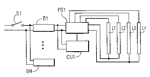
FIG. I shows a block diagram of a lighting system which includes an
exemplary embodiment of the invention. As shown, wall switch S 1 controls
multiple ballasts
B1...BN. In accordance with the principles of the invention, the output of
ballast B1 is
coupled as an input to each of power switch PS 1 and control unit CU 1.
Control unit CU 1
determines how many of lamps L1...L4 should be lit as a function of the
operation of wall
switch S 1. Power switch PS I causes the number of lamps determined by control
unit CU 1 to
be lit in response to commands from control unit CU1 and the presence or
absence of lamp
drive power at the output of ballast B1. Each ballast and lamp set may be
independently
controlled by their own control unit and power switch (not shown). In
accordance with an
IO aspect of the invention, each control unit and power switch may control
which of their lamps
are lit independent of any other control units or power switch units, even
ones that are
connected to the same wall switch.
FIG 2 shows an exemplary embodiment of the invention for a four lamp
instant start electronic ballast. In this embodiment, lamps L1 and L2 are
driven by ballast
output transformer T21 of ballast B 1 via capacitors C 1 OA and C 1 OB. Thus,
the lighting
state of lamps Ll and L2 corresponds directly to the output presence of lamp
drive power at
the of ballast output transformer T21. However, in accordance with an aspect
of the
invention, the lighting of lamps L3 and L4 is controlled by triac TH101 in
conjunction with
the output of ballast transformer T21. When triac TH 101 is on in the presence
of an output
voltage supplied by ballast output transformer T21, lamps L3 and L4 are lit.
Otherwise,
lamps L3 and L4 are off. Note that ballast output transformer T21 has two
secondary
windings.
In more detail, diode D 103 and capacitor C 104 provide a direct current
(DC) voltage for driving triac TH101. Resistor 8105 limits the triac drive
current. Metal
oxide semiconductor field effect transistor {MOSFET) QI01 controls the trigger
input of triac
THI01. When the gate of MOSFET Q101 has a high voltage supplied as an input
thereto,
MOSFET Q101 turns on. This, in turn, causes triac TH101 to be turned on as
well, resulting
in ignition of lamps L3 and L4. When the voltage supply to the gate of MOSFET
Q101 is
zero, MOSFET Q101 is off, as are triac TH101 and lamps L3 and L4. Thus, the
voltage
' 30 level at the gate of MOSFET Q101 controls the lighting of lamps L3 and
L4.
MOSFET Q101 is driven, for example, by flip-flop IC1-B, which is half
. of dual D flip-flop IC 1. A dual D flip-flop suitable for use as IC 1 is the
MC 140I3. Diode
D 102 and capacitor C 102 provide a DC power supply for dual D flip-flop IC 1.
Capacitor
C103 and resistor 8104 provide a narrow pulse which sets flip-flop IC1-B's Q
output to high
CA 02226512 1998-O1-07
WO 97/43880 4 PCT/IB97/00467
when the DC power supply is camping up. Since the Q output of flip-flop IC1-B
controls
MOSFET Q101, and hence triac THI01, all 4 lamps v'vrill turn on when the main
power turns
on and prior thereto there was insufficient DC power to operate IC1.
Advantageously, to drive a MOSFET requires almost no current.
Likewise, an MC 14013 dual D flip-flop chip, since it is a CMOS integrated
circuit,
consumes very little current. Thus, the power supply far ICI can sustain
itself for a certain
amount of time, which mainly is a function of the values of capacitor C 102
and resistor
8103. The values of capacitor C I02 and resistor 8103 are selected, for
example, such that
sufficient DC power is supplied to operate ICI for approximately 5 seconds
after the ballast
input power is turned off. This means that IC1 can perform its normal
functions within a 5
second window after the loss of power at the output of ballast transformer
T2i, which occurs
when switch S 1 is toggled.
Since ICI is operable for 5 seconds after power at the output of ballast
transformer T2I is turned off, the status of ballast output transformer T21
can be used as the
clock signal to drive D flip-flop IC I-B. For example, no output from
transformer T21 means
a logic "0" and an output from transformer T21 represents a logic " I ". If
wall switch S 1 is
turned off and then turned on within 5 seconds, D flip-flop IC1-B will change
its output
status once, which occurs at the transition from "0" to "1". Doing so causes
the on/off status
of triac TH 101 and lamps L3 and L4 to change.
Although using a triac to control alternating current (AC) devices is
known in the art, such use is limited to only low frequency applications,
e.g., where the AC
power frequency is lower than 400Hz. This is because, as is known in the art,
a triac
controlling high frequency AC power may not operate as desired. For instance,
a triac is
supposed to turn off automatically when the AC current being controlled by the
triac,
namely, the AC current through the triac, crosses zero and no trigger signal,
which is the
control signal for a triac, is present. However, a triac that is controlling
high frequency AC
power may not do so. Instead, once a triac controlling high frequency AC power
turns on, it
may stay an when the current which is passing through, and being controlled
by, the triac
crosses zero and there is no trigger signal, even though it is not supposed
to.
Such undesired triac operation is known as "commutation failure".
Commutation failure occurs when the reverse recovery current, due to
unrecombined charge
carriers of one of the thyristors in the triac as it turns off, acts as a gate
current to trigger the
other thyristor in the triac into conduction as the voltage rises in the
opposite direction. The
probability of any triac undergoing commutation failure is dependent on the
rate of rise of
CA 02226512 1998-O1-07
WO 97/43880 S PCT/1897/00467
the reverse voltage (dV/dt) and the rate of decrease of conduction current
(dI/dt). The higher
the dI/dt, the more unrecombined charge carriers that are left at the instant
of turn-off. The
higher the dV/dt, the more probable it is that some of these charge carriers
will act as a gate
current to trigger the triac into conducting.
g Thus, the commutation capability of a triac, i.e., the limits up to which
the triac can be operated before commutation failure will occur, is usually
specified in terms
of the turn off dIldt and the re-applied dVldt that the triac can withstand at
any particular
junction temperature. For use in controlling the current to lamps L3 and L4
according to the
invention, (dI/dt)~ = 80 A/mS and (dV/dt)~ = 170 V/uS, where c indicates
commutation.
But for conventional triacs, even ones such as the MACBN, available from
Philips
Semiconductors, which are designed to have a high commutation capability, the
commutation
capability is specified as being only (dI/dt)Dc = 6.5 A/mS and 20 (dV/dt)~ =
18V/uS.
Clearly, such a commutation capability is insufficient to prevent commutation
failure when
the triac is used under the conditions which are required in order to control
the current to
lamps L3 and L4, and one would not expect such a triac to operate properly
under such
circumstances.
The foregoing notwithstanding, in accordance with a principle of the
invention, the frequency of the AC power being controlled by triac THIOI,
namely the
output from ballast output transformer T21, is greater than 400 Hz, e.g.; 20
KHz or more,
and without requiring a snubber network. Indeed, we have recognized that,
unlike other prior
art triac applications, the undesirable triac behaviour which results from
commutation failure
is not a problem when a triac is used for lamp control according to the
invention. This is
because, after the triac is turned on, the triac never has to turn off before
the AC power it is
controlling is turned off at another point by some other control, e.g., a
switch at a different
location. In other words, when the main power to the ballast is turned off,
e.g., upon any
opening of wall switch Sl {FIG. 1). - either to keep all the lamps off or as
part of a
toggle-, the output_of ballast output transformer T21, which is supplying the
power being
controlled, becomes zero. This in turn causes triac TH101, and hence lamps L3
and L4, to
turn off, because there is no longer any current available to pass through the
triac.
' 30 In the case of a toggle, since the triac turned off in response to the
wall switch opening,
when the wall switch is closed again -thus causing the trigger signal to be
removed and high
frequency AC power to reappear at the output of ballast output transformer T21-
, the triac
need merely stay off in the presence of the AC power to keep lamps L3 and L4
off. As such,
in accordance with an aspect of the invention, at the high AC power frequency
the triac
CA 02226512 1998-O1-07
WO 97/43880 6 PCT/IB97/00467
employed need meet only the off state dV/dt specification.
Conventionally, the voltage across the triac is around 600 V~. As such,
it is well below a conventional voltage rating for a triac, which is around
800 V~.
Nevertheless, fast recovery diodes D 105 and D 106 are employed to protect
triac TH 101
against any transient voltage spikes that exceed its rated voltage. Such
transient voltage
spikes may occur during the turn on stage of ballast B 1.
When ICI is implemented as an MC14013, its clock input has a special
requirement namely the rise and fall times of the clock input should not
exceed 15
microseconds when the DC power supply voltage is 5 volts. Otherwise, flip-flop
ICs-B may
not operate properly. Unfortunately, the signal from transformer T21, which
one would
desire to use as the clock input signal, does not meet this requirement.
Therefore, its
waveform must be cleaned prior to being supplied to the clock input of IC 1-B.
A conventional method of cleaning a slow signal is to use a Schmitt
trigger integrated circuit, such as a 74HC 14. The threshold of the Schmitt
trigger is
I5 employed to guarantee a clean, sharp output waveform. However, to make use
of such a
Schmitt trigger integrated circuit would require that the system include a
second integrated
circuit, which would increase the system's cost. instead of doing so, in
accordance with an
aspect of the invention, since the MC 14103 has two D flip-flops in one
package, the other,
previously unused D flip-flop of the MC 14013 is configured to operate as a
Schmitt trigger.
How this is achieved is shown in FIGS. 3, 4, and 5.
FIG. 3 shows the internal configuration of an MC14013. Between Pins 4
and 2 is NOR gate 301 and inverter 303. If the other input, i.e., the one not
connected to
Pin 4, of NOR gate 30I is held at a logic "0", NOR gate 301 acts as an
inverter for the
signal supplied to Pin 4. The resulting equivalent circuit of coupled
inverters is shown in
FIG. 4. Also shown in FIG. 4 are 2 resistors, RA and RB, which are added
between Pin 2
and Pin 4 to create a circuit which functions as~ a Schmitt trigger. The
input/output
characteristic of the resulting Schmitt trigger circuit is shown in FIG 5.
Note that 8106 of
FIG. 2 corresponds to RA of FIG. 5 and that 8107 of FIG. 2 corresponds to RB
OF FIG. 5.
The output signal of ballast transformer T21, which is equivalent to the
status of wall switch S 1 {Fig. 1), is rectified by diode D 101 and filtered
by capacitor C 101
prior to being suppliers to the Schmitt trigger input. The output of the
Schmitt trigger is
supplied to the clock input of D flip-flop IC1-B.
Conventionally, the output of a ballast transformer is not an ideal voltage
source. When the output load is heavy, the output voltage will drop. Thus, in
the
CA 02226512 1998-O1-07
WO 97/43880 '7 PCT/IB97/00467
embodiment of the invention shown in FIG. 2, the light output of lamps Ll and
L2 will
increase if lamps L3 and L4 are turned off. This means that the main power
which is input
to the ballast may not be reduced by 50% when half of the lamps are off.
To be certain that a 50 % input power reduction will result when half of
the lamps are off, a modified version of the FIG. 2 embodiment of the
invention may be
used. Such a modified embodiment of the invention is shown in FIG. 6. In
particular, triac
TH102 and capacitor CI01E are added to the Fig. 2 embodiment of the invention.
As with
triac TH101, triac TH102 is also controlled by MOSFET Q101, so that triacs
TH101 and
TH102 both turn on or off at the same time. To give each of triacs TH101 and
TH102
IO substantially equal trigger currents, resistor 8105 of FIG. 2 is divided
into resistors R105A
and R105B of FIG. 6.
Operationally, when triacs TH 101 and TH 102 are on, capacitor C 1 OE is
shorted and each of lamps Ll, L2, L3 and L4 have substantially the same drive
voltage.
When triacs TH101 and TH102 are off, lamps L3 and L4 are both off and
capacitor C10E is
connected in series with capacitors C10A and C10B. Careful selection of the
value of C10E
will meet the 50% power reduction requirement.
For a rapid start ballast, the configuration of FIG. 6 can be simplified by
a) removing resistor R1O5B, b) removing triac TH101 (short TH101's anode and
cathode),
and c) selecting a proper value for capacitor C 10E. Advantageously, all 4
lamps can be
dimmed to a desired lower level. The four lamps are fully lighted when THI02
turns on,
otherwise the 4 lamps are dimmed to a desired lower level because of current
limiting by
C10E when TH102 turns off.
Table I is a listing of exemplary components that can be used to
implement the invention. The components are listed in association with their
reference
identifier.
CA 02226512 1998-O1-07
WO 97/43880 $ PCT/iB97/00467
REFERENCE PART
IDENTIFIER NUMBER
TH101 MACBN
TH~02 MACBN .
IC 101 MC 14013
Q101 2N7000
D lOl,D 102,D 103 IN148
D105,D106 BYV95C
8101 RCF,30, 1/8W,5
8102 RCF, 10K, 1/8W,5
R103,R104 RCF,200K,1/8W,5
R105A,R105B RCF,100 I/2W,5
RI06 RCF, 10k, 1/8w, 5
8107 RCF,51K,1/8W,5 %
C101,C103 CPC,O. luF,50V
C102 CPT,22uF, lOV
C104 CPE, 22uF,10V
C10A,C10B,C10C,C10D CPP, 0.0025uF,3KV
C10E CPP, O.OluF,IKV
By applying the principles of the invention and employing additional logic
circuitry, e.g., counters, gates, and the like, as well as additional triacs
and drive transistors, ,
those of ordinary skill in the art will recognize how to create a lamp control
circuit for
connection to a single ballast which displays, as the power switch is toggled,
a sequence of
lamp lighting patterns on the multiple lamps driven by the ballast.
Also, several ballasts that are connected to a single power switch may
CA 02226512 1998-O1-07
WO 97/43880 9 PCT/IB97/00467 ~'
have additional logic in their lamp control circuits according to the
invention so that the
circuits are programmable, e.g, using one or more jumpers in each circuit, as
to their
individual lamp lighting pattern sequence. Consequently, as the power switch
is toggled
multiple times an overall sequence of lamp lighting patterns results. This
sequence is
changeable by changing the programming of one or more of the lamp control
circuits. In one
such embodiment, upon each completed toggle the number of toggles that have
taken place is
counted by the circuit of each ballast, e.g., on a modulo basis, and then each
circuit makes
an individualized determination, as a function of the number of toggles and
its jumper
settings, regarding which of its lamps it lights.
The foregoing merely illustrates the principles of the invention. It will
thus be appreciated that those skilled in the art will be able to devise
various arrangements
which, although not explicitly described or shown herein, embody the
principles of the
invention and are thus within its spirit and scope.