Note: Descriptions are shown in the official language in which they were submitted.
CA 02226732 l998-0l-l3
W O 97/03481 PCT/U~ 77
ST~',AT-F,n Tl~TF~RcoNNF~clIoN n~ CF.
This invention relates to a sealed device for interconnecting ~ub~LIdLes.
R~- I L ~, ~ d of the Invention
Wire splicing in automotive electrical h~rn~s~eee is typically done by crimping or
welding wires to be spliced and then covering the joint to ine~ te and seal. Splicing
operations are generally considered to be craft sensitive and, therefore, difficult to control.
10 While the wiring is done on a harness jib, the splicing must be done off of the harness board
which increases material h~ntlling
Splice packs are esetont~ y electrical connectors used as a common connection ofmultiple wires. Generally, the pin side is simply a cap that contains one or more bus bars to
15 mate with socket contacts in the body. When creating a splice, wires connected thereto are
treated the same as those going to standard cnnn~octc-rs Contacts are crimped in place, which
is a highly automated and controlled operation. Contacts are inserted into connectors on the
harness board, in a manner similar to other wires. When the cap is assembled to the body, the
wires are connected to each other by the int~rn~l bus bars. Splice packs can create either
20 splices or they may contain a tab to connect contacts to ground.
Sealed splice packs ~ lLly exist; however, they are very large. Smaller splice packs
do exist; however, they are not sealed.
~mmary of the Inven~iQ~
We have ~lt?eign~-l an hl~lcom~ection device which is small and sealed. The device of
the present invention may be used to hlLelcvlmect any size of ~ub~lldLe, may be
hlL~..c~ cte~l a~ ically and is not sensitive to cr~em~nehip.
A first aspect ofthe invention comrrieee a sealed electrical h~h~iol.. lection device
co~ .. ;e;..~:
=
CA 02226732 1998-01-13
W O 97/03481 PCTrUS96/06377
a body comprising:~
a first section and a second section bonded together to form an
enclosure having an open edge;
a passageway for receiving a :iub~LldL~ P.XtPnfling from said open edge;
an electrical elemPnt disposed in said enclosure at the end of said passageway
opposite said open edge; and
a sealing member disposed in said Pnrlosllre at the end of said passageway ~ rPnt
said open edge.
A further ~pect of the invention compricec a sealed electrical hlh,l~;o.,.lection device
compri~ing
a body comrri.cing:
a first section and a second section bonded together to form an
enclosure having an open edge, the first section and second section compricing
multiple layers of polymeric film;
a passageway for receiving a ~ul~sll~l~ extPntling from said open edge;
an electrical element retained in said enclosure at the end of said passageway opposite
said open edge; and
a gel disposed in said enclosure at the end of said passageway ~ rPnt said open edge
for sealing the passageway.
~rief D~ .tion of theD~
Fig. 1 illustrates the electrical h~ ;ol~.lcct device of the present invention prior to
being sealed.
Fig. 2 illustrates the sealed electrical interconnect device of the present invention.
Detailed Des~ lion of the P~ ~,f~ . ~d ~-hodjments
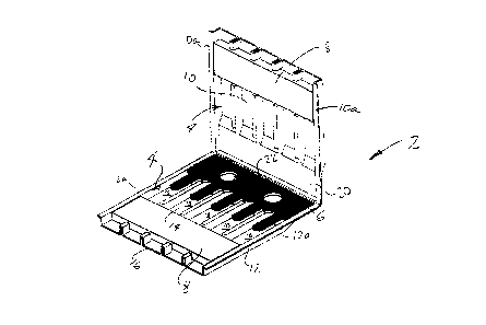
Referring now to the drawings, Figs. 1 and 2 illustrate an electrical interconnection
device 2 inclll~ling a body 4, an electrical element 6 and a sealing member 8.
CA 02226732 l998-0l-l3
W O 97/03481 PCTrUS96/06377
- Body 4 comprises a first section 10 and a second section 12 bonded together along
edges lOa, 12a to form an enclosure 14 having an open edge 16. Enclosure 14 includes
passageways 18 ~o~rten~ling from open edge 16 for receiving a s~lbstr~t~ such as a wire, to a
~7 ret~inin~ portion 20 of the ~nrlosllre. Electric~l element 6 is retained within enclosure 14 in
~ g portion 20. Sealing member 8 is located in enclosure 14 ~dj~c~ont open edge 16, at
the opposite end of passageways 18 from the electrical element.
Sections 10, 12 are preferably constructed of multiple layers of polymeric film, more
preferably P~rp~ntlecl film bonded together to form ~n- losllre 14. It should be noted, however,
that sections 10, 12 may be a variety of constructions, for example, formed, molded or
extruded parts. Prior to bonding sections 10, 12 together, electrical element 6 and sealing
member 8 are inserted into enclosure 14 so as to be sealed therein when the sections are
bonded together. In the ~l~f.,.l~d embodiment, sections 10, 12 are mirror images of each
other, formed integrally with each other along a common edge 22. The sections are folded
over each other at common edge 22, which aids in ~ligning the sections along edges lOa, 12a
with each other so as to mate perfectly, thereby forming enclosure 14, including passageways
18 and ret~inin~ section 20.
Unless restrained by passageways 18, open edge 16 preferably has a configurationsuch that at least one ~limen~ion is smaller than a corresponding ~limen~ion of electrical
el~nnent 6. In this way, the electrical element is retained within enclosure 14. ~It~rn~tively~
i.l~el~;olmection device 2 may have more than one open edge through which substrates may be
inserted for connection to electrical element 6. For example, the interconnection device may
include open edges facing in opposite directions such that substrates may be inserted from
multiple directions or electrical elenn~nt~ may be oriente~ such that open edges are st~
Electrical element 6 may be any electrical joining device, such as a splice, a ground, a
~ circuit protection device, a printed circuit device, or any of a number of electrical elements
for which it is desirable to connect ~u~ dLes thereto. Electrical element 6 is placed in
l~ -g portion 20 prior to bonding sections 10, 12 together, as ~ cll~ed above. The
configuration of electrical eleTnent 6, enclosure 14 and ret~ining portion 20 are such that once
CA 02226732 1998-01-13
WO 97/03481 PCTrUS96/06377
sections 10, 12 are bonded together, the electrical element cannot be removed from the
enc,lc-sllre.
Electrical elemPnt 6 is ~l~rc;lably relatively flat when sealed illl~..;ollllection device 2
S has only a first and second section; how~:~.,., body 4 may be constructed of more than two
sec.ti~nc, such that the electrical element may have a more three ~iim~-n~ion~l configuration.
Additionally, mllltirle electric~l elements may be included in enrlosllre 14. Multiple
elec.trir~l elennent~ may or may not be isolated from every other electrical element.
Sealing element 8 may be any sealing m~teri~l, for example, a gel as described below,
a hot melt adhesive seal as described in U.S. Patent No. 4,972,042 to Seabourne et al issued
on November 20, 1990; or sealed by in~11lrtinn heating as described in U.S. Patent No.
5,378,879 to Monovoukas issued on January 3, 1995. The ~ closllres of each of these
patents is incorporated herein by reference for all purposes. Sealing elemt?nt 8 is placed in
15 enclosure 14 at the end of passageways 18 prior to bonding the body sections together.
Passageways 18 are ~lb~ .ti~lly free of sealing material. As discussed above,
i.lt~lcol~.ection device 2 is relatively small. Sealing member 8 has a m~i...uu. thickness (the
~lim-on~ n through which a :iUb~ dtt: passes when inserted into the device through
passageways 18) of 0.5 inches, preferably not larger than 0.25 inches, and most preferably not
20 larger than 0.12 inches.
The pl.,fe..ed embodiment employs gel as a sealing m~t~ri~l Gels are desirable
because their pl~ p~ . lies allow rcse~ling and reuse. The composition is preferably obtained by
blending at least one prepolymer with an r~trn~l~r and a particulate filler, and then subjecting
25 the blend to con(1ition~ which convert the prepolymer into gel. The gel is a ~ul~sk1lltially
dilute crosslinked system which exhibits no flow when in the steady-state. The crns~link~,
which provide a continuous network structure, may be the result of physical or rllemic~l
bonds, crystallites or other junctions, and must remain intact under the use conditions of the
gel. Most gels c- mpri~e a fluid-e~ten~led polymer in which a fluid, e.g., an oil, fills the
30 intrrstires of the llt;twolh.
_
CA 02226732 1998-01-13
W O 97/03481 PCT/U'_5/.J~77
Gels useful in the present invention include those comrri~ing silicone, for example, a
polyorganosiloxane system, poiyurethane, polyurea, anhydride polymer cont~ining gels such
as anhydride modified EPDM, styrene-butadiene copolymers, styrene isoprene copolymers,
styrene-(ethylene/propylene)-styrene (SEPS) block copolymers (available under the
S tr~-lPn~me SeptonTM by Kuraray), styrene-(ethylene-propylene/ethylene-butylene)-styrene
block copolymers (available under the tr~lPn~me SeptonTM by Kuraray), and/or styrene-
(ethylene/butylene)-styrene (SEBS) block copolymers (available under the tr~cl.on~me
KratonTM by Shell Oil Co.).
Suitable ~t~n~1lor fluids include mineral oil, vegetable oil, p~drr~ c oil, silicone oil,
pl~ tici7~r such as trimellitate, or a nlixtule of these, generally in an amount of 30 to 90% by
weight, based on the total weight of the gel. The gel may be a thermosetting gel, for ~Y~mrle
silicone gel, in which the cros~linke are formed through the use of mllltifimctional
croselinkin~ agents, or a thermoplastic gel, in which micr~hase se~ n of domains serves
15 as junction points. Disclosures of gels which may be suitable as the polymeric co~ ollent in
the composition are found in U.S. Patent Nos. 4,600,261 to Debbaut, 4,690,831 to Uken et al,
4,716,183 to Gamarra et al, 4,777,063 to Dubrow et al, 4,864,725 to Debbaut et al, 4,865,905
to Uken, 5,079,300 to Dubrow et al, 5,104,930 to Rinde et al, and 5,149,736 to Gamarra, and
in Tnt~orn~tional Patent Publication Nos. WO 86/01634 to Toy et al, WO 88/00603 to Francis
et al, WO 90/05166 to Sutherland, WO 91/05014 to Sutherland, and WO 93/23472 to
T-T~mmond et al and U.S. Patent application Serial No 08/379,859 to Mercer et al filed on
January 27, 1995. The disclosure of each of these patents and publications is incorporated
herein by reference.
In addition, the composition may include fillers or collvellLional additives, including
stabilizers, pi~m~nt~, cros~linking agents, catalysts and inhibitors.
Sealing member 8 may be formed as a single piece of gel, or may c- mpri~e two ormore precured pieces. In the most plcrcllcd embodiment, a joint line is formed between two
pieces of gel. The joint line is preferably oriented such that a ~ub~LldLe is insertable into
passageways 18 through the joint line.
A locking means 24 may be employed for locking substrates into interconnection
device 2. Locking means 24 may be heat deformation of a portion of body 4 or may include
physical locking means such as a me-h~nic~lly locking feature formed as part of body
sections 10, 12 or an additional element ca~LivdLcd in passageways 18.
CA 02226732 1998-01-13
W O 97/03481 PCT~US96/06377
In use, sealed interconnection device 2 is provided for connection of substrates 26 to
elect~c~l el~n~Pnt 6. As described above, device 2 is constructed with electrical elem~.nt 6
and sealing member 8 sealed within ~nrlosllre 14. One or more ~ub~Lldles 26 are inserted into r
S passageways 18 through open edge 16 and sealing member 8 and cnnn~cte~l to electrical
elemPnt 6. Sub~LIdles 26 may be of any size, so long as they are capable of being inserted
into device 2 through passageways 18.
A sealing member formed of gel will seal around substrates 26 as the substrates are
10 inserted through the sealing member into enclosure 14. A sealing member formed of a hot
melt adhesive seal or m~teri~l sealed by induction heating must be subjected to the additional
step of a ;liVdLi-lg the sealing member by applying heat or subjecting to a m~gnPtic field, as
a~ L~.
Substrates 26 may be locked in place by applying heat to a portion of body 4 so as to
deform a portion of the body and locking the substrates in place. For example, a hot bar may
be pressed against a portion of at least one of sections 10, 12, to deform the section, thereby
locking substrates 26 in place. ~ltern~tively, the act of inserting substrates 26 into enclosure
14 may activate physical locking means to prevent removal of a substrate, or a&esive, if
20 present for any purpose, may be employed to bond the s~lbstr~t~? in place.
The present invention thus connects the substrates to electrical element 6 using a
small sealed electrical interconnection device.
Variations and modifications can be made to the present invention without departing
from the scope of the present invention, which is limited only by the following claims.