Note: Descriptions are shown in the official language in which they were submitted.
CA 02227179 1998-01-16
COPPER FOIL FOR THE MANUFACTURE OF PRINTED CIRCUITS AND METHOD OF PRODUCING
SAME
FIELD OF THE INVENTION
This invention relates to a method of protecting the surface of copper
foil against tarnishing and oxidation, and to electrodeposited copper foil
suitable for use in the manufacture of printed circuit boards, especially
multilayer printed circuit boards.
BACKGROUND OF THE INVENTION
The production of copper foil for electronic applications, e.g.,
copper-clad laminate for printed circuit boards, involves the use of a
well-known electrodeposition process. This process utilizes a large
cylindrical drum cathode which rotates, partially immersed in a copper
sulfate-sulfuric acid electrolyte. The drum cathode is adjacent to and
facing toward a pair of curved anodes, which may be formed of lead,
lead-antimony, platinized titanium, iridium or ruthenium oxides. Both the
drum and the anodes are connected electrically by heavy buss-bars to a D.C.
power source and currents of up to 50,000 A or more are commonly used. As
the drum rotates in the electrolyte, an electrodeposit of copper forms on
the drum surface, and as the latter leaves the electrolyte, the
electrodeposited copper is continuously stripped from the rotating drum in
the form of thin foil, which is slit to size and wrapped around a take-up
roll. The top surface of the drum is usually formed of stainless steel,
titanium or chromium.
Foil produced in such a process, prior to being treated, is usually
referred to as raw foil. The raw foil is pale pink in color and has two
distinctly different looking sides - a "shiny side", the side which was
plated onto the drum surface and then stripped is quite smooth while the
other side, the side which was facing toward the electrolyte and the anodes,
is referred to as the "matte" side since it has a velvety finish. The matte
side can be imagined as a set of closely packed cones having heights from
three to ten microns, the cone heights depending upon the independent
variables of foil thickness, current density, solution composition, and the
like. This provides the basic shape of the foil surface for embedding in the
resin of a substrate to promote adhesion in the copper-clad laminates used
in the manufacture of printed circuit boards (PCBs).
CA 02227179 1998-01-16
While the matte side of the foil has a certain micro-roughness, a
surface bonding treatment is typically applied to the matte side of the raw
foil to ensure adequate bonding strength after the copper-clad laminate is
formed. The term "bonding treatment" is universally used to refer to
changing one or both surfaces of the electroformed foil to make it suitable
for bonding to laminate resins.
The bonding treatment operation is conducted in machines called
"treaters" wherein rolls of raw foil are unrolled in a continuous manner and
fed into the treater by means of driven rollers (similar to the way in which
a web of paper is handled in a printing machine), rendered cathodic by means
of contact rollers and passed in a serpentine fashion through one or more
plating banks, facing, in each tank, a rectangular anode. Each tank has its
own supply of appropriate electrolyte and its D.C. power source. Between the
tanks, the foil is thoroughly rinsed on both sides. The purpose of this
operation is to electrodeposit on at least one side of the foil, usually the
matte side, micro-projections of complex shape which ensure that the foil
will be firmly anchored to the base polymeric materials used in fabricating
the copper-clad laminates.
Peel strength (the force necessary to pull apart the copper foil and
the supporting insulating substrate material) is a characteristic of the
highest importance, since the mechanical support of the circuit elements as
well as the current carrying capability of PCBs is provided by the copper
foil-polymer joint. It is essential that the foil is bonded very tightly and
securely to the substrate and also that such an adhesive joint can withstand
all the manufacturing steps in the fabrication of PCBs without the decrease
of the initial adhesion, which, moreover, should remain constant throughout
the service life of the PCB.
This bonding operation is carried out in laminating plants and
involves heating and cooling cycles. Sheets of copper foil are laid upon
sheets of "prepreg" (e.g., glass fabric impregnated with epoxy resin). Both
materials are placed in a hydraulic press having heated pressing plates, and
the two materials are pressed together under high pressure. At elevated
temperatures the resin liquefies and is forced, by the pressure, to flow
into the micro-irregularities of the foil surface. This is followed by a
second cycle, when both materials are cooled, while the pressure is being
maintained, the resin solidifies in the irregularities of the foil surface
CA 02227179 1998-01-16
and both materials are firmly bonded together with the result that it
becomes very difficult to pull them apart. It is the responsibility of the
matte side of the foil to ensure high peel strength.
The matte side of the finished foil, i.e., the base foil plus
treatment, refers to the combined effect of the micro-topography of the
matte surface of the base foil (electrodeposited at the drum machine) and
the bonding treatment plated upon that surface at the treater machine. Both
are equally important.
Until only a few years ago the main segment of the total output of
PCBs was represented by single-sided and particularly double-sided boards.
Classical copper foil is an ideal material for the manufacture of such
boards.
As shown in Fig. 1, metallographic cross-sectioning of copper base
foil 10 reveals that the foil's two opposing surfaces are not the same.
While the surface formed next to the drum 12, the shiny side of the foil is
relatively flat and smooth. even when viewed under great magnification, the
surface formed next to the electrolyte 14, the matte side of the foil, has
micro-peaks and valleys. As shown in Fig. 2, the matte side, after
application of the bonding treatment comprises an extremely dense and
uniform coating of spherical micro-projections 16 which greatly enhance the
surface area available for bonding to the polymeric substrates.
The shiny side of the foil, after the lamination, represents the
processing side of the copper-clad laminate. As such, it serves as a
substrate for image patterning and soldering to ensure the necessary
electrical connections between components. In the fabrication of multilayer
PCBs (MLBs), the shiny side of the foil also serves as a surface to be
treated by chemical means (brown oxide or black oxide treatment) for bonding
purposes.
Although many properties of the copper foil are important in the
fabrication of rigid single or double-sided PCBs, the peel strength is one
of the most important. It has to be remembered that copper cladding
constitutes the external surface of the laminate. and that thin copper foil
lines can be relatively easily lifted off the surface of the insulating base
material if the peel strength is not excellent.
CA 02227179 1998-01-16
This is why copper foil manufacturers take advantage of the "natural"
micro-roughness of the matte surface of the base foil, which at that stage
already has a potential "bondability" to polymers, and further enhance it
with bonding treatment to achieve the highest possible final peel strength.
This is not necessary, or indeed a desirable characteristic of copper foil
if it is destined for the manufacture of multilayer boards, which now
dominate the PCB market. In the case of the inner layers of MLBs, copper
foil is encapsulated or "sandwiched" between the layers of prepreg, and
moreover, the double-sided laminates for inner layers are quite thin. That
raises the need for "low-profile", "not-too-high peel strength" copper foil
so that the laminate's dielectric properties are not adversely affected,
which frequently is a result of excessive bonding treatment.
On the other hand, the fact that the top side (shiny side of the foil)
is laminated against a prepreg that separates it from the next inner layer
raises the question of reliability of such an adhesive joint. The shiny side
of the foil is quite smooth and offers little "bondability." This is why
manufacturers of MLBs apply a so-called oxide treatment to the top side of
copper tracks, to enhance their bondability.
It is widely accepted practice in the manufacturing of MLBs to use
oxidation techniques to promote the adhesion between the copper surface of
the inner layers and the prepreg. Without oxide treatment, the bond between
copper and the prepreg layer is insufficient to withstand the thermal shock
of reflow soldering.
During the formative years of the multilayer board industry, with
relatively less dense patterns of the inner layer circuitry, the bond
between the prepreg and the base laminate of the inner layers was not
considered important. It was believed that copper tracks could be
encapsulated in the cured prepreg. On the other hand, today's internal
circuitry is very dense and most of the bonding is to copper rather than to
base laminate. Today, the surfaces of copper tracks have to be
"adhesion-prone".
The oxide treatment techniques used in the fabrication of MLBs are
troublesome, expensive and create their own technical problems. One is the
so-called "pink ring" which results from the chemical attack on copper oxide
layers by the chemicals used in through-hole plating. It is customary now
CA 02227179 1998-01-16
.
to use additional steps of brown oxide treatment, which involves the
reduction of cupric oxide to metallic copper, since the bonding treatment
with copper is immune to pink ring, as opposed to CuO which is easily
dissolved in mineral acids. This reduction step further complicates brown
oxide processes and renders them even more expensive.
It has been proposed that a special copper foil provided with the
bonding treatment on the shiny side of the foil is better suited to the
fabrication of MLBs. If the bonding treatment is plated onto the drum side
of the foil this results in a lower peel strength (e.g. about 1.4 N/mm (8
lbs./inch)) than when the same treatment is plated onto the matte side of
the foil (e.g. about 2.1 N/mm (12 lbs./inch)). Nevertheless, such peel
strength is more than adequate in MLBs.
With respect to copper foil destined for use in producing MLBs, we
have found that the brown oxide treatment which is presently applied to the
shiny side of the foil and provides a quite low peel strength can
advantageously be applied to the matte side of base foil, which by itself,
due to its peak and valley topography and the resulting micro-roughness, has
a considerable peel strength of about 0.7 N/mm (4 lbs/inch), as opposed to
the shiny side of the foil, which has substantially no peel strength at all.
When this is done, very little brown oxide has to be applied to the matte
side of the foil to bring the peel strength to the desired level of, for
example, 1.23 N/mm (7 lbs/inch) or so. This reduced amount of brown oxide
is much less fragile in terms of structure, than the greater amount of brown
oxide that has to be applied to the shiny side of the foil to achieve the
same peel strength. The need for reduction of cupric oxide to metallic
copper can thus be eliminated, and the entire process becomes simpler and
less expensive, while the quality of MLBs (particularly the dielectric
properties and the resistance to delamination due to solder shock) are
improved.
However, the change in the process of manufacturing this special
copper foil, when compared to the classical process, requires more than the
mere application of bonding treatment to the shiny side, rather than to the
matte side, of the base foil.
Since the matte side of this special foil will first be subjected to
"imaging" when a circuitry pattern is transferred to a panel, and then to
CA 02227179 1998-01-16
.
brown oxide treatment, the usual method of "stainproofing" the matte side
to protect it from tarnishing and oxidation should be reformulated to render
it more suitable for use in commercial operations.
Brown oxide treatment for MLBs and micro-etching techniques have in
common the property that either a sodium chlorite or a sulfuric acid
peroxide micro-etching solution must reach the surface of the copper to
produce uniformly the desired reaction or effect. Stainproof layers,
therefore, have to be either easily removed by precleaning solutions or be
easily penetrable by brown oxide or micro-etch liquids. Excessively
tenacious stainproof layers can form an impenetrable shield between the
surface of copper and the processing chemicals, delaying the desired
reactions or producing obvious non-uniformity.
With the advent of miniaturized electronics, very densely packed
printed circuit boards are needed. Miniaturization often requires that the
copper foil conductor, or track lines, of today's printed circuit board be
as narrow as 127 microns (5 mils) or less. The degree of high definition of
fine-line circuitry depends on the quality of copper foil manufactured for
the electronic industry, particularly on the surface quality of both sides
of the foil.
It is the practice in the manufacture of printed circuit boards from
copper-clad laminate to form the image of the desired printed circuit
pattern on the copper surface of the laminate by a photographic technique,
which leaves the desired pattern formed of a photoresist material on the
surface of the copper. For the photographic imaging to be sharp and precise,
photoresist has to spread well on the foil's surface and adhere well to it.
It is a practice in the manufacture of printed circuit boards to
roughen the surface of the shiny side of the copper foil to achieve good
resist adhesion. This roughening also removes tenacious stainproof films
which foil manufacturers apply to the foil to protect it from oxidation and
staining before it reaches the user. Photoresist does not adhere to the
stainproof films, which therefore have to be removed. Thus, roughening of
the foil surface serves the purpose of removal of stainproof film as well
as changing the copper surface topography from smooth to micro-rough, to
facilitate photoresist adhesion, which is a condition of good definition of
track lines.
CA 02227179 1998-01-16
This roughening is performed either by mechanical means (e.g. abrasion
by brushes, scrubbing with pumice) or chemical means (so-called
micro-etching), which is accomplished by subjecting the copper surface of
copper-clad laminates to the etching action of oxidizing mineral acids. Such
acids attack the smooth surface of the foil along the copper grain
boundaries, thus creating pits and pores and change the copper surface from
smooth to micro-rough.
In the fabrication of MLBs, copper foil is laminated (bonded to
polymeric substrates twice). First, thin, double-sided copper-clad laminates
are produced. These laminates are then subjected to image patterning and
etching away of unwanted copper to produce the desired patterns of
circuitry. Several layers of double-sided boards prepared in such a manner
are stacked together, with sheets of prepreg inserted in between to separate
dielectrically each inner board from the other. Such a stack of circuit
boards and prepreg is then laminated together to form a monolithic
multilayer board. Later, holes are punched or drilled through the board in
prearranged places and so-called through-hole plating of copper is used to
ensure the electrical interconnection between all layers of copper-track
conductor lines.
Good bonding is required between the top surfaces of track lines (the
surface which was used for image patterning) and the sheets of prepreg, in
the course of second (so-called B-stage) lamination.
It is a practice in the fabrication of MLBs to subject the inner layer
boards, with their patterns of circuitry. to the so-called brown oxide
treatment, which changes the micro-topography of the top surfaces of the
track lines to improve their bondability to the polymeric prepreg. This
brown oxide treatment is produced by immersing the boards in an alkaline
solution of sodium chlorite which, by its oxidizing action, causes the
conversion of metallic copper on the top surfaces of exposed copper tracks
into cupric oxide (CuO), possibly in an admixture of cuprous oxide (Cu2O),
depending on the type of the bath and operating conditions. This oxide
coating grows in the form of dendritic crystals, perpendicular to the
surface of the copper tracks. Thus, the surface area available for bonding
to polymeric substrates is increased and improved bondability is achieved.
CA 02227179 1998-01-16
Various patents directed to bonding treatments for copper foil
disclose that one or both sides of the foil which is to be bonded to the
substrate is subjected to bonding treatment (U.S. Patent 5.207.889), or that
treatment for copper foil that is to be used for lamination to a board
comprises electrodepositing a dendritic layer of copper followed by a
gilding layer of copper on the side of the foil that is to be laminated to
the board (U.S. Patent 4.572.768). Also, the use of either the shiny or
matte side of the foil to achieve flexibility in terms of surface
characteristics of the resulting copper-clad laminates. which have either
a mirror-like shiny side or "copper-clad laminate having a satin finish"
(matte side) is disclosed in U.S. Patent No. 3.998.601. U.S. Patent No.
3.857.681 discloses the application of copper dendritic and gilding layers
to at least one of the surfaces of copper foil to improve the bond strength
when laminated to a polymeric substrate. followed by the application of a
zinc coating to prevent laminate staining or discoloration.
US patent 5.071.520, which forms the basis for the preamble of
appended claim 1, discloses a method of treating metal foil to improve peel
strength and discloses a copper foil suitable for use in the manufacture of
printed circuit boards. The foil comprises an electrodeposited copper base
foil having a matte surface and an opposing shiny surface and discloses the
use of an oxidation-and-tarnish-resistant protective layer provided on one
surface and the use of an electrodeposited bonding treatment provided on the
opposing surface.
The application of a stainproofing chromate layer on the surface of
copper foil to protect against tarnish and oxidation. as disclosed in U.S.
Patent Nos. 3.625.844 and 3.853.716, is also known.
The matte side of the foil, with its own micro-roughness and the
resulting bondability. is a better surface upon which to grow the layer of
brown oxide, than the traditionally used shiny side of the foil, even if it
is roughened by either micro-etching or mechanical abrasion.
SUMMARY OF THE INVENTION
It is the general object of the present invention to provide a method
of controlling the surface characteristics of the matte surface of copper
foil to make it particularly suitable for high-resolution image patterning,
CA 02227179 1998-01-16
and also a method of providing the matte surface with a stainproofing layer
which in the course of fabrication of printed circuit boards can be easily
removed by dissolution in aqueous solutions of alkalis. Other objects and
advantages of the present invention will become apparent from the following
description thereof and from the practice of the invention.
To achieve the objects of the present invention there is provided a
method for protecting the surface of copper foil against tarnishing and
oxidation as described in the appended claims.
In accordance with the present invention, the matte side of the foil
is provided with a stainproofing layer (derived from the stainproofing
electrolyte and applied electrolytically to the foil's surface) which, while
protecting the foil from oxidation prior to the foil's use, can be easily
removed from the surface of copper-clad laminate by simple immersion in a
dilute alkaline solution such as aqueous sodium or potassium hydroxide at
a low temperature (e.g. about 8 lbs./inch and approximately ambient),
without the need for brushing, scrubbing or micro-etching.
The purpose of the stainproofing process in the manufacture of copper
foil is to form on the surface of the foil a protective coating which
extends the shelf-life of the foil by protecting it against atmospheric
oxidation as well as from oxidation at elevated temperatures used during the
laminating processes by which copper-clad laminates are fabricated.
The stainproofing layer which protects the copper foil against
oxidation has functions other than just extending the shelf-life of the
foil. Once the copper-clad laminates are ready for further processing, the
protective layer has to be easily removed from the image patterning side of
the foil by quick and complete dissolution in alkalis, since the complete
removal of stainproofing compounds is required to assure good adhesion of
photoresists, unhindered response to the etchants and good acceptability of
brown oxide treatment. Thus, the type, structure, chemical composition and
the thickness of the stainproofing layer that protects the "processing" side
(the side subjected to imaging) of the foil is extremely important.
The present invention takes advantage of the fact that copper foil
produced by means of electrodeposition on a rotating drum cathode possesses
two top surfaces which are not the same. While the surface next to the drum,
CA 02227179 1998-01-16
the shiny side of the foil, even when viewed under great magnification, is
relatively flat and smooth, the surface next to the electrolyte, the matte
side of the foil, is already micro-rough (viewed under a high-resolution
electron microscope, the surface is seen to be composed of micro-peaks and
micro-valleys). Moreover, the degree of micro-roughness can be controlled
in this case by the manufacturer of copper foil much better than when
mechanical or chemical roughening is carried out by the manufacturer of
printed circuit boards.
Thus, a laminate produced by bonding foil matte-side-up to the
polymeric material assures excellent photoresist adhesion and thus a high
degree of fine-line precision of definition. The bonding treatment applied
to the shiny side (or drum side) of the foil assures good anchoring of track
lines to the polymeric substrates.
There is a further advantage of the present invention that results
from fabrication of the copper foil with the bonding treatment applied to
the shiny side of the foil and using the matte side for the image
patterning. This advantage lies in the fact that such foil is particularly
well adapted for use in the manufacture of MLBs which now dominate the
printed circuit board market, because they can achieve the highest
functional density of circuitry in electronic packaging.
BRIEF DESCRIPTION OF THE DRAWINGS
The following description of the present invention will be better
understood by reference to the accompanying drawings, which form a part
hereof. In the drawings:
Fig. 1 illustrates conventional copper base foil;
Fig. 2 illustrates conventional finished copper foil having a bonding
treatment applied to the matte side thereof; and
Fig. 3 illustrates copper foil in accordance with the present
invention.
DESCRIPTION OF THE INVENTION AND A PREFERRED EMBODIMENT THEREOF
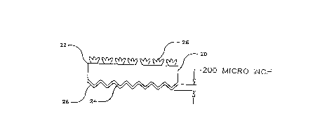
Referring to Fig. 3, finished copper foil in accordance with the
present invention comprises an electrodeposited copper base foil 20 having
a matte surface 24 on which there is electrodeposited a protective layer 28
CA 02227179 1998-01-16
11
containing zinc and one or more compounds of trivalent chromium, referred
to hereinafter as a chromate or chromates. The foil 20 has a smooth or shiny
side 22 on which there is an electrodeposited bonding treatment 26. The
matte surface of the raw foil preferably has a surface roughness, or Rz (as
hereinafter defined) of from about 3 to about 10, most preferably about 5
microns.
The base foil may be formed by any of the well-known techniques for
producing copper foil, such as the one wherein a thin foil is
electrodeposited from a copper ion-containing electrolyte onto the smooth
surface of a rotating drum cathode partially immersed in the electrolyte and
then stripped from the surface of the drum, slit and rolled. The copper foil
so produced has one surface, on the drum side, which is smooth or shiny and
another surface, on the opposing electrolyte side, which is matte.
In the fabrication of copper-clad laminates for printed circuits,
copper foil is bonded to a polymeric substrate (a composite material such
as epoxy, polyimide or a like resin reinforced with glass fiber fabrics) by
means of mechanical interlocking at the interface between the two materials.
To achieve a high degree of interlocking, the bonding side of the foil
is provided with a bonding treatment. Such treatment consists of an
extremely dense coating of copper spherical micro-projections, which is
electrodeposited to the shiny or smooth (drum) side of the base copper foil.
The peel strength of copper foil (the force necessary to separate, or
pull away the foil from the polymer substrate) will depend on the shape of
the individual micro-projections, their mechanical strength and hardness,
density per surface area and their distribution over the smooth surface of
the drum side of the base foil. In turn, all the factors listed above will
depend on the conditions under which the bonding treatment is
electrodeposited.
The preferred bonding treatment is effected by subjecting the shiny
side of the base or "raw" foil to four consecutive electrodeposition steps.
The first consists of the deposition of a micro-dendritic copper layer which
enhances, to a very large degree, the real surface area of the matte side,
and thus enhances the foil's bonding ability. It is followed by
electrodeposition of an encapsulating, or gilding layer, the function of
CA 02227179 1998-01-16
12
which is to mechanically reinforce the dendritic layer, and thus render it
immune to the lateral shear forces of liquid resins in the laminating stage
of PCB fabrication. Then, a so-called barrier layer is deposited on the
dual-layer copper treatment, after which a stainproofing layer is applied.
The purpose of the dendritic deposit is to increase the "true" surface
area of the shiny side, since that property is ultimately responsible for
the bonding characteristics of the foil. The shape, height, mechanical
strength and the number of dendritic micro-projections per surface area
which constitute the dendritic deposit are the factors instrumental in
achieving adequate bond strength of the foil, after all stages of the
treatment are completed. The dendritic deposit, the first stage of the
treatment, is relatively weak mechanically and given to unacceptable
treatment transfer characteristics.
The encapsulating step of the treatment is very important, since it
eliminates the foil's tendency to "treatment transfer" and the resulting
"laminate staining" which can cause the decrease of the laminate's
dielectric properties. The role of this second treatment stage is to
mechanically reinforce the fragile dendritic layer, by overplating it with
a thin layer of sound and strong metallic copper, which locks the dendrites
to the base foil. Such a dendrite-encapsulation composite structure is
characterized by high bond strength and the absence of treatment transfer.
The treating parameters which assure this are relatively narrow. If the
amount of the gilding deposit is too low, the foil will be given to
treatment transfer. If, on the other hand, the gilding layer is too thick,
a partial loss of peel strength may be expected. These first two layers of
the treatment are composed of pure copper, in the form of microscopic,
spherical micro-projections.
The dual-layer copper bonding treatment may have electrodeposited
thereon a very thin layer of zinc or zinc alloy, a so-called barrier layer.
During the fabrication of copper-clad laminates destined for PCBs, the
zinc-containing layer alloys with the underlying all-copper bonding
treatment by the process of heat-accelerated diffusion of metals in the
solid state. As a result, a layer of chemically stable alpha brass is formed
over the surface of the all-copper treatment. Its purpose is to prevent
direct copper-epoxy resin contact, and this is why the zinc-containing layer
(which during lamination is converted to alpha brass) is referred to as a
CA 02227179 1998-01-16
barrier layer. If the bonding treatment, composed of copper only, is
subjected to lamination with epoxy resin systems, it tends to react with
amino groups of the resin, at the high laminating temperatures. This, in
turn, may create moisture at the foil-resin interface, causing the harmful
effect of "measling", and possibly delamination. The barrier layer plated
over the all-copper bonding treatment prevents these harmful effects.
All three stages of the treatment mentioned above, as is well known
in the art, are effected by means of electrodeposition, which changes the
geometry and morphology of the smooth side of the foil and assures the
mechanical strength of the surface region.
The foil treated as described above may then be subjected to an
electrochemical stainproofing which changes the surface chemistry. As a
result of this step, the bonding surface is rendered chemically stable. This
stainproofing operation removes weak surface films, which can greatly
decrease the adhesion of the foil to the substrate, and provides a stable
film of controlled thickness, responsible for imparting to the treated
surface the "durability" of its properties.
The above bonding treatment, barrier layer and stainproofing may be
applied to the shiny surface of the base foil by the methods disclosed in
U.S. Patent No. 4.572.768 (Wolski et al.), U.S. Patent No. 5.207.889 (Wolski
et al.), U.S. Patent Re 30.180 and/or U.S. Patent No. 3.857.681 (Yates et
al.).
The proper chemical composition and the thickness of the stainproof
layer are very important in achieving a good, easily removable stainproof
layer, while not diminishing its protective ability.
Providing the matte side of the foil with the layer of stainproofing
in accordance with the present invention involves the simultaneous
deposition of chromate ions and metallic zinc, and this is a very unusual
case of alloy plating, since one constituent of the electrolyte, chromic
acid, is reduced at the foil surface (cathode), not to a metallic state, but
to a trivalent state, which in turn enables the formation of a chromate
stainproofing layer on the matte surface 24.
CA 02227179 1998-01-16
14
The stainproofing electrolyte used in the present invention has the
dual function of chromating and zincating, and thus forms the protective
layer of the stainproofing of the present invention, which is also dual in
its protective role, offering both mechanical protection, typical of
conversion coatings, as well as electrochemical (sacrificial) protection,
typical of zinc coatings.
The factor which enables the co-deposition of chromates and metallic
zinc is the pH of the electrolyte. At very low pH values, e.g. a pH of 2
(which is the value for 3 g/l CrO3), hexavalent chromium compounds are very
strong oxidants, thus counteracting the cathodic reduction of zinc. At such
a pH, the standard electrode potential Eo has a value of +1.33 V for the
following reaction:
Cr2O72~ + 14H+ + 6e = 2Cr3+ + 7H2O
and under such conditions co-deposition of zinc is impossible. In basic
solutions, chromates rather than dichromates are the prevailing species, and
are by and large much less oxidizing.
The reaction:
CrO42~ + 4H2O + 3e = Cr(OH)3 + 50 H- Eo = 0.13 V
is much closer to the standard electrode potential of zinc Eo -0.76 and
enables the deposition of the chromates and metallic zinc.
In accordance with the present invention, the bulk of the electrolyte
is moderately acidic, and preferably has a pH value of from about 3 to about
4. 5, most preferably from about 3.5 to about 4 and typically the
electrolyte has a pH of about 4 which is, of course, far from basic, but it
refers to the bulk of the electrolyte. The pH at the foil-solution
interface, however, exceeds 7. Whenever there is a flow of current, there
is necessarily a reduction of some chemical species at the cathode (foil).
In the present process cathodic reactions are:
Reduction of Cr6+ (see above)
Reduction of zinc Zn2+ + 2e = Zn
Reduction of water 2H2O + 2e = 20H- + H2
CA 02227179 1998-01-16
It is the last reaction, i.e., evolution of hydrogen at the foil
surface, which is responsible for the above-mentioned local increase of pH,
thus allowing for simultaneous precipitation of a chromate layer and the
deposition of zinc.
It has been found, by studying the chemical composition of
experimental stainproof layers, using instrumental methods of surface
analysis (scanning auger microprobe, and ESCA (electron spectroscopy for
chemical analysis)), that stainproofing layers capable of good protective
action while also being easily removable by immersion in alkalis, typically
contain about 10-20% of chromium (calculated as metallic chromium) and
20-40% of zinc (calculated as metallic zinc), the balance being water, and
are less than 10 nm (100 A) thick. The ratio of chromium to zinc is very
important. The relatively high zinc content in the layer assures that the
layer is easily dissolved by alkalis; due to the amphoteric character of
this metal it dissolves in sodium hydroxide forming sodium zincate with
copious evolution of hydrogen. Therefore, the stainproofing layer should
have a zinc to chromium ratio (both calculated as the metal) of at least
1:1, and preferably about 2:1, by weight.
Since the atoms of zinc are uniformly dispersed within the lattice of
the chromates, such as the chromium hydroxide component of the protective
layer, alkaline cleaners attack and dissolve atoms of zinc, hydrogen is
formed, and this combined effect of alkaline attack and "fizzing" lifts
chromium compounds off the surface of the foil, leaving it, after the rinse,
pure and clean, and ready for further PCB processing.
The following electrolyte and electroplating conditions may be used
to form the stainproofing layers described above:
ELECTROLYTE
CrO3 - 0,75 grams/liter (g/l) - 2 g/l: preferably 1,25 g/l
Zn (calculated as Zn) - 0,3 g/l - 1,0 g/l; preferably 0,5 g/l
H3PO4 - 0 g/l - 2 g/l; preferably 0,5 g/l
H20 - balance
CA 02227179 1998-01-16
16
ELECTROPLATING CONDITIONS
pH 3,5 - 4,0
T - 32~C (90~F)
Current density - 46 A/m2 (0,5 A/ft2) - 185 A/m2 (20 A/ft2);
preferred 93 A/m2 (lO A/ft2)
Plating time - 1 second to 5 seconds; preferred 3 seconds. The copper
foil is rendered cathodic with respect to the anode, immersed in the bath,
and facing the foil, and thus electrodeposition of the stainproofing layer
is accomplished. The present stainproofing method is an improvement in the
prior stainproofing methods disclosed in U.S. Patent No. 3.625.844 (McKean)
and U.S. Patent No. 3.853.716 (Yates et al.).
It has been found that the ability of the stainproof layer to protect
the "processing" side of the copper foil or the copper-clad laminate from
various forms of oxidation, while maintaining the layer behind easily
removable by chemical means, can be further enhanced by plating on the matte
side of the foil an extremely thin layer of zinc prior to the deposition of
20 the stainproof layer to the same side of the foil.
The explanation of this improvement is as follows: of the two
components of the stainproof layers, zinc assures the resistance of the
copper surface it protects to direct oxidation, due to the heat of the
25 laminating process and the post-bake. In addition, due to its amphoteric
nature, zinc is easily soluble in both mineral acids and alkalis, and thus
contributes toward easy removal of the protective layer by chemical means.
The trivalent chromium component of the layer is responsible for
30 protecting the copper surface against atmospheric or "wet" corrosion and
thus provides the copper foil with a good shelf-life. Chromium compounds,
however, bound chemically to the copper surface, are much less soluble than
zinc in the acids and alkalis, and are therefore much more difficult to
remove by chemical means than the zinc component of the protective layer.
Eventually, the compromise between protective action and cleanability
is reached by the careful choice of the proportion of zinc and chrome
compounds in the stainproof layer and also of the thickness of the
protective film.
CA 02227179 1998-01-16
The nature of the process ensures that the distribution of both
elements and their ratio throughout the thickness of the layer is uniform.
Obviously, the best way of resolving the conflicting requirements of
protection and removability aspects of the stainproof layer would be if the
depth profile of this layer favored zinc right next to the surface of the
metallic copper, for the first 2 nm (20 A) or so of the total 10 nm (100 A)
thickness of the stainproof layer. The remaining 8 nm (80 A) of the layer,
toward its outer perimeter, should consist of the zinc composite and the
compounds of trivalent chromium in the proportions described previously.
If the thin coating of the metallic zinc, without chromium compounds,
is immediately adjacent to the surface of the metallic copper, the ability
of zinc to sacrificially protect copper against direct oxidation is even
better than the protective ability of the stainproof film alone.
Similarly, the presence of a pure zinc coating next to the copper
surface further facilitates the easy and complete removal of the protective
film by chemical cleaners.
The deposition of the very thin coating of metallic zinc prior to the
deposition of the stainproof layer is effected in a separate plating tank
of the treater machine by a cathodic process. The foil is rendered cathodic
in the said tank. An anode faces the processing side of the foil. The
electric circuit is thus completed and, by controlling the amount of flowing
current, the desired thickness of zinc coating can be deposited onto the
copper surface. This coating is then followed by the deposition of a
stainproof layer in the next plating tank of the treater machine.
If desired, the same stainproofing may also be applied to the shiny
side of the foil having the above-described bonding treatment.
The bonding treatment plated onto the drum or shiny side of the foil
results in lower peel strength than the same bonding treatment plated onto
the matte side of the foil (about 1.4 N/mm (8 lbs/inch) rather than 2.1 N/mm
(12 lbs/inch)). Nevertheless, such lower peel strength is more than adequate
in MLBs. On the other hand, when the brown oxide treatment, presently
applied to the shiny side of the foil and supplying quite low peel strength,
is applied to the matte side of the base foil (which by itself, due to its
CA 02227179 1998-01-16
18
peak and valley topography and the resulting micro-roughness has a
considerable peel strength of about 0.7 N/mm (4 lbs/inch), as opposed to the
untreated shiny surface of the foil, which has substantially no peel
strength at all), relatively little brown oxide has to be applied to the
matte surface of the foil to bring the peel strength to the desired level
of about 1.05 N/mm (6 lbs/inch). This reduced amount of brown oxide is much
less fragile in terms of structure, than the greater amount of brown oxide
that is presently applied to the shiny surface of the foil to achieve the
same peel strength. When the matte surface of the foil is subjected to the
brown oxide treatment, the need for reduction of cupric oxide to metallic
copper is eliminated, and the entire process becomes simpler and less
expensive, while the quality of the MLBs (particularly the dielectric
properties and the resistance to delamination due to solder shock) are
improved.
When the shiny surface of the copper foil is used as the processing
side of the foil, cleaning and roughening of the surface prior to resist
(both etch resist and plating resist) application is critical. Since there
is less surface area for the resist to cling to, that surface must be at an
optimum state in order for the resist to adhere and provide a successful
etch. An area where the resist lifts at the edge of a circuit trace or where
there is a deep gouge that the resist does not fully cover could mean an
etched-through trace which may require expensive repair or even the
scrapping of the board altogether. Such cleaning and roughening of the
process side of the copper foil is accomplished by the use of the well-known
mechanical scrubbing and micro-etching techniques, the need for which is
obviated by copper foil in accordance with the present invention.
The following example describes a preferred embodiment of the present
invention and demonstrates certain advantages thereof.
EXAMPLE
A web of base (or raw) foil, 35 microns thick (so-called one-ounce
foil in terms of weight per surface area), was produced by means of
electrodeposition of copper on a rotating drum cathode, using the
electrolyte, grain-refining agents and plating parameters described in
column 17 of U.S. Patent No. 5.215.646 (Wolski, et al.), except that only
primary anodes. and not the secondary anode. were used.
CA 02227179 1998-01-16
19
This base foil had one top surface which was smooth or shiny, and
another opposite top surface which was matte because of its complex
micro-topography. The second surface was composed of micro-peaks and
micro-valleys, which together formed the matte side's micro-roughness. The
matte side of the foil was examined for micro-roughness (by a stylus-type
instrument) and was found to be 5,3 microns (210 micro-inches).
The base foil described above was, in turn, passed through a treater
machine in order to provide the shiny side of the foil with a multilayer
(copper dendritic layer, copper gilding layer and a barrier layer) bonding
treatment, and to provide the matte side of the foil with an easily
removable stainproofing layer.
This multilayer bonding treatment applied to the shiny side of the
foil employed the techniques, plating parameters and the electrolytes
described in U.S. Patent No. 4.572.768 (Wolski et al.), to produce a treated
side.
The matte side of the foil was provided with an easily removable (by
means of dissolution in 5% solution of sodium or potassium hydroxide)
stainproofing film. The technique of electrolytic copper stainproofing
process used was based on U.S. Patent No. 3.853.716 (Yates et al.). using
an electrolyte comprising:
CrO3 - 1,0 g/l
Zn (added as ZnSO4) - 0,4 g/l
H3PO4 - 0,5 g/l
H2O - balance
pH - 3,9
T - 32~C (90~F)
The stainproofing layer was deposited electrolytically on the matte
side of the foil (which was used as a cathode), employing a current density
of 18.5 A/m2 (2A/ft2) and a plating time of 1,5 seconds. The resulting
stainproofing layer was examined and found to comprise metallic zinc and
chromates and to have a zinc to chromium ratio of 1,85:1,0.
The copper foil produced in the manner described above was then
subjected to the following tests:
CA 02227179 1998-01-16
The copper foil was laminated (bonded) to a prepreg (composite
material of glass fiber fabric and epoxy resin) designated F M by the
National Electrical Manufacturer's Association (NEMA) in two variants:
1. treated-side-down,
2. matte-side-down.
The peel strength of each of the treated sides and the matte side of
the prepreg was then measured. The peel strength of the shiny side of the
foil with the bonding treatment was found to be 1.7 N/mm (9.8 lbs/inch) of
width of laminate. while the peel strength of the matte side of the foil was
found to be 0.74 N/mm (4,2 lbs/inch).
Another matte-side-up laminate was prepared as described above and the
"cleanability" of the matte surface was examined. The laminate was first
immersed for 30 seconds in 5% solution of sodium hydroxide. at room
temperature and then thoroughly rinsed. The laminate was then immersed in
a commercial brown oxide solution. a solution manufactured by Mac Dermid
Company, 9804/9805 bronze oxide. The pink colored matte side of the copper
immediately acquired a deep brown color, due to the reaction of copper with
sodium chlorite which is the main constituent of the brown oxide solution.
This indicates that this stainproofing film was completely removed by
immersion in the solution of sodium hydroxide and that the stainproofing
layer was easily removable. If the stainproofing layer had not been removed,
the pink colored matte side would not have reacted with the brown oxide
solution, and the deep brown color of cupric oxide would not have appeared
on the copper surface.