Language selection

Search

Patent 2227313 Summary

Third-party information liability

Some of the information on this Web page has been provided by external sources. The Government of Canada is not responsible for the accuracy, reliability or currency of the information supplied by external sources. Users wishing to rely upon this information should consult directly with the source of the information. Content provided by external sources is not subject to official languages, privacy and accessibility requirements.

Claims and Abstract availability

Any discrepancies in the text and image of the Claims and Abstract are due to differing posting times. Text of the Claims and Abstract are posted:

  • At the time the application is open to public inspection;
  • At the time of issue of the patent (grant).
(12) Patent Application: (11) CA 2227313
(54) English Title: METHOD AND APPARATUS FOR IMPROVING ERROR PATH CONTROL IN A FEED-FORWARD AMPLIFIER
(54) French Title: COMMANDE DE CHEMIN D'ERREUR DESTINEE A UN AMPLIFICATEUR A CORRECTION AVAL
Status: Deemed Abandoned and Beyond the Period of Reinstatement - Pending Response to Notice of Disregarded Communication
Bibliographic Data
(51) International Patent Classification (IPC):
  • H03F 01/00 (2006.01)
  • H03F 01/32 (2006.01)
(72) Inventors :
  • VAN HORN, MARK IAN (United States of America)
(73) Owners :
  • MOTOROLA, INC.
(71) Applicants :
  • MOTOROLA, INC. (United States of America)
(74) Agent: GOWLING WLG (CANADA) LLP
(74) Associate agent:
(45) Issued:
(86) PCT Filing Date: 1997-02-13
(87) Open to Public Inspection: 1997-11-27
Examination requested: 1998-01-15
Availability of licence: N/A
Dedicated to the Public: N/A
(25) Language of filing: English

Patent Cooperation Treaty (PCT): Yes
(86) PCT Filing Number: PCT/US1997/002367
(87) International Publication Number: US1997002367
(85) National Entry: 1998-01-15

(30) Application Priority Data:
Application No. Country/Territory Date
08/649,357 (United States of America) 1996-05-17

Abstracts

English Abstract


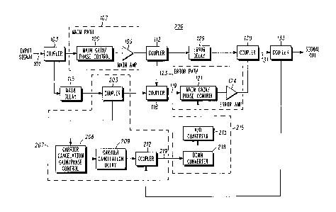
A feed-forward amplifier (200) bases control of an error path (123) within the
feed-forward amplifier (200) on an output signal after performing carrier
cancellation to remove the carrier signal. The feed-forward amplifier (200)
implements couplers (203, 212), a carrier cancellation gain/phase control
block (206) and a carrier cancellation delay block (209) to cancel the carrier
signal. By basing the control of the error path on a signal without the
carrier signal, control of the error path (123) does not suffer from the
effects of high dynamic range presented by the carrier signal, thus improving
overall control of the feed-forward amplifier (200).


French Abstract

Cet amplificateur à correction aval (200) base la commande d'un chemin d'erreur (123) sur un signal de sortie, après avoir annulé la porteuse afin d'enlever le signal de celle-ci. Cet amplificateur (200) met également en oeuvre des coupleurs (203, 212), un bloc de commande (206) de gain/phase d'annulation de la porteuse, ainsi qu'un bloc de temporisation (209) d'annulation de la porteuse, afin d'annuler le signal de la porteuse. En basant la commande du chemin d'erreur (123) sur un signal dépourvu du signal de la porteuse, cette commande ne subit par les effets du champ dynamique élevé présenté par le signal de la porteuse, améliorant ainsi la commande globale de l'amplificateur (200) à correction aval.

Claims

Note: Claims are shown in the official language in which they were submitted.


7
Claims
1. A method of improving error path control in a
feed-forward amplifier, the feed-forward amplifier having a
main path and the error path and amplifying a carrier
signal for transmission to a destination, the method
comprising the steps of:
canceling the carrier signal from a signal output from
the feed-forward amplifier to produce a control signal; and
controlling the error path of the feed-forward
amplifier based on the control signal.
2. The method of claim 1, wherein the step of controlling
the error path further comprises controlling the amplitude
and phase of an input error signal.

3. An apparatus for improving error path control in a
feed-forward amplifier, the feed-forward amplifier having
a main path and the error path and amplifying a carrier
signal for transmission to a destination, the apparatus
comprising:
means for canceling the carrier signal from a signal
output from the feed-forward amplifier to produce a
control signal; and
means for controlling the error path of the
feed-forward amplifier based on the control signal.
4. The apparatus of claim 3, wherein the means for
canceling the carrier signal further comprises, in series, a
first radio frequency (RF) coupler, a carrier cancellation
gain/phase control block, a carrier cancellation delay block
and a second RF coupler.
5. The apparatus of claim 3, wherein the means for
controlling the error path of the feed-forward amplifier
based on the control signal further comprises a
downconverter and an analog-to-digital (A/D) converter.
6. The apparatus of claim 5, wherein the
analog-to-digital (A/D) converter further comprises, at most, an 8-bit
analog-to-digital (A/D) converter.

9
7. A feed-forward amplifier for use in a wireless
communication system, the feed-forward amplifier
comprising:
a main path for amplifying an input signal having a
carrier signal and an error signal;
an error path, coupled to the main path, for adjusting
the error signal;
a carrier cancellation block, having as an input a
signal output from the feed-forward amplifier, for
canceling the carrier signal from the signal output from the
feed-forward amplifier to produce a control signal; and
a controller, coupled to the carrier cancellation block,
for controlling the error path utilizing the control signal.
8. The feed-forward amplifier of claim 7, wherein the
controller for controlling the error path further comprises a
controller for controlling the amplitude and phase of an
error signal input into the error path.
9. The feed-forward amplifier of claim 7, wherein the
controller further comprises a downconverter and an
analog-to-digital (A/D) converter having, at most, 8-bit
resolution.

10. A feed-forward amplifier for use in a wireless
communication system, the feed-forward amplifier
comprising:
a main path for amplifying an input signal having a
carrier signal and an error signal;
an error path, coupled to the main path, for adjusting
the error signal;
a carrier cancellation block for canceling the carrier
signal from a signal output from the feed-forward
amplifier to produce a control signal;
a switch, having as inputs the signal output from the
feed-forward amplifier and the control signal, for disabling
the carrier cancellation block to aid in identification of the
carrier for subsequent intermodulation (IM) product
determination and for enabling the carrier cancellation
block to aid in control of the error path; and
a controller for controlling the error path utilizing the
control signal when the carrier cancellation block is enabled
by the switch.

Description

Note: Descriptions are shown in the official language in which they were submitted.


CA 02227313 1998-01-15
WO 97/44894 PCTJUS97/02367
ERROR PATH CONTROL FOE~ l:EED-FORWARD AMPLlt~ R
FIELD OF THE INVENTIoN
The present invention relates generally to feed-
forward amp~ifiers and more particularly, to controlling an
error path in a feed-forward amp~i~ier.
BACKGROUND OF THE INVENTION
1 5
- The methods used to tune the error path in feed-
forward amplifiers have limitations imposed by the
dynamic range of the detector used to form the basis for
controlling the error path. For example, in the
conventional pilot tone approach, the input level to the
pilot tone receiver must be mair t~inec~ at a sllffi~iently low
level to ensure that the IM generated in the pilot tone
receiver is below that of the corrected LPA. While this is not
very difficult to ovelcome in relaxed intermodulation (IM)
2 5 product env~ol~nents, strict IM products rec~uirements can
present a more difficult problem.
One method to solve this problem is to provide a
direct analog-to-digital (A/D) conversion of the output
signal and use signal processing techniques to det~ e
3 0 which "spurs" are IM products. Such a prior art feed-
forward amplifier is shown in FIG. 1. Refe~ g to FIG. 1,
a signal 101 is input into a radio frequency (RF) coupler 103
which has as an output a ~ign~l erltPring a main gain/phase
control block 106. Output from the block 106 is input into a
3 5 main arnp 109 which has an output into another RF coupler

CA 02227313 1998-01-15
WO 97/44894 PCT/US97/02367
112. In the ~lefell~d embodiment, the main arnp 109 is a
Class AB arnpifier as is well known in the art. The main
gain/phase control block 106 and the main amp 109
genera71y comprise a main path 107 for the signal 101 to
propagate.
Also output from the RF coupler 103 is a ~ l w uch
elLL~l~ a main delay block 115. The ~mount of time delay
presPntP-~ by the main delay block 115 is approximAt~ly
equal to the amount of time delay the input ~;~nA1 101
l 0 experiencP~ as it propagates through the main path 107.
The si~n~l exiting the main delay block 115 enters RP
coupler 118. Also input into RF coupler 118 is an output
from RF coupler 112. Since each si~nA7 Plll~ g RF coupler
118 is sllhs~ntia~y in phase, the main ~ign~l co~y~ ent in
l 5 each of the input si~ will be canceled, thus leaving
(theoretically) only an error signal 119 exiting the RF
coupler 118.
The error signal 119 exiting the RF coupler 11~ is
input into an error path 123 which generally comprises an
error gain/phase conllol 121 and an erroramplifier 124. In
the ~lefel-ed embodiment, the error amp 124 is a Class A
amplifier as is well known in the art. Ihe err~r gain/phase
control block 121 provides fine tune adjus~TnPnt of both the
gain and the phase of the error signal 119 exiting the RF
2~ coupler 118. Exiting the error amp 124 is thus an error
signal which has been gain and phase controlled by a
controller 137. In this prior art implPmentation, the
controller 137 includes a down converter 139 and an
analog-to~ ihl (A/D) 136.
3 0 The signal exiting the RF coupler 127 is a signal which
contains both a main signal component and an error
coln~lLent, and this signal is input into an e~Tor delay block
127 which provides a tirne delay which is suLJslA~ lly equal
to the time delay the error signal 119 experiences as it
........ _ .. .. ~

CA 02227313 1998-01-15
WO 97/44894 PCT/US97/02367
o~A~te~ through the error path 123. The ~ l exiting
the error delay block 127 is input into the RF coupler 130, as
is the g_in and phase controlled error signal exiting the
error amplifier 124. Again, since each signal entering the
5 RF coupler 130 is in phase, the two ~;~A1~ ellle~ g the RF
coupler 130 will be combined such that the error si~nAl is
substAn~iAlly canceled. Thus, the si~nAl 131 exiting the RF
coupler 130 has ~theoretirAlly) only the main component of
the original input signal therein. Signal 131 is input into the
1 0 Rl; coupler 133 which provides not only the eventual output
signal but also a signal 134 used by the controller 137 to
eventually control the error path 123.
One of the biggest problems with the above-described
approach is that a high dynamic range A/D converter 136
15 to control the error path 123 is required. For example, if
signal 134 has a 70 dB dynamic range, the A/D converter
136 must be a minimum of a 12-bit A/D convellel. To be
capable of f~ 7~ing entire cellular ~ands, such a 12-bit A/D
converter would have to operate at a very high sampling
20 rate to digitize the entire bandwidth. Another problem
with this approach is that the down conversion process
would also be required to have IM performance more than
the desired IM performance of the overall feed-forward
LPA - typically -60 dBc IM performance for the AMPS
2 5 cellular band.
Thus, a need exists for a improved method and
apparatus for controlling an error path in a feed-forward
amplifier with a reduce dynamic range requirement.

CA 02227313 1998-01-15
WO 97/44894 PCT/US97/02367
BRIEF DESCRIPIION OF THE DRAWINGS
FIG. 1 generally depicts a prior art feed-forward
amplifier.
FIG. 2 generally depicts a feed-forward amplifier
having iln~loved error path control in accordance with the
invention.
~ IG. 3 generally depicts an alternate embofliment of
a feed-forward amplifier having improved error path
10 control in accordance with the invention.
DETAILED D~S~ JrlON OF A PREFERRED EMBODIMENT
A feed-forward amplifier bases control of an error
path within the feed-forward amplifier on an output signal
after performing carrier ~ ~ncell~ion to remove the carrier
signal. The feed-forward amplifier implements couplers, a
carrier cancellation gain/phase control block and a carrier
20 cancPll~ion delay block to cancel the carrier si~n~l By
basing the control of the error path on a si~n~l without the
carrier signal, controlling of the error path does not suffer
from the effects of high dynarnic range presented by the
carrier signal, thus improving overall control of the feed-
2 5 forward amplifier.
Stated generally, a method of controlling an errorpath in a feed-forward amplifier is disclosed. The feed-
forward amplifier includes both a main path and the error
path and amplifies a carrier signal for transmission to a
3 0 destination. By first canceling the carrier signal and then
controlling the error path of the feed-forward amplifier
based on the canceled carrier output signal, control of the
feed-forward amplifier is improved.

CA 02227313 1998-01-15
WO 97144894 PCT/US97/02367
FIG. 2 generally depicts a feed-forward amplifier 200
having i~ ved error path control in accordance with the
invention. FIG. 2 has a substantial number of blocks in
common with FIG. 1, and thus like blocks are ideIltifie~l
5 withlike numerals. Differentfrom ~;IG. 1 is the ~ ition of
a means for r?mc~ling 207 the carrier signal, such means
including the RF coupler 203, a carrier cancellation
gain/phase control block 206, a carrier canc~ tion block
209 and another RF coupler 212.
Note that in FIG. 2, the signal coupled off of the RF
coupler 133 is not directly input into the means for
controlling 216, but is instead input into the R~ coupler 212.
Via the RF coupler 203 in combination with the carrier
cancellation gain/phase control block 206 and the carrier
cancPll~ion delay block 209, the signal 219 exiting the RF
coupler 212 does not have the main component of the input
signal (i.e., the carrier signal) therein. In fact, the sign~l
e~ating the RF coupler 212 has only an error sign~l therein.
Since the main component of the input si~n~l, which
had the wide dynamic range, is no longer utilized for
controlling the error path 123, the means for controlling 216
of FIG. 2 no longer suffers from the effects of a wide
d,vnarnic control signal as in the prior art. When the signal
exiting the ~F coupler 212 is input into the down converter
2 5 218 and the A/D 215, no adverse effects due to the control
signal (in this case, signal 219) are experienced. As such,
A/D converter 215 can be implemented as a much sm~ r
A/D converter. For a -60 dBc type AMPS amplifier, an 8-
bit converter can thus be implemented to provide improved
3 0 control of the error path in accordance with the invention.
FIG. 3 generally depicts an alternate embodiment of a
feed-forward amplifier having improved error path
control in accordance with the invention. As shown in FIG.
3, a switchable attenuator 303 is implemented to disable the

CA 02227313 1998-01-15
WO 97/44894 PCT/US97/02367
means for ~nc~ling 2(~7 from the circuitry, thus allowing
for easy identification of the desired carrier freqllen~i~s. By
disabling the means for canreling 207 and switching the
attenuator 303 via the switch 306, the desired carriers will
S be much larger than the IM products and thus easily
identifiable for use in subsequent intermodulation (IM)
product deLe~ .A~ion. With this inform~tion, the location
of the lln~esired IM products are then determined to aid in
their ill~ntification when the means for cancelin~ 207 is
10 enabled back into the feed-forward amplifier 300 during
normal operation.
While the invention has been particularly shown and
described with reference to a particular embodiment, it will
be understood by those skilled in the art that various
5 changes in form and details may be made therein without
departing from the spirit and scope of the invention. In
fact, the invention can be implemented with virtually any
error path control method that uses the error portion of the
output signal, including methods that do not ~3igiti7e the
2 0 output signal with an A/D converter as described above.
The corresponding structures, materials, acts and
equivalents of all means or step plus function elements in
the claims below are intended to include any structure,
material, or acts for performing the functions in
25 combination with other claimed ~lem~nts as specifically
claimed.

Representative Drawing
A single figure which represents the drawing illustrating the invention.
Administrative Status

2024-08-01:As part of the Next Generation Patents (NGP) transition, the Canadian Patents Database (CPD) now contains a more detailed Event History, which replicates the Event Log of our new back-office solution.

Please note that "Inactive:" events refers to events no longer in use in our new back-office solution.

For a clearer understanding of the status of the application/patent presented on this page, the site Disclaimer , as well as the definitions for Patent , Event History , Maintenance Fee  and Payment History  should be consulted.

Event History

Description Date
Inactive: IPC expired 2009-01-01
Inactive: IPC from MCD 2006-03-12
Deemed Abandoned - Failure to Respond to Maintenance Fee Notice 2001-02-13
Application Not Reinstated by Deadline 2001-02-05
Inactive: Dead - No reply to s.30(2) Rules requisition 2001-02-05
Inactive: Abandoned - No reply to s.30(2) Rules requisition 2000-02-04
Inactive: S.30(2) Rules - Examiner requisition 1999-08-04
Inactive: IPC assigned 1998-05-06
Classification Modified 1998-05-05
Inactive: IPC assigned 1998-05-05
Inactive: First IPC assigned 1998-05-05
Inactive: Acknowledgment of national entry - RFE 1998-04-15
Inactive: Applicant deleted 1998-04-15
Application Received - PCT 1998-04-14
Request for Examination Requirements Determined Compliant 1998-01-15
All Requirements for Examination Determined Compliant 1998-01-15
Application Published (Open to Public Inspection) 1997-11-27

Abandonment History

Abandonment Date Reason Reinstatement Date
2001-02-13

Maintenance Fee

The last payment was received on 1999-12-14

Note : If the full payment has not been received on or before the date indicated, a further fee may be required which may be one of the following

  • the reinstatement fee;
  • the late payment fee; or
  • additional fee to reverse deemed expiry.

Patent fees are adjusted on the 1st of January every year. The amounts above are the current amounts if received by December 31 of the current year.
Please refer to the CIPO Patent Fees web page to see all current fee amounts.

Fee History

Fee Type Anniversary Year Due Date Paid Date
Registration of a document 1998-01-15
Request for examination - standard 1998-01-15
Basic national fee - standard 1998-01-15
MF (application, 2nd anniv.) - standard 02 1999-02-15 1998-12-22
MF (application, 3rd anniv.) - standard 03 2000-02-14 1999-12-14
Owners on Record

Note: Records showing the ownership history in alphabetical order.

Current Owners on Record
MOTOROLA, INC.
Past Owners on Record
MARK IAN VAN HORN
Past Owners that do not appear in the "Owners on Record" listing will appear in other documentation within the application.
Documents

To view selected files, please enter reCAPTCHA code :


To view images, click a link in the Document Description column. To download the documents, select one or more checkboxes in the first column and then click the "Download Selected in PDF format (Zip Archive)" or the "Download Selected as Single PDF" button.

List of published and non-published patent-specific documents on the CPD .

If you have any difficulty accessing content, you can call the Client Service Centre at 1-866-997-1936 or send them an e-mail at CIPO Client Service Centre.


Document
Description 
Date
(yyyy-mm-dd) 
Number of pages   Size of Image (KB) 
Description 1998-01-14 6 289
Abstract 1998-01-14 1 48
Claims 1998-01-14 4 113
Drawings 1998-01-14 3 66
Representative drawing 1998-09-30 1 12
Notice of National Entry 1998-04-14 1 202
Courtesy - Certificate of registration (related document(s)) 1998-04-14 1 116
Reminder of maintenance fee due 1998-10-13 1 110
Courtesy - Abandonment Letter (R30(2)) 2000-03-19 1 171
Courtesy - Abandonment Letter (Maintenance Fee) 2001-03-12 1 182
PCT 1998-01-14 2 93