Note: Descriptions are shown in the official language in which they were submitted.
CA 02227522 1998-O1-21
WO 97/44920 PCT/EP97/01918
_ 1_
SELF-CALIBRATION APPARATUS AND METHOD FOR
COMMUNICATION DEVICE
Field of the Invention
This invention relates, in general, to a self calibrating system and is
particularly, but not exclusively, applicable to a self calibrat~.ng apparatus
and method for a transceiver having an adaptive antenna.
Summary of the Prior Art
The use of adaptive antennas (AA) in communication systems (particularly
frequency division multiplexed (FDM) systems, such as the pan-European
Global System for Mobile (GSM) cellular communication and alternate code-
division multiple access (CDMA) systems) is becoming increasingly attractive
because such adaptive antennas offer general improvements in system
performance, and especially handling capacity. As will be appreciated, a high
degree of beam accuracy i.s achieved in an adaptive antenna system by
accurately varying the phase and amplitude (magnitud.e) components of a
transmitted wave, typically having a radio frequency. More specifically,
phases and magnitudes of a set of transmitted waves, emanating from an
array of antenna elements of a transceiver, are varied by "weighting"
individual elements in the array such that an antenna radiation pattern (of a
base site, for example) is adapted (optimised) to match prevailing signal and
interference environments of a related coverage area, such as a cell.
To maintain this high degree of beam accuracy, active and passive
components in both a transmit (Tx) chain and a receive (Rx) chain of tb.e
transceiver need to be fully calibrated with one another. However, the
independent nature (tolerances) of components produces differences between
the distinct chains and hence results in the generation of beam-forming errors
at the array output. In the extreme, these beam-forming errors result in an
error in lobe orientation, e.g. inappropriate radial alignment.
Ideally, the transmit and receive chains should be identical, with identical
weighting factors (for the amplitudes and phases) desirable for both inbound
and outbound paths. Unfortunately, the generation of beam-forming errors is
exacerbated when the coefficients of one chain are interpolated from the
CA 02227522 1998-O1-21
WO 97/44920 PCT/EP97/019I8
-2-
coefficients in another chain. This problem is encountered in FDM-type
cellular mobile systems, such as GSM and CDMA. For example, weighting of
each down-link coefficient (generated for the transmission path from a base
station) will typically be determined from an initial up-link transmission
from
a mobile unit, or the like. Subsequent weighting of each up-link coefficient
(used by the mobile) will then be based on a transposition of the down-link
coefficients. As such, the use of different frequencies for the up-link and
down-
link of a channel inherently presents an alignment problem with respect to
determining a corresponding phase component for a return channel because
weighting of a phase component (to reject interference) is related to the
frequency of a received carrier. Consequently, accumulation of independent
errors in both chains occurs, which results in excessive differences in the
beam patterns of the receive mode and the transmit mode. Indeed, without
accurate calibration on the receive and transmit paths, a beam will usually be
biased, and will typically possess higher sidelobe levels. More critically
though,
the angular position of zeros (or "nulls") in the radiation pattern of the
antenna array may change such that considerable power is radiated in a
direction of an adjacent channel resource (e.g. other co-channel users),
thereby
generating interference in the adjacent channel resource and effecting system
capacity.
In adaptive antenna systems (as a consequence of amplitude and phase
variations of active radio frequency (RF) devices, such as amplifiers), it is
crucial that the Tx and Rx chains (paths) are calibrated continuously. Indeed,
a calibration procedure for an adaptive antenna system should be devoid of
inherent phase and amplitude differences (arising either in the calibration
procedure or as a result of system components being subject to performance
variation with time), and therefore not capable of introducing erroneous
calibration in the distinct Tx and Rx chains.
A need therefore exists for an improved adaptive antenna calibration
technique and apparatus that mitigates against the introduction of errors in
transmit and receive paths of a communication system.
CA 02227522 1998-O1-21
WO 97/44920 PCT/EP97/01918
-3-
Summary of the Invention
In a first aspect of the present invention there is provided a method of
calibrating components in at least one of a reception path and a transmission
path of a calibration network of a communication device for a communication
system containing a plurality of narrowband channels, the method comprising
the steps of: modulating a narrowband channel with a relatively broadband
signal containing a test sequence to produce an overlaid channel; routing the
overlaid channel through a selected complementary one of the reception and
transmission paths, the selected path containing components that introduce
amplitude and phase variations into the overlaid channel; demodulating the
overlaid channel to retrieve the test sequence; determining errors introduced
into the test sequence by the selected one of the complementary reception and
transmission path; resolving amplitude and phase variations introduced by
the components in response to the errors in the test sequence; determining a
correction factor appropriate to compensate for these amplitude and phase
variations; and applying the correction factor in the calibration network.
The steps of modulating and demodulating are performed by applying a
broadband frequency signal commonly generated with respect to both steps.
Furthermore, the test sequence has a relatively short pulse rate per bit and a
power level relatively low to that of a noise threshold of the narrowband
channel.
In a second aspect of the present invention there is provided a device for a
communication system containing a plurality of narrowband channels, the
device having: a calibration network for calibrating components in at least
one
of a reception and transmission path of the calibration network; means for
modulating a narrowband channel with a relatively broadband signal
containing a test sequence to produce an overlaid channel; means for routing
the overlaid channel through a selected complementary one of the reception
and transmission paths, the selected path containing components that
introduce amplitude and phase variations into the overlaid channel; means for
demodulating the overlaid channel to retrieve the test sequence; means for
determining errors introduced into the test sequence by the selected one of
the
complementary reception and transmission paths; means for resolving
amplitude and phase variations introduced by the components in response to
the errors in the test sequence; means for determining a correction factor
CA 02227522 1998-O1-21
WO 97/44920 PCT/EP97/0191&
-4-
appropriate to compensate for these amplitude and phase variations; and
means for applying the correction factor in the calibration network.
The calibration network may provides weighting factors for a beam pattern of
an adaptive array of antenna elements. Indeed, the device may be an
adaptive antenna.
The present invention advantageously provides a self calibrating procedure
and apparatus for calibrating both the transmitter and receiver chains of a
communication device suitable for use with an adaptive antenna. The self
calibration procedure may be an on-going event, or performed as required.
Furthermore, one calibration chain need only be used for both the transmitter
and receiver, thereby effectively removing any calibration differences between
the Tx and Rx paths. Additionally, the calibration procedure principally
occurs
at baseband (i.e. in a digital form) and therefore substantially eliminates
errors caused by signal processing.
The new calibration technique is based on adaptive signal processing, with a
complex signal envelope providing a calibration mechanism for both amplitude
and phase.
An exemplary embodiment of the present invention will now be described with
reference to the accompanying drawings.
r
CA 02227522 1998-O1-21
WO 97/44920 PCT/EP97/01918
Brief Descri~ion of the Drawings
FIG. 1 is a block diagram of a cellular communication system having an
adaptive antenna array, which cellular communication system may be
6 adapted to utilise the present invention.
FIG. 2 illustrates a beam pattern for a prior art adaptive antenna array.
FIG. 3 is a detailed block diagram of a transceiver having an associated
calibration system according to a preferred embodiment of the present
invention.
FIG. 4 depicts a plurality of channels within an available system bandwidth of
a conventional communication system.
FIG. 5 shows a channel of a communication system overlaid with a
broadband signal, according to the present invention.
FIG. 6 illustrates, in more detail, circuitry used in FIG. 3 to overlay a
broadband signal on a channel, as required in FIG. 5.
FIG. 7 illustrates an I-channel and Q-channel error displacement introduced
by conventional transceiver equipment, for example.
Detailed Description of a Preferred Embodiment
Referring to FIG. 1 there is shown a block diagram of a communication
system 10 having an adaptive antenna array, which communication system
may be adapted to utilise the present invention. The communication system
10, which may be a cellular communication system such as a Frequency
Division Multiplexed {FDM) system, a Time Division Multiplexed (TDM)
system (such as used in the digital pan-European GSM cellular
communication system) or a Code Division Multiple Access (CDMA) system,
includes a plurality of cells 12-20 shown in a conventional hexagonal pattern.
Focusing for exemplary purposes on a central cell of the pattern, i.e. cell
I2, it
will be appreciated that the cell 12 comprises a base station 22 {located to
optimise communication coverage in the cell) and a plurality of mobile
units 24-26. In this specific instance, only two mobile units are shown, with
CA 02227522 1998-O1-21
WO 97/44920 PCTlEP97/01918
-6-
mobile unit 24 in communication with base station 22. Mobile units 24 and 26
may support voice or data communication. and m~.y be suitable for multimode
applications, as envisaged in Universal Mobile Telecommunication Systems
(UMTS).
The base station 22 comprises transceiver circuitry 28, a weighting network
30, control circuitry 32 and an adaptive antenna array 34 having a plurality
of antenna elements 35-38. The control circuitry 30 is coupled to both the
transceiver network 28 and the weighting network 32 for the operational
control thereof. The weighting network 32 is also coupled to the transceiver
network 28 and the adaptive antenna array 32, with each of the plurality of
antenna elements 35-38 subjected to a time-varying weighting factor
generated by the weighting network 30 in response to the control circuitry 30,
as vsrill be understood. With respect to the adaptive antenna array 34 of FIG.
1, the plurality of antenna elements 35-38 may be arranged in either a linear
array or a planar array comprising two or more adjacent linear arrays. As will
be appreciated, use of a planar array has advantages over the use of a linear
array inasmuch as the planar array provides elevational manipulation of the
beam (towards a target) in addition to azimuthal manoeuvrability.
In FIG. 2 there is shown a beam. pattern 40 for a prior art adaptive antenna
array, such as that realised in FIG. 1. A base station 42 (such as base
station
22 of FIG. 1) is responsible for the generation of the beam pattern 40, which
base station is located, in this exemplary instance, towards the centre of the
beam pattern 40. As can be seen, the beam pattern 40 contains a number of
lobes 46-50 (of varying size) and a corresponding number of nulls 5I-55. The
natures and sizes of the lobes 46-50 and the positions of the nulls 51-55 are
determined by the weighting factors applied to the individual antenna
elements of the base station 42 by the weighting network 30. In the specific
case of FIG. 2, a mobile station 44 is located towards a periphery of lobe 46,
and hence may communicate with base station 42.
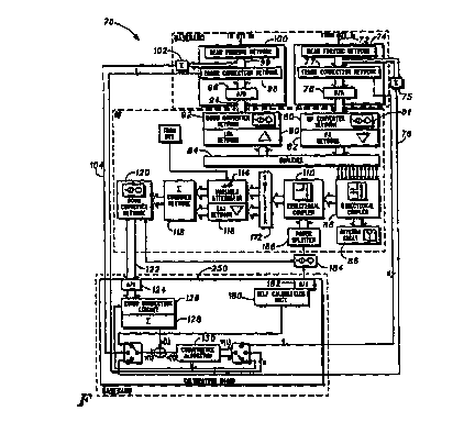
Referring now to FIG. 3, in which there is shown a detailed block diagram. of
a
transceiver ?0 having an associated calibration system according to a
preferred embodiment of the present invention. The transceiver 70 comprises
a transmitter section and a receiver section for respectively transmitting and
receiving signals. Although the following description makes specific reference
to the transceiver for use in a Base Transceiver Station (BTS), it will be
CA 02227522 1998-O1-21
WO 97/44920 PG'T/EP97/01918
_7_
understood that the present invention is not limited to use within such
infrastructure equipment, and that adaptation of the transceiver in terms of a
mobile communication unit, for example, is contemplated.
Considering the transmitter portion of the transceiver 70, the transmitter
' portion is responsible for producing a signal in a format suitable for
transmission. An encoded signal 72 (at digital baseband from a BTS) is applied
to a beam forming network 74 that applies weighting factors (coefficients)
suitable for adapting the signal for transmission. Outputs from the beam
forming network 74 are tapped for subsequent use in calibration of the
transmitter section, with each output typically combined in a first summing
unit 75 to provide a first composite signal 76 having an unique
characteristic.
Particularly, the composite signal is entirely representative of its
individual
component vectors since a summation of these components is unique.
Outputs from the beam forming network 74 are also subjected to an error
correction network 77 that modifies the weighting factors to account for
discrepancies (errors). subsequently introduced by components in the
transceiver portion (which discrepancies would, if left unchecked, adapt a
beam pattern ultimately transmitted from the transceiver 70). Furthermore,
while still at baseband, each individual error corrected, weighted coefficient
is
converted from digital to analog form in a digital-to-analog (D/A) converter
78,
which digital forms are then modulated onto a channel at an allocated Radio
Frequency (RF), e.g. 900 Megahertz (MHz), by an up-converter network 80.
As will be understood, the up-converter network 80 comprises a sufficient
number of mixers and frequency generators 81 required to modulate each
analog input received from the D/A converter 78. Subsequent to up-
conversion, a power amplifying network 82 amplifies each signal prior to each
of these signals being applied to a first duplexer 84. Outputs from the first
duplexer are applied to respective elements in an antenna array 86 (via a
first
path in a first directional coupler 88) for transmission. The first
directional
coupler 88 is usually placed immediately behind the antenna array 84 to
reduce errors in the feed network, and removes a small fraction of both a
received and transmitted signal.
With regard to the function generally performed by an error correction
network, such as error correction network 77, such a circuit principally
provides error correction for significant errors introduced by active
components, such as the up-converter network 80 and the power amplifying
CA 02227522 1998-O1-21
WO 97/44920 PCT/EP97/01918
_g_
network 82 in the transmitter (and corresponding networks in the receiver),
and to a lesser extent smaller errors introduced by passive. elements, such as
the first dupiexer 84. As will be appreciated, errors introduced by active
components result from these active components having, for example, a
temperature dependence, some form of gain variation or a performance
deviation induced by ageing of the active component.
The antenna array 86, directional coupler 88 and f~.rst duplexer 84 also form
part of the receiver section of the transceiver 70, with individual RF signals
received at each element of the antenna array 86 being routed through the
first directional coupler 88 and first duplexer 84 to a first bank of Iow
noise
amplifiers 90. Subsequent to an amplification process, each signal is down
converted to baseband in a first down-converter netv~tork 92 to provide
individual signals 94 to a first analog-to-digital (A/D) converter 96. Digital
I5 signals corresponding to those originally received by each of the elements
in
the antenna array 86 are then fed through an error correction network 98
which corrects for errors introduced into the received signals by the
components in the receive chain, with resultant error corrected received
signals 99 each being supplied to receiver circuitry of a BTS via a beam
forming network 100. The resultant error corrected received signals 99 are
also tapped prior to application to the beam forming network 100 for
subsequent use in calibration of the receiver section, with each output
typically combined in a second summing unit 102 to provide a second
composite signal 104 havi_n.g an unique characteristic.
The transceiver 70 further includes error correction and calibration
circuitry,
operative at digital baseband, for correcting errors introduced into
transmitted
and received signals by components within the transceiver 70, as previously
explained. As will be understood, in order for calibration of either the
transmit
or receive chain to occur, it is necessary to attempt to replicate an
unprocessed signal, i.e. to reproduce an uncorrupted signal that was
originally
applied to either the transmit or receive chain. As such, the transceiver 70
additional includes a second directional coupler I10 coupled to the first
directional coupler 88, with the second directional coupler 110 arranged to
4
receive signals passed through the first directional coupler 88 in both the
transmit and receive paths. In this way, signals applied to {or received from)
each element in the antenna array will also be applied to the second
directional coupler 110. It will be appreciated that the calibration process
is
CA 02227522 1998-O1-21
WO 97/44920 PCT/EP97/01918
_g_
based on a baseband beamforming system (rather than an equivalent RF
beamformer technique) because phase and amplitude signal shifts are easier
to implement at baseband.
A second duplexer 112 is coupled to the second directional coupler 110 to
route
signals to one of a bank of variable attenuators I14 or a second bank of low
noise amplifiers I16 (dependent upon whether signals are being applied to or
received from the antenna array 86). Specifically, a received signal is
amplified, while a transmitted signal is attenuated to a dynamic range
required for down conversion and conversion to digital form. Subsequent to
either attenuation or amplification, signals are typically routed through a
combiner network 118 before being down converted in frequency to a
baseband level in a second down-converter network 120.
It will be appreciated that both the first 90 and second 116 banks of low
noise
amplifiers provide identical amplification. Additionally, it will be
appreciated
that, unlike the actual receive chain which is constrained by to a specific
limited signalling bandwidth of, say, 200kHz, the error correction and
calibration circuitry is not bandwidth limited and therefore has a very much
greater bandwidth.
Ideally, a signal that has been up-converted and then immediately
down-converted (or vice versa) within the transceiver should be identical to
the original, corresponding signal (i.e. identical to either those signals
applied to
the first error correction network 77 or those obtained from the second error
correction network 98). However, if any discrepancies exist between these
signals, then these discrepancies represent errors introduced by the
respective transmit and receive chains. In conventional fashion, these errors
are corrected in pre-emptive fashion by applying vector correction factors
(weighting factors), via a feedback mechanism, in the error correction
networks 77 and 98. More explicitly, signals I22 are firstly converted to a
digital format in a second A/D converter 124 and then applied in turn through
an error correction circuit 126 (the purpose of which will be described
subsequently) and a third summing block 128. Again, the effect of the third
summing block I28 is to provide a third composite signal x(t) having an unique
characteristic that mimics the characteristics of the individual signals
originally applied to the second A/D converter 124. Then, as will be generally
understood, weighting factors for each signal branch (path) in either of the
CA 02227522 1998-O1-21
WO 97/44920 PCT/EP97/01918
-10-
error correction networks 77 and 98 (or the error correction circuit 126) may
then be determined by appropriate comparison (mapping) of the third
composite signal x(t) to the first composite signal 76 or the second composite
signal 104. A resultant signal e(t) from this comparison {mapping) is then
subjected to a suitable convergence technique in a convergence algorithm
block 130, typically implemented within a microprocessor.
There are several algorithms that may be used for the purpose of determining
the weighting factors for each path; with the simplest perhaps being the
technique known as Least Mean Square (LMS) convergence. For a system
such as GSM (with a burst duration of 0.577ms and a calibration process
which is relatively slow), the LMS algorithm is most suited. However, other
convergence algorithms, such as Fast-Kalman, can also be used. As stated,
the LMS algorithm is responsible for calculating suitable weighting factors
that compensate for phase and amplitude errors introduced by various
components in a given signal path. As will be understood, the LMS algorithm
basically compares a signal with a desired form of it, and then generates an
error based on the difference. Therefore, given a sufficient uncorrelated
observation period, the LMS algorithm calculates a set of weighting factors
for
the error correction networks of the transceiver to mitigate against the
effects
of component induced amplitude and phase variations.
As will be understood, communication systems utilising Gaussian Minimum
Shift-Keying (GMSK) require a constant communication envelope, with real-
time correction possibly prohibited by a technical standard, such as in GSM.
Therefore, in such circumstances, it would be usual to correct the next frame
of data in the communication sequence (or the next burst transmission, e.g.
the succeeding time slot). In practice, the LMS algorithm will calculate the
correction weights during the active part of burst, and only correct the
errors
during the guard times for the next active burst. Furthermore, with specific
reference to the receive chain of the transceiver 70, the requirement to
repeatedly calibrate the receive chain is diminished compared against the
requirement for calibration in the transmit chain because less power is
dissipated in the receiver chain and, as such, components are less susceptible
to temperature induced performance variation.
Unfortunately, the feedback mechanism for correcting' the amplitude and
phase errors introduced by components in both the transmit and receive
CA 02227522 1998-O1-21
WO 97/44920 PCT/EP97l01918
-11-
paths of the transceiver 70 assumes that there are no errors present in the
error correction and calibration circuitry I10-120, which assumption is in
reality flawed. Therefore, the present invention provides a calibration
mechanism for the error correction and calibration circuitry 1I0-120 itself,
which internal calibration mechanism is ostensibly transparent to any
transceiver functions. Specifically, calibration of the error correction and
calibration circuitry 110-120 is achieved by applying a pseudo-random
sequence on a broadband (spread spectrum) basis to the calibration circuitry,
and then determining whether a processing gain for the error correction and
I0 calibration circuitry has altered.
Referring firstly to FIG. 4, a plurality of channels 150-160 of fixed
bandwidth
are shown within a total system bandwidth 162 of a conventional
communication system. Turning to FIG. 5, one of these channels I54, say
channel 3, has been overlaid (for illustrative purposes) with a broadband
signal 164, according to the present invention. As can be seen, the effect of
overlaying a channel 154 with a broadband signal is to produce a ripple in the
waveform. Furthermore, as will be appreciated, the broadband signal is
available for use in a calibration process because the transceiver 70 must be
capable of receiving all channels available to the communication system.
Therefore, when considering a communication system such as GSM, the
broadband signal could potentially be anything up to 900MHz in bandwidth,
while each individual channel only having a bandwidth of 200kHz.
According to a preferred embodiment of the present invention a broadband
signal having a very low power level (below any noise threshold) and having a
very short pulse per bit is injected {superimposed) on top of an actual, real-
time, information bearing narrowband signal (for transmission from or
reception by each element in the antenna array 86 of the transceiver 70),
such that the broadband signal does not corrupt the narrowband signal.
Specifically, with reference to FIG. 3, a self calibration unit generates a
test
sequence, such as a pseudo-random number sequence (PRNS), that is
converted into analog form in a second D/A converter prior to up-link
conversion in a modulation network 184. After communication through a
power sputter 186, the now digitised and modulated PRNS is routed through
the second directional coupler 110. As such, the digitised and modulated PRNS
exhibits identical characteristic to those of a signal on a transmit or
receive
channel, ~ and the subsequent apparatus appropriately down converts and
CA 02227522 1998-O1-21
WO 97/44920 PCT/EP97/01918
-I2-
routes this digitised and modulated PRNS to the second A/D converter I24, as
previously described. Specifically, two orthogonal pseudo-random number
sequences having an appropriate chipping rate (e.g. for a GSM based system
having a 25MHz spectrum allocation for the up- and down-Iinks, a chipping '
rate of up to 80ns can be used) are quadrature modulated on the midband of
the available spectrum of the selected up-Iink or down-link. This complex
°
passband signal is then injected at a power Ievel below the noise floor of the
system into all N branches of the error correction and calibration network
110-130. Depending on the portion of the spectrum used, the complex
passband signal will take the appropriate path through either the bank of low
noise amplifiers 116 or the bank of variable attenuators 114. After passing
through the combiner network 1I8, the complex passband signal is down
converted to baseband, sampled and converted to digital form. The received
signal is then combined and correlated with spreading codes used for the I-
and
I5 Q-channels for a time appropriate to obtain sufficient processing gain for
self
calibration purposes. A correlation subsequently performed between the
original PRSN and the modulated-demodulated PRSN routed through the
second duplexer 112 determines errors in the error correction and calibration
network I10-130. In. a similar manner to that previously described, a suitable
convergence algorithm, such as LMS, is used to determine weighting factors
for the error correction and calibration network 110-130, which weighting
factors are then applied by the error correction circuit 126 during operation
thereof.
FIG. 6 illustrates, in more detail, circuitry used in FIG. 3 to overlay a
broadband signal on a channel, as required in FIG. 5. In the specific instance
of
s
the preferred embodiment, the self calibration unit 180 is arranged to provide
quadrature I- and Q-channels having a 90° phase Iag relationship. I-
channel
component 200 and Q-channel component 202 are respectively encoded with
by separate pseudo-random number sequences (PRNSI and PRNSQ) 204 and
206 in combining networks 208 and 210. Subsequently, the I-channel and the
Q-channel are both modulated with a broadband signal (cosco~t and sinc~~t) in
combining networks 212 and 214, respectively, before being summed together
in summing network 216 to produce a composite test signal. The composite
test signal produced by summing network 216 is representative of a channel
218, which composite test signal is then injected into the second directional
coupler 110, as previously described. After splitting the composite test
signal
218 into respective I (222) and Q (224) signal components in signal splitter
CA 02227522 1998-O1-21
WO 97/44920 PCT/EP97/01918
-13-
220, down conversion of the I and Q signal components is achieved by
hardwiring the broadband signal (cosco~t and sinw~t} into mixing networks 226
and 228 in an attempt to regenerate the pseudo random number sequences
{for the I and Q channels), although it is likely that the regenerated
sequences
contain amplitude and phase variations l and q, respectively.
Therefore, bearing in mind that respective bits of the pseudo random
broadband signal (i.e. the composite test signal) are transmitted at very low
{sub-noise) power levels e.g. -140dBm, and providing that a common local
oscillator is used to modulate (up convert) and demodulate (down convert) the
I and Q channel components for use in the error correction and calibration
network 110-130, then any errors introduced into the injected pseudo random
number sequences result from amplitude and phase errors introduced by the
second duplexer 110, the bank of variable attenuators 114, the second bank of
low noise amplifiers 116 and combiner network 118. Therefore, as will be
understood, by multiplying together respective bits of the originally injected
pseudo-random number sequences with the regenerated pseudo random
number sequences, and then summing together for each I and Q channel
component, a processing gain PG (derived from the length of the original
PRSN) 230 and 231 can be determined for each channel in the error correction
and calibration network 110-130. In the event that the processing gain 230
and 231 for either quadrature channel falls below a predete~~ned threshold,
as illustrated by the graphical representation, a revision of weighting
factors
applied by error correction circuit 126 is required to appropriately
compensate
for any amplitude and phase variations.
FIG. 7 illustrates an I-channel and Q-channel error displacement introduced
by conventional transceiver equipment and the error correction and
calibration network 110-130. Therefore, since amplitude OA can be
determined from a peak value of the processor gain, a phase variation ~~ can
be determined by the LMS conversion algorithm (or the like), and suitable
weighting factors {correction vectors} for the error correction circuit 126
determined. Consequently, since the error correction and calibration circuitry
is independently calibrated to produce ostensibly zero errors, any weighting
factors (vectors) applied to a signal by the error correction networks 77 and
98 for amplitude and phase correction must be correct. It is however noted
that only a single mixer is uncalibrated and remains outside the
self calibration path, albeit that this mixer only has a few degrees of phase
CA 02227522 1998-O1-21
WO 97/44920 PCT/EP97/01918
-14-
variation (over a wide ambient temperature range) and is subject to very low
signal power levels.
As will be appreciated, the convergence algorithm and processing gain are
typically implemented within a microprocessor (or the like). Indeed, the
majority of functions performed within the calibration board of FIG. 3,
generally identified by reference numeral 250, are performed within a
microprocessor.
Additionally, as the weighting factors are an indication of how each path in
the
transceiver is behaving in terms of amplitude and phase, the present
invention is capable of being able to identify faulty branches of the antenna
array 86. This may be achieved by a simple comparison between the
calculated weighting factors for each path and acceptable correction factors
for the amplitude and phase variations in these paths. Furthermore, although
the preferred embodiment of the present invention discusses the use of only
one convergence algorithm, it is possible to use a separate convergence loop
for the self calibration of the error correction and calibration network to
provide a simultaneous calibration process. In additional, it would also be
possible to use separate down converters for the receiver and transmitter
paths in order to facilitate concurrent calibration processes for these
separate
communication functions.
It will, of course, be understood that the above description has been given by
way of example only and that moclifications in detail, such as the utilisation
of
common circuit components between the receiver chain and the error
correction and calibration network 110-130 to reduce component count, may
be made within the scope of the invention. Clearly, the technique of the
present invention for calibrating a calibration network using an overlaid
broadband pseudo-random signal is applicable to transmitters and receiver
circuitry used in isolation, although it has been described specifically in
relation only to a transceiver for the purpose of brevity. Also, while the ,
present invention may utilise the entire system bandwidth (spectrum)
available to the communication device in generating the broadband signal, it
will be appreciated that the broadband signal need only be relatively broad
compared to the narrowband channels and that a proportion of the entire
system bandwidth could therefore be used.