Note: Descriptions are shown in the official language in which they were submitted.
CA 0222806~ 1998-01-27
W O 97/05505 PCT/CA95/00457
F ~AT P2~NEL D~ ~ OK FOR }~aDIATIO N I~C~GI N~
WITH REDUCED ELEC~RONIC NOIQE
-~nNlC~L FIELD
The present invention relates to imaging
systems and in particular to a flat panel detector for
radiation imaging.
BACKGROUND ART
X-ray imaging systems are widely used in
medical diagnosis and industrial and security inspection
environments. One well known prior art x-ray imaging
system is commonly referred to as an x-ray image
intensifier ("XII") system. The XII system includes a
large image tube that converts a low intensity x-ray
image into a visible image. Incident x-rays are
transmitted through a low absorbing window, then absorbed
by an input phosphor screen and converted into a light
image. On the inner surface of the input phosphor screen
is a photocathode which converts the light into
photoelectrons. The photoelectrons are accelerated and
focused by an electrical static lens. The focused
photoelectrons bombard an output phosphor screen and are
converted into an optical image. A charge-coupled device
("CCD") or a camera tube is coupled to the output
phosphor screen to convert the light image into an
electronic video signal.
However, the XII system suffers from a number
of problems due to the multiple conversion stages,
resulting in a reduction in image resolution and image
contrast as well as pincussion distortion caused by the
magnification error of the electrical static lens.
Moreover, the XII system is complex and bulky.
CA 0222806~ 1998-01-27
W O 97/05505 PCT/CA95/004S7
To overcome the problems associated with the
XII system, alternative x-ray imaging systems employing
flat-panel radiation image sensors have been proposed.
For example, U.S. Patent No. 4,382,187 to Fraleux et al.
and U.S. Patent No. 4,689,487 to Nishiki et al. disclose
early designs of large area flat-panel radiation image
sensors for use in radiation imaging systems. These
flat-panel sensors are responsive to incident x-rays and
generate output signals representative of a radiation
image.
U.S. Patent No. 5,079,426 to Antonuk et al.
discloses a direct-detection x-ray image sensor
incorporating an amorphous silicon thin film transistor
("TFT") switch and photodiode array. X-rays are detected
by a phosphor screen that is placed on the top of the TFT
switch and photodiode array. When x-rays interact with
the phosphor film, light photons are generated and
converted into electronic charges by the photodiode
array. The charges are read out via the TFT switches to
generate an image. However, problems exist with this
sensor. Because the sensor employs a phosphor screen to
detect the x-rays, blurring occurs due to the fact that
the light photons are emitted in all directions and are
scattered inside the phosphor screen. This results in a
poor image resolution. Although higher resolution can be
obtained by increasing the thickness of the phosphor
film, this is done at the expense of signal gain.
In an article entitled "New solid-state image
pickup devices using photosensitive chalcogenide glass
film," by T. Tsukada et al., published in the Proc~e~;ngs
of IEEE International Electron Devices Meeting, 1979,
pp.l34-136, a solid state image sensor is disclosed
including a photoconductive selenium film deposited on a
n-chAn~el MOSFET switch array made from crystalline
silicon. Although this image sensor is suitable for some
CA 0222806~ 1998-01-27
W O 97/05505 PCT/CA9~/00457
imaging applications, it is not suited for large area
radiation imaging applications due to the difficulties in
fabricating a large sensor array on a crystalline silicon
wafer.
In an article entitled "Digital radiology using
self-scanned readout of amorphous selenium," authored by
W. Zhao et al. presented at COMP91, Canadian Organization
of Medical Physicists, Winnipeg, Manitoba, Canada, June
19, 1991, a flat-panel x-ray image sensor is disclosed.
The image sensor includes a thick amorphous selenium film
(a-Se) on a two-~ nRional TFT switch array. The TFT
switches are arranged in rows and columns to form a two-
~;me~ional imaging system. Gate lines interconnect the
15 TFT switches in each row while source lines interconnect
the TFT switches in each column. The thick selenium film
is deposited directly on top of the TFT switch array and
a top electrode is deposited on the selenium film. When
x-rays are incident on the selenium film and the top
electrode is biased with a high voltage, electron-hole
pairs are separated by the electric field across the
thickness of the selenium film. The holes which are
driven by the electric field move toward the pixel
electrodes (i.e. the drain electrodes of the TFT
switches) and accumulate. This results in a charge being
held by the pixel electrodes which can be used to develop
an x-ray image. The charge held by the pixel electrodes
can be read by supplying a pulse to each gate line. When
a gate line receives a pulse, the TFT switches in the row
turn on, allowing the signal charges on the pixel
electrodes to flow to the source lines. Charge
amplifiers connected to the source lines sense the charge
and provide output voltage signals proportional to the
charge and hence, proportional to the radiation exposure
on the selenium film.
CA 0222806~ 1998-01-27
W O 97/05505 PCT/CA95/00457
Because a thick amorphous selenium film is
deposited on the TFT switch array, a few problems may
arise which reduce image quality. During x-ray exposure,
most of the holes are drawn to the pixel electrodes by
the applied electric field, but some of them are drawn to
the dielectric film which overlies the source and gate
lines. As this occurs, the electric field above the
dielectric film decreases. Because the ~uantum
efficiency of an a-Se film is approximately
approportional to the electric field in the bulk of the
a-Se film, signal charges generated by x-ray exposure of
the a-Se film decline. Once the electric field decreases
to a certain level, x-ray generated holes become trapped
in the bulk of the selenium film above the dielectric
film. Also, the trapped holes in the bulk of the selenium
film may be released slowly by thermal energy and
collected by adjacent pixel electrodes, resulting in
decay-lag which again affects image ~uality.
U.S. Patent No. 5,319,206 to Lee discloses a
flat panel image sensor similar to that described by Zhao
except that a dielectric film is placed between the x-ray
conversion layer and the pixel electrodes or between the
x-ray conversion layer and the top electrode. Because no
DC current component flows from the top electrode to the
pixel electrode through the x-ray conversion layer due to
the dielectric film, the charge stored by the pixel
electrode must be read using a capacitive coupling
method. Also, the reset operation (i.e. the removal of
residual charges in the x-ray conversion layer) must be
carried out by inverting the polarity of the biasing
voltage applied to the top electrode. Although this
image sensor has a high voltage tolerance due to the fact
that the pixel electrodes pick up a differential voltage
proportional to the radiation exposure (and not a DC
component of the voltage applied to the top electrode),
the image sensor suffers drawbacks. Specifically, the
CA 0222806~ 1998-01-27
W O 97/05505 PCT/CA95/00457
image sensor is difficult to operate in real time and
requires a complicated driving scheme.
~ European Patent No. 0,588,397 discloses an x-
ray imaging device designed to deal with the above
described problems. The x-ray imaging device includes a
doped semiconductor layer covering all of the TFT switch
array with the exception of the pixel electrodes. The
doped semiconductor film allows holes collected in the
semiconductor film above the source and gate lines (i.e.
the area between adjacent pixel electrodes) to drift
towards the pixel electrodes. However, one problem
exists in that since the semiconductor layer overlays the
entire area of the TFT switch array between the pixel
electrodes, a diffusion of charges from one pixel area to
adjacent pixel areas may occur especially around bright
image locations. This results in a reduction in image
resolution.
In addition to the drawbacks noted above with
respect to the prior art image sensors, the above
described flat panel image sensors suffer from problems
due to electronic noise. Because the image sensors
include an MxN matrix of TFT switches, there are MxN
intersections between the gate lines driving the TFT
switches and the source lines upon which stored charges
are to be sensed. Fluctuations in the potential on the
gate lines become coupled to the source lines through
parasitic capacitance at overlapping nodes of the gate
and source lines and through parasitic capacitance at the
TFT switches. The parasitic capacitance at the TFT
switches is a result of feed-through charges generated by
switching the TFT switches on and off. In both cases,
this parasitic capacitance is fed to the source lines
where it is passed to output circuitry in the form of
electronic noise. This results in a reduction in image
CA 0222806~ 1998-01-27
W O 97/05505 PCT/CA95/00457
resolution. Accordingly, there exists a need for an
improved flat panel detector for radiation imaging.
It is therefore an object of the present
invention to provide a novel flat panel detector for a
radiation imaging system which obviates or mitigates at
least one of the above-mentioned problems.
~I8CLO8URE OF THE lwv~lON
According to one aspect of the present
invention there is provided a flat panel detector for
radiation imaging comprising:
an array of pixels arranged in rows and
columns, each of said pixels including a pixel electrode
to store a charge proportional to the exposure of said
pixel to radiation;
a radiation transducer over said array to be
exposed to incident radiation;
a plurality of source lines, each
interconnecting the pixels of individuals ones of one of
the rows or columns of said array;
a plurality of gate lines, each interconnecting
the pixels of individual ones of the other of the rows or
columns of said array, said source and gate lines
crossing one another to define a plurality of overlapping
nodes; and
shielding means to shield said gate lines from
said source lines at said overlapping nodes to reduce
parasitic capacitance at the overlapping nodes.
According to another aspect of the present
invention there is provided a flat panel detector for
radiation imaging comprising:
a radiation transducer including a radiation
conversion layer and an electrode on one side of said
radiation conversion layer;
CA 0222806~ 1998-01-27
W O 97/05505 PCT/CA95/00457
an array of pixels arranged in rows and columns
on the other side of said radiation conversion layer,
each of said pixels including a pixel electrode to
ac- Il ate charge as a result of hole drift in said
radiation conversion layer occurring upon exposure of
said radiation transducer to radiation and when said
electrode is biased;
a plurality of source lines upon which charges
accumulated by said pixels can be sensed, each of said
source lines connecting the pixels of individual ones of
one of said rows or columns;
a plurality of gate lines upon which gating
signals are supplied to allow accumulated charges to be
sensed, each of said gate lines connecting the pixels of~5 individual ones of the other of said rows or columns; and
shielding means to shield said gate lines from
said source lines at overlapping points thereof to reduce
parasitic capacitance at said overlapping points.
According to still yet another aspect of the
present invention there is provided in a method of
forming a flat panel detector for radiation imaging
including a radiation transducer having a radiation
conversion layer and an electrode on one side thereof and
an array of pixels arranged in rows and columns on the
other side of said radiation conversion layer, each pixel
including a pixel electrode to store charge proportional
to the exposure of said flat panel detector to radiation,
each pixel in individual ones of one of the rows or
columns of the array being interconnected by a source
line and each pixel in individual ones of the other of
the rows or columns being interconnected by a gate line,
wherein said method further comprising the step of:
shielding the gate lines from the source lines
at overlapping points thereof to reduce parasitic
capacitance at said overlapping points.
CA 0222806~ 1998-01-27
W O 97/05S05 PCT/CA95/00457
In one embodiment, the shielding means is in
the form of a biased metal shielding plate disposed
between the gate and source lines adjacent the
overlapping nodes. In another embodiment, the shielding
means is in the form of a shielding pad formed of
semiconductor material disposed between the gate and
source lines adjacent the overlapping nodes and connected
to a biased metal conductor.
Preferably, the pixels are constituted by thin
film transistors. In one embodiment, each of the thin
film transistors includes a drain electrode constituting
a pixel electrode, a source electrode constituting a
portion of a source line and at least one top gate
electrode disposed between the source and drain
electrodes. The source, drain and at least one top gate
electrodes are disposed above a channel and are laterally
offset from the gate line. The at least one top gate
electrode is also electrically connected to the gate line
at a location spaced from the channel. In another
embodiment, the at least one top gate electrode is
constituted by a pair of narrow, laterally spaced top
gate electrodes, both of which are electrically connected
to the gate line at a location spaced from the channel.
The present invention provides advantages in
that since the gate and source lines are shielded at
their overlapping nodes, parasitic capacitance at the
overlapping nodes is reduced. In addition, when the
pixels in the flat panel detector include at least one
top gate electrode that is laterally offset from the gate
line, parasitic capacitance is further reduced.
CA 0222806~ 1998-01-27
WO 97/05505 PCT/CA95/00457
~RIEF DESCRIPTION OF THE DR~WING8
Embodiments of the present invention will now
be described more fully with reference to the
accompanying drawings in which:
Figure 1 is a schematic of a flat panel
detector for radiation imaging in accordance with the
present invention;
Figure 2 is an equivalent circuit of a pixel
forming part of the flat panel detector illustrated in
Figure 1;
Figure 3 is a top plan view of a portion of the
flat panel detector of Figure l;
Figure 4 is a cross-sectional view of Figure 3
taken along line 4-4 showing a pixel;
Figure 5 is a plot of some characteristics of
the pixel of Figure 4;
Figure 6 is a cross-sectional view of an
alternative embodiment of a pixel forming part of a flat
panel detector for radiation imaging in accordance with
the present invention;
Figures 7a to 7d are schematic illustrations of
characteristics of a prior art TFT switch and a TFT
switch in accordance with the present invention;
Figure 8 is a top plan view of a portion of yet
another embodiment of a flat panel detector for radiation
imaging in accordance with the present invention; and
Figure 9 is a cross-sectional view of Figure 8
taken along line 9-9.
BE8T MODES FOR CARRYING OUT THE lNV~'~. lON
Referring now to Figure 1, a flat panel
detector for radiation imaging is shown and is generally
indicated by reference numeral 20. The flat panel
detector includes a plurality of pixels 22 arranged in
rows and columns. Gate lines 24 interconnect the pixels
CA 0222806~ 1998-01-27
W O 97/05SO5 PCT/CA95/00457
22 of each row while source lines 26 interconnect the
pixels 22 of each column. The gate lines 24 lead to a
gate driver circuit 28 which provides pulses to the gate
lines in succession in response to input from a control
circuit 29. The source lines 26 lead to charge
amplifiers 30 which in turn are connected to an analog
multiplexer 32. The analog multiplexer provides image
output which can be digitized to create a digitized
radiation image in response to input from the control
circuit 29.
Figure 2 shows an equivalent circuit of one of
the pixels 22. As can be seen, the pixel includes a
radiation transducer CSE coupled to a storage capacitor C
in the form of a pixel electrode 36. The pixel electrode
36 constitutes the drain electrode of a thin film
transistor ("TFT") switch 38. The source electrode of
TFT switch 38 is coupled to one of the source lines 26
while the gate electrode of the TFT switch 38 is coupled
to one of the gate lines 24.
When the radiation transducer CSE is biased and
is exposed to radiation, it causes the pixel electrode 36
to store a charge proportional to the exposure of the
radiation transducer CSE to radiation. Once charged, the
charge can be read by supplying a gating pulse to the
gate terminal of TFT switch 38. When the TFT switch
receives the gate pulse, it connects the pixel electrode
36 to the source line 26 allowing the pixel electrode to
discharge. The charge on the source line 26 is detected
by the charge amplifier 30 which in turn generates an
output voltage proportional to the detected charge. The
output voltage of the charge amplifier 30 is conveyed to
the analog multiplexer 32.
The design of the flat panel detector 20 is
such to obviate or mitigate at least some of the
CA 0222806~ 1998-01-27
WO 97/05505 PCT/CA95/00457
11
disadvantages associated with the prior art designs
discussed previously by reducing parasitic capacitance in
the flat panel detector and thereby reducing electronic
- noise.
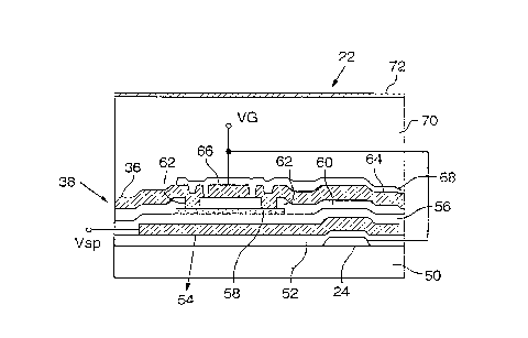
Referring now to Figures 3 and 4, a portion of
the array of pixels 22 formed in accordance with the
present invention is shown. The pixels 22 including the
gate and source lines 24 and 26 are fabricated on a
common glass substrate 50. Figure 4 best illustrates one
of the pixels. As can be seen, the gate line 24
associated with the pixel 22 is deposited on the
substrate 50. A gate insulating layer 52 formed of sio2
or SiNX overlies the substrate 50 and the gate lines 24.
Deposited on the gate insulating layer 52 above
the gate line 24 is a shielding plate 54 formed of metal
and coupled to a DC potential voltage source Vsp. A
dielectric film 56 formed of SiO2, a-SiN or Al2O3 overlies
the shielding plate 54 and the portions of the gate
insulating layer 52 not covered by the shielding plate.
A semiconductor material layer formed of Cadmium Selenide
(CdSe) defines the channel 58 of the TFT switch 38 and is
deposited on the dielectric film 56. The channel 58 is
disposed over the shielding plate 54 and is laterally
offset from the gate line 24 by a distance of
approximately 1 to lO~m.
A passivation layer 60 in the form of an SiO2
layer overlies the dielectric film 56 and the channel 58.
Vias 62 are provided in the passivation layer 60 to
expose portions of the channel 58. Contacting the
~h~nnel 58 through one of the vias 62 and disposed over
the passivation layer 60 is the pixel electrode 36 which
defines the drain electrode of the TFT switch 38. A
source electrode 64 also~contacts the channel 58 through
the other of the vias 62 and is disposed over the
CA 0222806~ 1998-01-27
W O 97/05505 PCT/CA95tOO457
12
passivation layer 60. A top gate electrode 66 is
deposited on the passivation layer 60 between the pixel
and source electrodes 38 and 64 respectively. The top
gate electrode 66 is spaced from the source and pixel
electrodes by gaps in the order of a few microns. The
top gate electrode 66 is electrically connected to the
gate line 24 through vias 80 formed in the TFT array
structure and through an aperture 82 formed in the
shielding plate 54 (see Figure 3). A top passivation
layer 68 in the form of a photoresist overlies the TFT
switch 38 except in the area over the pixel electrode 36.
Although only one TFT switch 38 has been described, it
should be apparent to those of skill in the art that each
TFT switch 38 in the array has a similar structure and
that each TFT switch 38 is formed on the substrate 50 at
the same time.
The shielding plate 54 also has apertures 84
provided in it that are aligned with the gate and source
lines 24 and 26 respectively. The apertures 84 are
positioned at regions of the TFT switch array where the
gate and source lines do not overlap.
Above the TFT switch array is the radiation
transducer CSE. The radiation transducer is in the form
of a selenium (Se) radiation conversion layer 70 having
a thickness of approximately 300~m to 500~m. Above the
radiation conversion layer is a top electrode 72 formed
of In, Al or Au. The top electrode 72 is coupled to a
high potential voltage source 74 in the order of 3kV to
provide the necessary bias to the radiation transducer
SE-
In operation, the top electrode 72 is biased by
the high potential voltage source 74 and the flat panel
detector 20 is exposed to radiation, resulting in an
electric field being created in the radiation conversion
- CA 0222806~ 1998-01-27
W O 97/05505 PCT/C A95/00457
13
layer 70 which causes electrons to move toward the top
electrode 72 and holes to move towards the pixel
electrodes 36. The majority of the holes migrate to the
exposed pixel electrodes where positive charges are
accumulated. The charges accumulated by the pixel
electrodes are proportional to the exposure of the pixels
22 to radiation.
After the flat panel detector 20 has been
exposed to radiation and it is desired to create a
radiation image, a DC voltage is applied to the shielding
plate 54. The control circuit 29 is then caused to
trigger the gate driver 28 to supply a switching pulse to
each gate line 24 in succession. When a switching pulse
is applied to a gate line 24, the switching pulse is also
applied to the top gate electrode 66 of each TFT switch
38 connected to that gate line. By manipulating the DC
voltage on the shielding plate 54 and the on/off voltage
of the switching pulse supplied to the gate line, and
hence the top gate electrode, a high on/off current ratio
for the TFT switches 38 can be obtained. Figure 5 shows
the drain current verses the top gate electrode voltage
characteristics of the TFT switches 38 for various DC
voltages applied to the shielding plate 54.
This design of the TFT switches 38 provides
advantages in that because there is no overlap between
the top gate electrodes 66, which drive the channels 58,
and the source and drain electrodes, parasitic
capacitance in the TFT switches is reduced significantly.
Also, because the source lines 26 are shielded from the
gate lines 24 by the shielding plate 54, electronic noise
appearing on the source lines due to potentials placed on
the gate lines is reduced. This is due to the fact that
because the shielding plate 54 is connected to a DC
voltage source Vsp, electronic noise resulting from the
CA 0222806~ 1998-01-27
W O 97/05505 PCT/CA95/00457
14
switching pulses applied to the gate lines 24 is shunted
to ground.
In order to reduce load capacitance on the gate
lines 24, the apertures 84 are provided in the shielding
plate 54. By reducing load capacitance in this manner,
electronic noise in the flat panel detector 20 is further
reduced.
Referring now to Figures 6 and 7a to 7d, an
alternative embodiment of a flat panel detector for
radiation imaging is shown. In this embodiment like
reference numerals will be used to indicate like
components with a "100" added for clarity. The pixels
122 and the flat panel detector 120 are very similar to
those shown in the previous embodiment except that two
spaced top gate electrodes 166a and 166b are disposed on
the passivation layer 160 between the pixel and source
electrodes 136 and 164 respectively. The two top gate
electrodes 166a and 166b are electrically connected to
the gate line 124.
The operation of the flat panel detector 120 is
virtually identical to that of the previous embodiment
except that the two top gate electrodes 166a and 166b
reduce parasitic capacitance of the TFT switches 138 in
the form of feed-through charge coming from or into the
channels 158 as will now be described.
Figure 7a and 7b schematically demonstrate the
mechAni~ of feed-through charge occurring when a
conventional TFT switch is turned off. The feed-through
charge is proportional to the area of the driving gate
electrode. In principle, the feed-through charge can be
reduced by using a narrow gate electrode. However, by
narrowing the gate electrode, the effective length of the
potential barrier LB in the off-state is not equal to the
CA 0222806~ 1998-01-27
W 097/05505 PCT/CA95/00457
length of the channel. This results in an increase in
off-state current and a decrease in the on/off current
ratio of the TFT switch.
The use of the two top gate electrodes 166a and
166b deals with the above problem by reducing feed-
through charge. Figures 7c and 7d show the mec-h~ ~ of
feed-through charge occurring in the TFT switch 138. A S
can be seen, by using the two top gate electrodes 166a
and 166b, the effective length of the potential barrier LB
is equal to the length between the outer sides of the two
top gate electrodes (i.e. the length of the top gate
electrode shown in the previous embodiment). In
addition, the effective area of the driving top gate
electrodes is reduced. Since the length of the potential
barrier is maintained, the on/off current ratio of the
TFT ~;witch 138 remains relatively high even though feed-
through charge is reduced.
Referring now to Figures 8 and 9, yet another
embodiment of a flat panel detector for radiation imaging
is shown. In this embodiment, like reference numerals
will be used to indicate like components with a "200"
added for clarity. The flat panel detector 220 iS
designed to reduce parasitic capacitance at the
overlapping nodes of the gate and source lines 224 and
226 respectively.
The flat panel detector 220 includes an array
of pixels 222, each of which includes a TFT switch 238.
Figure 9 shows one of the TFT switches and as can be
seen, unlike the previous embodiments, the TFT switch 238
does not include a top gate electrode. Instead, the gate
line 224 beneath the channel 258 iS not shielded by a
shielding plate and therefore, is used to drive the TFT
switch. However, shielding pads 275 in the form of
semiconductor films are positioned between the gate
CA 0222806~ 1998-01-27
W 097/05505 PCT/CA95/00457
16
insulating layer 252 and the passivation layer 260 at the
overlapping nodes of the gate and source lines 224 and
226 respectively. The shielding pads are connected to a
metal strip 277 through vias 279 formed in the TFT array
structure. The metal strips are connected to a DC
potential voltage source.
During exposure of the flat panel detector 222
to radiation, the flat panel detector operates in a
conventional manner. Once exposure has been completed,
and it is desired to generate a radiation image, a
positive switching pulse is applied to the gate lines 224
in succession by the gate driver 28. When a switching
pulse is applied to a gate line 224, the potential of the
shielding pads 275 above that gate line increase. When
the potentials of the shielding pads 275 exceed a
threshold voltage, an electron charge pours into the
shielding pads from the metal strip 277 thereby creating
a charge sheet on the shielding pads 275. The charge
sheet is modulated by any potential charge on the gate
line 224. Once a charge sheet is created, no charge from
the gate line 224 can be fed through to the source line
226 above the shielding pads. By manipulating the
voltage on the metal strips 277, the threshold voltage
can be reduced to a small value thereby increasing the
shielding between the gate and source lines at the
overlapping nodes.
When the gate lines 224 are at a low potential,
the shielding pads 275 act as a dielectric film. As one
of skill in the art will appreciate, the use of the
semiconductor film shielding pads to shield the gate and
source lines at the overlapping nodes reduces parasitic
capacitance at the nodes to a greater extent than does
the shielding plate of the first embodiment.
-
CA 02228065 1998-01-27
W O 97/05505 PCT/CA95/00457
17
Although the shielding pads 275 are shown
connected to the metal strips 277 through one via 279,
multiple connections at opposed ends of the shielding
pads can be made to increase time response.
s
In addition, those of skill in the art will
also appreciate that alternative structures to reduce
parasitic capacitance in a flat panel detector are well
within the scope of the present invention as defined by
the appended claims.
-