Some of the information on this Web page has been provided by external sources. The Government of Canada is not responsible for the accuracy, reliability or currency of the information supplied by external sources. Users wishing to rely upon this information should consult directly with the source of the information. Content provided by external sources is not subject to official languages, privacy and accessibility requirements.
Any discrepancies in the text and image of the Claims and Abstract are due to differing posting times. Text of the Claims and Abstract are posted:
| (12) Patent: | (11) CA 2228243 |
|---|---|
| (54) English Title: | A SINGLE-EDGE ADJUSTABLE DELAY CIRCUIT |
| (54) French Title: | CIRCUIT A RETARD REGLABLE DE FLANC UNIQUE DE SIGNAL |
| Status: | Expired and beyond the Period of Reversal |
| (51) International Patent Classification (IPC): |
|
|---|---|
| (72) Inventors : |
|
| (73) Owners : |
|
| (71) Applicants : |
|
| (74) Agent: | BORDEN LADNER GERVAIS LLP |
| (74) Associate agent: | |
| (45) Issued: | 2008-01-08 |
| (22) Filed Date: | 1998-01-30 |
| (41) Open to Public Inspection: | 1999-07-30 |
| Examination requested: | 2002-12-20 |
| Availability of licence: | N/A |
| Dedicated to the Public: | N/A |
| (25) Language of filing: | English |
| Patent Cooperation Treaty (PCT): | No |
|---|
| (30) Application Priority Data: | None |
|---|
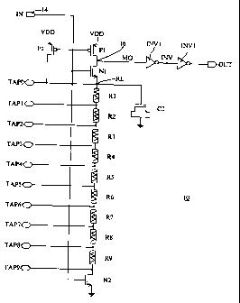
In accordance with this invention there is provided a circuit for delaying a
selected edge of an input signal for use in a deep sub-micron process
semiconductor
device, the circuit comprising an inverter element having an input and output
node, a load
element comprising resistive and capacitive (RC) elements a first transistor
element,
coupled to the RC load element and selectively operable to couple the RC
element to the
output node upon receipt of the selected edge of the input signal and for
decoupling the
RC element from the output node upon receipt of an opposite edge of the input
signal,
whereby a delay is introduced by the load element on the selected edge of the
input signal
with little negative effect on the opposite edge of the input signal.
Note: Claims are shown in the official language in which they were submitted.
Note: Descriptions are shown in the official language in which they were submitted.
2024-08-01:As part of the Next Generation Patents (NGP) transition, the Canadian Patents Database (CPD) now contains a more detailed Event History, which replicates the Event Log of our new back-office solution.
Please note that "Inactive:" events refers to events no longer in use in our new back-office solution.
For a clearer understanding of the status of the application/patent presented on this page, the site Disclaimer , as well as the definitions for Patent , Event History , Maintenance Fee and Payment History should be consulted.
| Description | Date |
|---|---|
| Inactive: IPC deactivated | 2014-05-17 |
| Inactive: First IPC from PCS | 2014-02-01 |
| Inactive: IPC from PCS | 2014-02-01 |
| Inactive: IPC expired | 2014-01-01 |
| Inactive: IPC assigned | 2013-10-31 |
| Inactive: IPC removed | 2013-10-31 |
| Inactive: IPC removed | 2013-10-31 |
| Inactive: IPC removed | 2013-10-31 |
| Inactive: First IPC assigned | 2013-10-31 |
| Time Limit for Reversal Expired | 2010-02-01 |
| Letter Sent | 2009-05-11 |
| Inactive: Office letter | 2009-05-11 |
| Letter Sent | 2009-05-05 |
| Inactive: Multiple transfers | 2009-03-20 |
| Inactive: Correspondence - Transfer | 2009-03-04 |
| Letter Sent | 2009-01-30 |
| Letter Sent | 2008-08-18 |
| Inactive: Late MF processed | 2008-03-20 |
| Letter Sent | 2008-01-30 |
| Grant by Issuance | 2008-01-08 |
| Inactive: Cover page published | 2008-01-07 |
| Pre-grant | 2007-10-09 |
| Inactive: Final fee received | 2007-10-09 |
| Notice of Allowance is Issued | 2007-04-19 |
| Letter Sent | 2007-04-19 |
| Notice of Allowance is Issued | 2007-04-19 |
| Inactive: Approved for allowance (AFA) | 2007-03-30 |
| Amendment Received - Voluntary Amendment | 2006-05-30 |
| Revocation of Agent Requirements Determined Compliant | 2006-05-12 |
| Inactive: Office letter | 2006-05-12 |
| Inactive: Office letter | 2006-05-12 |
| Appointment of Agent Requirements Determined Compliant | 2006-05-12 |
| Appointment of Agent Request | 2006-04-21 |
| Revocation of Agent Request | 2006-04-21 |
| Inactive: IPC from MCD | 2006-03-12 |
| Inactive: IPC from MCD | 2006-03-12 |
| Inactive: S.30(2) Rules - Examiner requisition | 2005-11-30 |
| Appointment of Agent Requirements Determined Compliant | 2003-03-18 |
| Inactive: Office letter | 2003-03-18 |
| Inactive: Office letter | 2003-03-18 |
| Revocation of Agent Requirements Determined Compliant | 2003-03-18 |
| Revocation of Agent Request | 2003-03-04 |
| Appointment of Agent Request | 2003-03-04 |
| Appointment of Agent Request | 2003-02-26 |
| Revocation of Agent Request | 2003-02-26 |
| Letter Sent | 2003-01-31 |
| All Requirements for Examination Determined Compliant | 2002-12-20 |
| Request for Examination Requirements Determined Compliant | 2002-12-20 |
| Request for Examination Received | 2002-12-20 |
| Inactive: Office letter | 2000-09-25 |
| Inactive: Office letter | 2000-09-25 |
| Revocation of Agent Requirements Determined Compliant | 2000-09-25 |
| Appointment of Agent Requirements Determined Compliant | 2000-09-25 |
| Revocation of Agent Request | 2000-06-08 |
| Appointment of Agent Request | 2000-06-08 |
| Revocation of Agent Request | 2000-06-07 |
| Appointment of Agent Request | 2000-06-07 |
| Inactive: Inventor deleted | 2000-05-12 |
| Inactive: Cover page published | 1999-08-03 |
| Application Published (Open to Public Inspection) | 1999-07-30 |
| Inactive: Correspondence - Formalities | 1999-04-30 |
| Inactive: IPC assigned | 1998-05-22 |
| Classification Modified | 1998-05-22 |
| Inactive: First IPC assigned | 1998-05-22 |
| Inactive: Single transfer | 1998-05-04 |
| Filing Requirements Determined Compliant | 1998-04-23 |
| Inactive: Filing certificate - No RFE (English) | 1998-04-23 |
| Application Received - Regular National | 1998-04-22 |
There is no abandonment history.
The last payment was received on 2007-01-29
Note : If the full payment has not been received on or before the date indicated, a further fee may be required which may be one of the following
Please refer to the CIPO Patent Fees web page to see all current fee amounts.
| Fee Type | Anniversary Year | Due Date | Paid Date |
|---|---|---|---|
| Application fee - standard | 1998-01-30 | ||
| Registration of a document | 1998-05-04 | ||
| MF (application, 2nd anniv.) - standard | 02 | 2000-01-31 | 2000-01-31 |
| MF (application, 3rd anniv.) - standard | 03 | 2001-01-30 | 2001-01-16 |
| MF (application, 4th anniv.) - standard | 04 | 2002-01-30 | 2002-01-25 |
| MF (application, 5th anniv.) - standard | 05 | 2003-01-30 | 2002-12-20 |
| Request for examination - standard | 2002-12-20 | ||
| MF (application, 6th anniv.) - standard | 06 | 2004-01-30 | 2003-12-19 |
| MF (application, 7th anniv.) - standard | 07 | 2005-01-31 | 2004-12-29 |
| MF (application, 8th anniv.) - standard | 08 | 2006-01-30 | 2005-12-13 |
| MF (application, 9th anniv.) - standard | 09 | 2007-01-30 | 2007-01-29 |
| Final fee - standard | 2007-10-09 | ||
| Reversal of deemed expiry | 2008-01-30 | 2008-03-20 | |
| MF (patent, 10th anniv.) - standard | 2008-01-30 | 2008-03-20 | |
| Registration of a document | 2008-06-04 | ||
| Registration of a document | 2008-10-20 | ||
| Registration of a document | 2009-03-20 |
Note: Records showing the ownership history in alphabetical order.
| Current Owners on Record |
|---|
| TRACESTEP HOLDINGS, LLC |
| Past Owners on Record |
|---|
| JODY DEFAZIO |

