Note: Descriptions are shown in the official language in which they were submitted.
CA 02228260 1998-O1-30
WEAK SIGNAL RESOLVER
Field of the Invention
This invention relates to radio frequency communications, and more
particularly, to radio frequency communications circuitry for resolving weak
signals
among stronger signals in a closely spaced frequency spectrum.
Background of the Invention
Amplifiers in multicarrier systems must have good large signal performance
to avoid generating intermodulation distortion products at their outputs. This
is
particularly true in wireless receivers, which must often resolve a weaker
signal among
stronger signals. In dual down conversion receivers, a narrowband filter may
be located
after the second mixer to attenuate the strong but undesired signals and to
pass the desired
weak signal. By reducing the magnitude of the undesired signals, a greater
fraction of the
dynamic range of the amplifier circuitry in such a receiver can be used to
amplify the
desired signal. However, such a receiver arrangement imposes stringent
requirements on
the narrowband filter and other components used in the receiver.
Receivers that digitally sample the entire band of channels do not have such
stringent filte~,requirements. However, the analog-to-digital converter and
associated
amplifier circuitry used in such digital sampling receivers must be able to
handle large
signals. When strong signals dominate, the signal-to-noise ratio of the weak
signal is
reduced considerably.
It is therefore an object of the present invention to provide improved
circuitry for resolving weak signals from adjacent stronger signals.
CA 02228260 2001-11-O1
2
Summary of the Invention
This and other objects of the invention are accomplished in accordance
with the principles of the present invention by providing a receiver in which
an incoming
composite radio frequency signal is down-converted to an intermediate
frequency signal
and split into two paths. In the first path, a desired signal channel is
attenuated by a notch
filter. The remaining channels in the composite signal are inverted. In the
second path, the
signal is delayed to match the delay imposed by the first path. The signal
from the first
path is recombined with the second path, which reduces the signal level of the
undesired
channels to the level of quantization noise. The desired signal can then be
amplified using
the full dynamic range of the amplifier circuitry in the receiver. The
amplified signal is
processed and demodulated using an analog-to-digital converter, a digital
tuner, and a
demodulator.
If desired, more than one channel may be received at a time. Further, if the
two or more channels that are being received have different signal strengths,
the digital
filtering functions of the notch filter can be used to selectively weight the
signals to
equalize their strengths. Equalizing the strengths of the desired signals
allows the
amplification functions of the receiver to be performed using the entire
dynamic range of
the requisite amplifier circuitry, thereby increasing the signal-to-noise
ratio of the
receiver.
The receiver can also accommodate channels of different bandwidths by
varying the bandwidth of the signal that is attenuated by the notch filter.
In accordance with one aspect of the present invention there is provided a
receiver for resolving at least one desired signal from among undesired
signals in a
composite signal, comprising: a splitter for splitting the composite signal
into a first path
and a second path; means for attenuating the at least one desired signal in
the composite
signal in the first path without converting the composite signal to baseband;
and a
combiner for combining the signal from the first path and the signal from the
second path
to produce an output signal containing the at least one desired signal in
which the
undesired signals have been attenuated, wherein the at least one desired
signal comprises a
first desired signal and a second desired signal; and the means for
attenuating attenuates
the stronger of the first and second signals less than the weaker of the first
and second
CA 02228260 2001-11-O1
2a
signals to equalize the magnitudes of the first and second desired signals in
the output
signal.
In accordance with another aspect of the present invention there is provided
a method for using a receiver to rf;solve at least one desired signal from
among undesired
signals in a composite signal, comprising: splitting the composite signal into
a first path
and a second path; attenuating the at least one desired signal in the
composite signal in the
first path without converting the composite signal to baseband; and combining
the signal
from the first path and the signal from the second path to produce an output
signal
containing the at least one desired signal in which the undesired signals have
been
attenuated, wherein the at least one desired signal comprises a first desired
signal and a
second desired signal, the method further comprising the step of attenuating
the stronger
of the first and second signals less. than the weaker of the first and second
signals to
equalize the magnitudes of the first and second desired signals in the output
signal.
Further features of the invention, its nature and various advantages will be
1 S more apparent from the accompanying drawings and the following detailed
description of
the preferred embodiments.
Brief Description of the Drawings,
FI(~. 1 is a diagrarr~ of a prior art dual down conversion receiver.
FI(i. 2 is a diagram of a prior art receiver that uses digital sampling.
FI<J. 3 is a diagrams of an illustrative embodiment of the present invention.
FIG. 4 is a table showing signal power levels, quantization noise power
CA 02228260 1998-O1-30
3
levels, and signal-to-noise ratios at the outputs of various stages of the
receiver of FI(J. 3,
as implemented according to an illustrative design example.
Detailed Description of the Preferred Embodiments
As shown in FIG. 1, dual down conversion receiver 10 receives radio
frequency input signals at input 12 of low noise amplifier 14. The radio
frequency input
signals are contained in number of separate channels. In some instances it is
desired to
resolve a weak signal on one channel from strong signals on other channels.
Mixer 16
mixes local oscillator LO 1 with the output of amplifier 14, thereby down-
converting the
1o input radio frequency signals to a first intermediate frequency. Bandpass
filter 18 provides
image rejection (i.e., suppresses signals at the image frequency).
All channels (strong and weak) are passed to the output of bandpass filter 18
and received by amplifier 20. Mixer 22 mixes local oscillator LO 2 with the
output of
amplifier 20, thereby down-converting the input to mixer 22 to a second
intermediate
t5 frequency. Bandpass filter 24 passes the channel of interest (e.g., the
weak channel) to
automatic gain control amplifier 26 and blocks the remaining channels.
Amplifier 26
amplifies the signal at its input to the appropriate level for demodulation.
Some receivers use an analog demodulator such as analog demodulator 28
to demodulate the output of amplifier 26. Other receivers use a digital
demodulator
2o arrangement such as provided by demodulator circuitry 30 containing analog-
to-digital
converter 32, clock/data recovery circuit 34, and digital demodulator 36.
Regardless of which approach is used for demodulation, the arrangement of
FIG. 1 has a number of disadvantages. For example, using the second bandpass
filter
(bandpass filter 24) places stringent requirements on the filter and
synthesizers used for the
25 local oscillators. In addition, because bandpass filter 24 has a fixed
bandwidth, only
channels with that fixed bandwidth can be received.
An alternative prior art receiver arrangement is shown in FIG. 2. Receiver
38 receives radio frequency input signals at input 40 of amplifier 42. Mixer
44 mixes the
output of amplifier 42 with the signal from local oscillator LO 1 to down-
convert the signal
3o to an intermediate frequency. The output of mixer 44 is fed to bandpass
filter 46, which
CA 02228260 1998-O1-30
serves as an antialiasing filter. The output of bandpass filter 46 contains
all of the channels
(strong an<i weak). Automatic gain control amplifier 48 provides an amplified
composite
signal formed from these channels to analog-to-digital converter 50. The
desired channel
is selected from the output of analog-to-digital converter 50 by the tuner
portion of digital
tuner and control circuitry 52 and demodulated by digital demodulator 54.
The arrangement of FIG. 2 avoids the stringent requirements that are placed
on bandpass filter 24 and the local oscillator synthesizers in receiver 10 of
FIG. 1.
However, in receiver 38 of FIG. 2, analog-to-digital converter 50 and
amplifier 48 must be
capable of handling large signals. If the input signal to be resolved is
weaker than other
to signals in the intermediate frequency spectrum, the amplification of the
weaker signal will
not be substantial, because the gain of amplifier 48 will be dominated by the
stronger
signals. Analog-to-digital converter 50 will therefore not be able to produce
a sufficient
number of resolvable bits for the weaker signal, which results in a poor
signal-to-noise
ratio (SNR) for the weaker signal. (The signal-to-noise ratio is defined
herein as the ratio
15 of the root-mean-square (rms) signal to the maximum quantization noise.)
In addition, low cost monolithic automatic gain control amplifiers typically
cannot handle large signal levels, so that the input level to automatic gain
control amplifier
48 must be reduced to ensure that intermodulation distortion at the output of
amplifier 48 is
maintained below an acceptable level. The magnitude of the required signal
level
2o reduction i.s approximately proportional to the square root of the number
of channels in the
system.
In accordance with the present invention, an incoming composite signal is
split into two parallel paths. In the first path a desired signal is removed
from the
composite signal. The composite signal with the desired signal removed is
effectively
25 subtracted from the original composite signal (in the second path), thereby
eliminating all
but the desired signal from the composite signal. Because the desired (weak)
signal is no
longer accompanied by strong undesired signals, this arrangement allows the
full dynamic
range of the amplifier and analog-to-digital converter circuitry in the
receiver to be used
effectively.
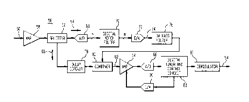
3o A receiver 56 constructed in accordance with the present invention is shown
CA 02228260 1998-O1-30
in FIG. 3. If desired, receiver 56 can be implemented on a digital very large
scale
integrated circuit. Receiver 56 receives radio frequency input signals and
converts them to
an intermediate frequency using conventional techniques. For example, receiver
56 may
use a low noise amplifier, mixer, and bandpass filter such as those shown at
the inputs of
receivers 10 (FIG. 1) and 38 (FIG. 2). The intermediate frequency output of
the receiver is
presented to amplifier 58 at input 60. The levei of the input signal presented
to input 60 is
preferably maintained as high as possible without creating intermodulation
distortion
products. The intermediate frequency input signal is a composite of signals
from multiple
channels. Receiver 56 detects and demodulates the signals on at least one of
these
1o channels. In general, the desired signal or signals may be weak and the
undesired signals
strong.
Sputter 62 is provided to split the output signal from amplifier 58 into paths
64 and 66. The composite signal is essentially unchanged along path 66. In
path 64, the
desired signal is suppressed and the undesired signals inverted, so that when
the signals
from paths 64 and 66 are recombined, the uninverted undesired signals from
path 66 are
cancelled by the inverted undesired signals from path 64. This arrangement
allows the
desired weak signal that remains to be processed using the full dynamic range
of the
receiver amplifier and digitizing circuitry.
The output of sputter 62 along path 64 is digitized by analog-to-digital
2o converter 68, which has a resolution of n bits. Digital notch filter 70 has
coefficients that
can be programmed dynamically to select a center frequency, desired filter
shape, and
desired bandwidth. Notch filter 70 attenuates the desired channel and passes
the remaining
channels unaltered. The output of digital notch filter 70 has m bits of
resolution. The
value of m must be sufficiently large to avoid swamping the notched channel
with
quantization noise.
The quantization noise that is produced in the desired channel by analog-to-
digital converter 68 is subsequently attenuated by digital notch filter 70, so
that it is
generally acceptable for analog-to-digital converter 68 to produce more noise
than digital-
to-analog converter 72. The value of m is therefore generally greater than n.
(If desired,
3o the resolution of analog-to-digital converter 68 can be increased by
increasing the value of
CA 02228260 1998-O1-30
n (even so that n is greater than m), but this is typically unnecessary and
may add cost and
complexity to the overall design.) The quantization noise in the desired
channel after
digital-to-analog converter 72 is determined by the contributions of the noise
output (S)
from notch filter 70 and the quantization noise (M) produced by the m bits of
resolution of
digital-to-analog converter 72. (S is the power due to noise from analog-to-
digital
converter c58 as attenuated by notch filter 70.) Preferably, the magnitude of
S is close to
the magnitude of M. Balancing the noise contributions S and M in this way
utilizes the n
bit resolution of analog-to-digital converter 68, the processing power of
notch filter 71), and
the m bit resolution of digital-to-analog converter 72 to the fullest.
to The output of digital notch filter 70, which contains all of the channels
in
the composite signal except the channel of interest, is provided to digital-to-
analog
converter 72, which generates a corresponding analog output signal at output
74. The
analog output signal is inverted in relation to the composite sib al provided
to path 66.
Lowpass filter 76 is preferably provided to smooth out any signals related to
the clock
oscillator frequencies of digital-to-analog converter 72.
In path 66, delay circuit 78 generates a delay to match the delay introduced
by path 64. (If desired, digital notch filter 70 may provide delay
equalization functions to
assist delay circuit 78 in matching the delay introduced by path 64.) The
unaltered
composite signal from delay circuit 78 is combined with the signal from
lowpass filter 76
2o by combiner 80. The signal at output 82 of combiner 80 is made up primarily
of the
desired signal. The signals in the undesired channels are attenuated to the
level of
quantization noise (i.e., to a maximum of one half of a least significant
bit). The signal at
output 82 is provided to automatic gain control amplifier 84, which can now
use its full
dynamic range to process the desired signal.
The output of amplifier 84 is provided to analog-to-digital converter 86,
which provides a corresponding digital output to digital tuner and control
circuit 88. The
control portion of digital tuner and control circuit 88 is used to adjust the
gain of automatic
gain control amplifier 84 via digital-to-analog converter 90 based on the
amplitudes of the
signals at the input to amplifier 84. The digital tuner portion of digital
tuner and control
3o circuit 88 converts the desired channel to baseband (i.e., to 0 Hz carrier
frequency). Digital
CA 02228260 1998-O1-30
tuner and control circuit 88 preferably also has low-pass circuitry to enhance
the selectivity
of the tuner. During single channel reception, most selectivity is provided by
digital notch
filter 70, v~hich relaxes the requirements for filtering in digital tuner and
control circuit 88.
The output of digital tuner and control circuit 88 is demodulated by
demodulator 92 and
provided at output 94.
The receiver arrangement of FIG. 3 reduces the dynamic range of the signal
provided to amplifier 84, so that the large signal handling requirements of
the amplifier 84
can be relaxed. In addition, the output of amplifier 84 is now almost entirely
made up of
the desired. signal, so that analog-to-digital converter 86 can digitize this
signal with a
to higher resolution than possible when the undesired large signals occupied
the entire
dynamic range of analog-to-digital converter 86.
The ability of receiver 56 to resolve weak channels among strong channels
is particularly useful in environments such as cellular telephone systems. In
cellular
telephone systems, users approaching the edge of a cell are often in
situations in which the
15 desired channel has weaker signals than many of the other channels in the
system.
If desired, receiver 56 can handle multiple channels simultaneously, by
notching out additional channels with notch filter 70 and by modifying digital
tuner and
control circuit 88 and demodulator 92 to tune to and demodulate these
additional channels.
Further, notch filter 70 can weight different channels by different amounts to
compensate
2o for variations in signal strength. For example, a cellular telephone base
station may need
to receive channel 4 (weak) and channel 5 (strong) and may want to suppress
the remaining
channels (strong). With the arrangement of FIG. 2, notch filter 70 can provide
notch
filtering of both channels 4 and 5, simultaneously. Because channel 5 is
strong and
channel 4 is weak, it may be beneficial to filter out channel S only
partially, so that the
25 magnitude of channel 5 at the output of combiner 80 is reduced somewhat.
Balancing the
relative magnitudes of the signals from different channels at the input to
amplifier 84
makes the greatest use of the dynamic range of amplifier 84 and increases the
overall
ability of the system to resolve bath desired channels (4 and 5).
Another capability of receiver 56 is to handle channels of differing
3o bandwidths. Such an arrangement may be useful, for example, in an
environment in which
CA 02228260 1998-O1-30
8
radio station channels are provided using both standard bandwidths and larger
bandwidths
(e.g., to provide compact disc quality audio). The characteristics of digital
notch filter 70
can be selectively varied to accommodate both the narrower and the wider
channels, as
needed. When a regular channel is being received, notch filter 70 suppresses a
regular-
s sized bandwidth channel. When a compact disk quality channel is being
received, notch
filter 70 suppresses a larger-sized bandwidth channel.
The characteristics of receiver 56 can be further illustrated with the
following design example. In this example, two channels are represented by two
carriers
for simplicity. The undesired stronger carrier is Pl having a power level of -
lOdBm. The
to desired weaker carrier is P2 having a power level of -52 dBm (i.e., 42 dB
below the strong
signal). Analog-to-digital converter 68 has 10 bits of resolution (i.e., n=10)
and a full scale
maximum of 400 mV peak-to-peak (one least significant bit (lsb) is equal to
390.625 wV).
Digital-to-analog converter 72 has 16 bits of resolution (i.e., m=16) and
produces an output
of 400 mV peak-to-peak maximum (one Isb equals 6.104 p.V). Digital notch
filter 70 has
15 16 or more bits of resolution.
The -10 dBm (200 mV peak-to-peak) level of P1 is represented by nine bits
of analog-to-digital converter 68 output. The -52 dBm (~1.5 mV peak-to-peak)
level of P2
is represented by 2 bits of analog-to-digital converter 68 output. The maximum
quantization noise power into 50 S2 after analog-to-digital converter 68 is ~-
61.17 dBm
2o maximum, as given by Equation 1.
Max_Quantization Noise Power= (%Z lsb)' / 50 (1)
The ratio of the average signal to the maximum quantization noise for P1 is
51.17 dB and
25 for P2 is 9.17 dB. If digital notch filter 70 attenuates 33 dB in the
desired channel, the
levels for the various stages of receiver 56 using the illustrative design are
as shown in the
table of FI(J. 4.
The output levels at digital-to-analog converter 72 are -10 dBm for P 1
(unchanged) and -85 dBm (attenuated) for P2. When the output of lowpass filter
76 is
3o added to the input signal at combiner 80, P1 is cancelled and the value of
P2 is decreased
CA 02228260 1998-O1-30
9
by -85 darn (-52 dBm - 33 dBm), which results in an output at combiner 80 of -
52.002
dBm, as given by Equation 2.
Output = 10* log (10-'' - 10~~') (2)
Equation 2 demonstrates that in this idealized example the magnitude of the
desired signal at the output of combiner 80 is reduced by a negligible amount.
In practice,
digital-to-analog converter 72 adds quantization noise to the desired signal.
If digital-to-
analog converter 72 has 8 bits of resolution, so that 0.4 V peak-to-peak is
represented by 8
1o bits, the maximum quantization noise level will be -49 dBm. This level is
higher than the
signal level P2, so that P2 will be swamped by quantization noise. (This is
also the case
with 10 bits of resolution.) If however, digital-to-analog converter 72 has 16
bits of
resolution, the maximum quantization noise added by digital-to-analog
converter 72 will
be only -9 7.3 dBm, which is less than the noise level for the desired channel
at the output
of digital notch filter 70. Accordingly, the signal level of P2 at amplifier
84 will have a
signal-to-noise ratio (quantization limited) for the desired signal of 42 dB
(94-52). A 7 bit
analog-to-digital converter 86 will therefore use its full capabilities in
digitizing the desired
weak signal P2. Selecting an appropriate combination of resolutions for
digital-to-analog
converter ~'2 and analog-to-digital converter 86 therefore allows the required
signal-to-
2o noise ratio to be obtained for the desired channel. In the present example,
the weak signal
is resolved to approximately 7 bits. The signal levels seen by amplifier 84
are -52 dBm for
P2 and -61 dBm for P1 (i.e., the strong signal power is at the level of
quantization noise).
Because the undesired composite signals are 9 dB below the desired signal, the
desired
signal can easily be amplified by amplifier 84.
The foregoing is merely illustrative of the principles of this invention and
various modifications can be made by those skilled in the art without
departing from the
scope and spirit of the invention.