Note: Descriptions are shown in the official language in which they were submitted.
CA 02228~07 1998-02-02
r ; !
TITLE OF THE INVENTION
OPTOELECTRONIC MATERIAL, DEVICE USING THE
SAME AND METHOD FOR MANUFACTURING
OPTOELECTRONIC MATERIAL
BAC~GROUND OF THE INVENTION
Field of the Invention
The present invention relates to an
optoelectronic material, its application device and a
10 method of manufacturing the optoelectronic material.
More particularly, this invention relates to an
optoelectronic material that comprises, as the core,
semiconductor ultrafine particles with controlled
particle sizes, formed of a material whose quantity is
15 unlimited and which is free of environmental
contamination, and that is excellent in silicon (Si)-LSI
technology matching, spontaneous light emission, fast
response, pixel miniaturization, low dissipation power,
high environmental resistance and assemblyless process,
20 an application device of the optoelectronic material, and
a method of manufacturing the optoelectronic material.
Description of the Related Art
Conventional light-emitting devices include a
light-emitting diode and devices utilizing
25 electroluminescence which have been put to a practical
use. Optoelectronic materials used for those light-
emitting devices ale compound semiconductors
CA 02228~07 1998-02-02
;~ri
essentially containing a group III element and a group V
element (hereinafter referred to as "group III-V") in a
periodic table or compound semiconductors essentially
containing a group II element and a group VI element in
5 the periodic table, not silicon (Si). This is because
silicon is an indirect transition semiconductor and the
band gap, 1.1 eV, lies in a near infrared region, which has
been considered as impossible to realize a light-emitting
device in a visible light region.
Since the observation of visible light emission of
porous Si at room temperature in 1990 (disclosed in, for
example, L. T. Canham, Applied Physics letters Vol. 57,
No. 10, 1046 (1990)). Enthusiastic studies have been done
on the characteristics of visible light emission at room
15 temperature with Si as a base material. Most of those
reports are concerned with porous Si.
This luminous porous Si is basically formed by
anodization of the surface of a single crystalline Si
substrate in a solution essentially containing hydrogen
20 fluoride, and photoluminescences (PL) of several
wavelengths in a range from 800 nm (red) to 425 nm (blue)
have been observed up to now. Recently, attempts have
been made to luminescence by current injection
excitation (electroluminescence; EL) (e.g., Published
25 Unexamined Application No. 5-206514).
EL of those porous Si have the following
characteristic properties. (1) The spectra of EL and PL
CA 02228~07 1998-02-02
'
show substantially the same shapes with some difference
in intensity though. (2) The EL intensity is
proportional to the injection current in a supposedly
practically usable range of the injection current density.
5 It is to be noted however that in a range where the
injection current density is lower than the former range,
it has been reported that the EL intensity is proportiorlal
to the square of the injection current.
The property (1) indicates that the EL and PL
10 are caused by the recombination of carriers (excited
electron-hole pairs) through approximately same
luminescence levels, and the property (2) indicates that
the generation of carriers essential to EL is mostly
accomplished by the injection of minor carriers in the
15 vicinity of the p-n junction.
With regard to the emission mechanism of Si
which is an indirect transition semiconductor, there are a
view that the wave number selection rule for optical
transition is relaxed in a three-dimensional minute
20 structural area of the nanometer (nm) order in the porous
shape, thus ensuring the radiative recombination of
electron-hole pairs, and a view that a many-remembered
ring oxide (polysiloxene) is formed on the surface of
porous Si and new energy level which contributes to the
25 radiative recombination is formed at the polysiloxene/Si
interface. In any case, it seems certain that with regard
to photo excitation, a change in energy band structure (a
- = -
CA 02228~07 1998-02-02
phenomenon of increasing the gap energy) is caused by
quantum confinement effect.
Further, luminescence from porous Si has a
broad spectrum width of approximately 0.3 eV or wider.
5 In this respect, some attempts have been made to form a
cavity structure using this porous Si in order to enhance
the intensity of a specific wavelength region in the
continuous spectrum that is originally generated (e.g., L.
Pavesi et al., Applied Physics Letters Vol. 67, 3280
(1995)).
Because the conventional optoelectronic
materials use compound semiconductors mainly
consisting a group III-V element or a group II-VI element
of a direct transition type, however, they contain an
15 element (In or the like) whose quantity is significantly
small and whose refining cost is high while the emission
efficiency is high. Further, a fine patterning for those
compound semiconductors as a semiconductor fabrication
technique is not ripe yet as compared with a fine
20 patterning for Si, making it difficult to form a fine
pattern of the micron ( ~L m ) order or smaller.
Furthermore, groupl III and V elements serve as a dopant
in Si, and thus affect the electrical conductivity. That
is, while a spontaneous light-emitting device essentially
25 consists of a semiconductor material, the matching with
the process and device technologies for Si-LSI as a
typical electronic device is poor and it is substantially
-
CA 02228~07 1998-02-02
~r,!
impossible to fabricate a device with integrated Si and
LSI. Moreover, there is an essential problem that the
type of the material should be changed (i.e., it should
newly be found) and the fabrication method should be
5 reconstructed entirely in order to adjust the emission
wavelength.
With regard to luminous porous Si, a porous
layer is formed on the surface of a single crystalline Si
substrate by anodization in a solution so that while a
10 crystalline in the porous layer has an excellent
crystallinity, it is difficult to control the shape and size
of crystalline. It is particularly difficult to efficiently
produce a spherical crystalline of 5 nm or less in particle
size. If the mechanism of visible light emlssion of an
15 Si-based group IV material is a quantum size effect
(relaxation of the wave number selection rule, a change
in band structure due to a quantum confinement effect, or
the like), it is still essential to produce a spherical
crystalline having a particle size of the nm order. In
20 view of this, the fabrication technique cannot be said to
be the optimum one.
A difficulty also arises when one intends to
demonstrate the performance of a display device by
regularly arranging porous Si based light-emitting
25 elements and independently operating them.
Specifically, since the porous Si is directly formed in an
Si substrate, it is not possible to maintain the electric
CA 02228~07 1998-02-02
J,~;!
independence (insulation) between the elements.
Further, it is not possible to form a lamination structure
with another material like a transparent material having
a high transmittance in the visible region.
Although a scheme of arranging particles of a
group IV element or partly oxidized particles thereof
between electrodes for light emission is disclosed (e.g.,
Published Examined Application No. 7-52~70), it has a
difficulty in controlling the electric characteristic and
cannot be adapted to various kinds of light-emitting
devices and photodetectors. Therefore, the state-of-
the-art technology does not provide an optoelectronic
material which can be adapted to various kinds of light-
emitting devices and photodetectors by controlling the
electric characteristics.
SUMMARY OF TIIE INVENTION
It is therefore an object of the present invention
to provide an optoelectronic material that comprises a
material whose quantity is inexhaustive and which is free
of environmental contamination, and has characteristics
such as the Si-LSI technology matching, spontaneous
light emission, fast response, pixel miniaturization, low
dissipation power, high environmental resistance and
assemblyless process, an application device of the
optoelectronic material, and a method of manufacturing
the optoelectronic material.
To achieve this object, an optoelectronic
CA 02228~07 1998-02-02
~J
material according to this invention has ultrafine
particles dispersed in a substantially uniform medium
whose conductivity or dielectric constant is controllable.
This can permit carrier injection in the ultrafine
5 particles or the quantum confinement of carriers in the
ultrafine particles to be accomplished effectively and
controlled.
Further, an optoelectronic material according to
this invention has a periodic structure with an
10 ultrafine-particles dispersed layer and transparent
material layers alternately stacked one on another.
This can provide an optoelectronic material having a
property to enhance the intensity of a specific wavelength
region in the continuous spectrum that is detected or
15 generated by ultrafine particles.
Furthermore, an optoelectronic material
according to this invention has an active layer containing
ultrafine particles, and a high-reflection layer and a
partial reflection layer provided to sandwich the active
20 layer. This can narrow the wavelengths of detected and
emitted lights and can increase the intensity.
Moreover, using any of the aforementioned
optoelectronic materials to constitute a light-emitting
device, a display device or an optoelectric conversion
25 device with a pair of electrodes sandwiching the
optoelectronic material in such a way as to be in direct
contact thereto, it is possible to suitably control the
CA 02228~07 1998-02-02
r~;,
electric contact between the electrodes and the
optoelectronic material layer to effectively accomplish a
light emission or an optoelectric conversion function.
A portable display apparatus according to this
5 invention is designed by essentially using the display
device. This design can provide a potable display
apparatus which is suitable for size and weight reduction
and has low dissipation power and a high resolution, and
which can suitably adapted for use as an HMD or an
10 electronic dictionary.
Further, a method of manufacturing an
optoelectronic material according to this invention
comprises a first target material placing step of placing a
first target material in a vacuum reaction chamber in low
15 pressure rare gas ambient; a second target material
placing step of placing a second target material in a
reaction chamber as isolated from the first target
material and the deposition substrate as an ambient
component; an ablation step of irradiating a laser beam
20 to the first target material placed in the first target
material placing step to cause desorption and injection of
the target material; and an evaporation step of
evaporating the second target material placed in the
second target material placing step. With this
25 structure, a material produced in the evaporation step is
collected on the deposition substrate at substantially the
same timer as ultrafine particles obtained by condensing
I ~1 CA 02228~07 1998-02-02
r~s!
and growing a material, desorbed and injected in the
ablation step, in rare gas ambient are collected on the
deposition substrate to thereby acquire an optoelectronic
material having the ultrafine particles dispersed in a
5 material comprised of the second target material.
BRIEF DESCRIPTION OF THE DRAWINGS
FIGS. lA through lC are cross-sectional
structural views of a light-emitting device according to
the first embodiment of this invention;
FIGS. 2A and 2B are diagrams showing curves of
the current v.s. voltage characteristics of the light-
emitting device;
FIG. 3 is a diagram showing a curve of the
emission intensity v.s. current characteristic of the
15 light-emitting device;
FIG. 4 is a diagram showing a curve on the
emission intensity v.s. duty ratio of the light-emitting
device;
FIG. 5 is a diagram showing curves of the
20 emission intensity v.s. photon energy characteristics of
PL and EL of the light-emitting device;
FIG. 6 is a characteristic chart depicting the
relationship between the particle size of ultrafine
particles and the band gap energy of the light-emitting
25 device;
F'IG. 7 is a cross-sectional structural view of a
light-emitting device according to the second embodiment
CA 02228~07 1998-02-02
~,
~';'
1 0
of this invention;
FIGS. 8A through 8C are structural diagrams of
a monochrome display device according to the third
embodiment of this invention;
FIG. 9 is a structural diagram of a color display
device according to the fourth embodiment of this
nve ntio n;
FIG. 10 is a conceptual diagram showing the
essential structure of a portable display apparatus
10 according to the fifth embodiment of this invention;
FIGS. 1 lA and 1 lB are cross-sectional structural
views of an HMD according to the sixth embodiment of
this invention;
FIG. 12 is a perspective view of the glasses type
1~ HMD mounted;
FIG. 13 is a cross-sectional structural view of an
HMD according to the seventh embodiment of this
invention;
FIG. 14 is a cross-sectional structural view of an
20 optoelectric conversion device according to the eighth
embodiment of this invention;
FIG. 1~ is a cross-sectional structural view of an
optoelectric conversion device according to the ninth
embodiment of this invention;
2~ FIG. 16 is a cross-sectional structural view of a
color sensor according to the tenth embodiment of this
invention;
CA 02228~07 1998-02-02
~';.''
1 1
FIG. 17 shows the absorption spectrum of each
optoelectric conversion layer of the color sensor;
FIGS. 18A and 18B are cross-sectional structural
views of an optoelectronic material according to the
5 eleventh embodiment of this invention;
FIGS. 19A and 19B show emission spectra of the
optoelectronic material shown in FIGS. 18;
FIG. 20 is a cross-sectional structural view of an
optoelectronic material according to the twelfth
10 embodiment of this invention;
FIGS. 21A through 21C are explanatory diagrams
of steps of forming a mixed target according to the
thirteenth embodiment of this invention;
FIG. 22 is a conceptual diagram of an apparatus
15 for preparing ultrafine particles;
FIG. 23 is a characteristic diagram showing the
relationship between a rare gas pressure and the mean
particle size of ultrafine particles;
FIG. 24 is a conceptual diagram of a particle size
20 control apparatus for the ultrafine particles;
FIG. 25 is a conceptual diagram of an apparatus
for manufacturing an optoelectronic material according
to the fourteenth embodiment of this invention;
FIG. 26 is a structural diagram of a hybrid
26 cathode apparatus according to the fifteenth embodiment
of this invention; and
FIG. 27 is a structural diagram of a composite
CA 02228~07 1998-02-02
.,
r~;,
1 2
deposition apparatus for manufacturing the
optoelectronic material.
DETAILED DESCRIPTION OF THE PREFERRED
EMROT)IMENT
An optoelectronic material according to this
invention comprises a uniform medium with a
controllable electric characteristic; and semiconduct~or
ultrafine particles dispersed in the medium and having a
mean particle size of 100 nm or less. This can provide
the quantum confinement effect of ultrafine particles.
It is preferable that the particle size (diameter)
of the semiconductor ultrafine particles in the
optoelectronic material according to this invention or an
ultrafine-particles dispersed layer be equal to smaller
than approximately two times the de Broglie wavelength
of a semiconductor material for the ultrafine particles.
As the optoelectronic material according to this
invention is constituted by dispersing ultrafine particles
are in a medium having a uniform conductivity, the
quantum confinement effect of ultrafine particles can be
demonstrated given without imbalance. Further, As
ultrafine particles are dispersed in a substantially
uniform medium with a controllable conductivity or
dielectric constant, the quantum confinement effect of
carriers in ultrafine particles can be controlled.
It is preferable that the medium have a specific
resistance approximately same as or greater than that of
CA 02228~07 1998-02-02
~' ;!
1 3
the ultrafine particles. This can permit the quantum
confinement effect of carriers in ultrafine particles to be
demonstrated efficiently.
It is also preferable that the distance between
5 the ultrafine particles dispersed in the medium be equal
to or greater than the radius of the ultrafine particles.
Alternatively, the packing fraction of the ultrafine
particles in the medium may be equal to or less than 30%.
This can allow the quantum trapping of ultrafine
10 particles to be demonstrated effectively.
If the standard enthalpy of formation of the
medium is lower than that of an oxide of the ultrafine
particles dispersed in the medium, the ultrafine particles
can stably exist in the medium.
Further, the ultrafine particles dispersed in the
medium may be covered with an oxide of an element
constituting the ultrafine particles. In this case, even
if the standard enthalpy of formation of the medium is
higher than that of an oxide of the ultrafine particles
20 dispersed in the medium, the ultrafine particles can
stably exist in the medium.
It is suitable that the ultrafine particles in the
above-described optoelectronic materials contain a group
IV semiconductor. With this structure, ultrafine
25 particles are formed of a material whose quantity is
unlimited and which is free of environmental
contamination, and are excellent in Si-LSI technology
CA 02228~07 1998-02-02
.
~; !
matching, environmental resistance and assemblyless
process. The ultrafine particles may contain a group
III-V or II-VI compound semiconductor. Further, the
medium is suitably a thin film of transparent conductive
5 material or dielectric material.
An optoelectronic material according to this
invention is characterized by the structure where an
ultrafine-particles dispersed layer having semiconductor
ultrafine particles with a mean particle size of 100 nm or
10 less dispersed in a uniform medium with a controllable
electric characteristic, and transparent material layers
are alternately stacked one on another. This can
enhance the intensity of a specific wavelength region in
the continuous spectrum that is inherently generated by
15 ultrafine particles.
The transparent layers are suitably formed of a
thin transparent conductive film or dielectric film. It is
desirable that the ultrafine-particles dispersed layer has
the aforementioned characteristics.
An optoelectronic material embodying this
invention comprises an ultrafine-particles dispersed
layer having semiconductor ultrafine particles with a
mean particle size of 100 nm or less dispersed in a
uniform medium with a controllable electric
25 characteristic; and a partial reflection layer and a
high-reflection layer provided on and under the
ultrafine-particles dispersed layer. This can enhance
. == ~
CA 02228~07 1998-02-02
1 5
the intensity of a specific wavelength region in the
continuous spectrum that is inherently generated by
ultrafine particles. At least one of the partial
reflection layer and the high-reflection layer may be
5 formed of a thin metal film.
It is preferable that at least one of the partial
reflection layer and the high-reflection layer should have
a multilayer structure with a periodic structure having
at least two kinds of layers with different refractive
10 indexes alternately stacked one on another. This can
enhance the intensity of a specific wavelength region in
the continuous spectrum that is inherently generated by
ultrafine particles contained in the ultrafine-particles
dispersed layer.
Alternatively, the high-reflection layer may be
formed of a multilayer film having at least two kinds of
layers with different refractive indexes alternately
stacked one on another, and a thin metal film. The
multilayer film may include an ultrafine-particles
20 dispersed layer having the aforementioned
characteristics.
It is preferable that the ultrafine-particles
dispersed layer in the above-described optoelectronic
material should have the aforementioned characteristics.
~5 In this case, the optical film thickness of the ultrafine-
particles dispersed layer is suitably an integer multiple
of the wavelength of the emitted light.
CA 02228~07 1998-02-02
1 6
A light-emitting device according to this
invention comprises an ultrafine-particles dispersed
layer having semiconductor ultrafine particles with a
mean particle size of 100 nm or less dispersed in a
uniform medium with a controllable electric
characteristic; and a pair of electrodes sandwiching the
ultrafine-particles dispersed layer, whereby as a voltage
is applied to the pair of electrodes, carriers are injected
into the semiconductor ultrafine particles and light
10 emission occurs in a radiative recombination of
electron-hole pairs caused by carrier injection. This
can permit the electric connection between the electrodes
and the optoelectronic material layer to be controlled.
The emitted photon energy may be controlled by
15 adjusting the particle size of ultrafine particles, or by
adjusting the surface atomic arrangement of ultrafine
particles. It is suitable that the pair of electrodes are
transparent or semitransparent electrodes, which can
provide excellent transmittance of external light.
Further, a thin film of a metal electrode may
contact the ultrafine-particles dispersed layer. In this
case, it is preferable that the ultrafine-particles
dispersed layer and the metal electrode should have a
Schottky junction type contact. The thin film of a metal
25 electrode suitably contains any one of magnesium, indium,
aluminum, platinum, gold, silver, tungsten, molybdenum,
tantalum, titanium, cobalt, nickel and palladium.
CA 02228~07 1998-02-02
i.
';.'
1 7
Further, it is suitable that a semiconductor
substrate provided with one electrode and an insulator
layer formed on the one-electrode side of the
semiconductor substrate and having an opening for
partially exposing the semiconductor substrate are
provided, an optoelectronic material layer is formed to
cover the opening to make the opening portion an active
region, the radiative recombination of electron-hole pairs
inside ultrafine particles or in the vicinity of the surface
of the ultrafine particles is accomplished by a
multiplication phenomenon, and the emission intensity
has such a property as to increase more than being
proportional to an injection current to the light-emitting
device. The use of such a multiplication phenomenon
can ensure very effective utilization of power to be
consumed in the initial electron injection and the limited
quantum efficiency at the time of ion impact, and is
significantly effective in increasing the dynamic range of
the emission intensity.
If p-n junction is formed in the optoelectronic
material layer, a high power efficiency is ensured as
compared with the case where it merely has a Schottky
junction type contact which apparently is the simplest
structure to realize a light-emitting device.
A monochrome display device for adjusting the
emission intensity of each of unit pixels, regularly
arranged in a planar form, by a change in the excitation
CA 02228~07 1998-02-02
~'; '
1 8
current to the light-emitting elements of the unit pixels
by using such light-emitting elements to form light-
emitting elements corresponding to the unit pixels. A
color display device for adjusting the emission intensity
5 and color of each of unit pixels, regularly arranged on a
plane, by a change in the excitation current to light-
emitting elements constituting the unit pixels may be
constituted by designing light-emitting element designed
to have ultrafine particles with different mean particle
10 sizes so as to emit lights of different colors in the three
primary colors, and using the light-emitting elements to
form light-emitting elements which correspond to the
unit pixels and are capable of emitting all of the three
primary colors.
This invention further provides a portable
display apparatus having the above-described display
devices. In this case, a very high resolution can be
obtained by setting the length of the unit pixels in on
direction to about 1 to 100 ~ m . The portable display
20 apparatus having such display devices may be a head
mounted display which comprises a fixing member for
securing the display apparatus to a head of a person
whom the display device is to be mounted, and an optical
system for forming information displayed on the display
25 device to right and left eyes of the person. With this
structure, the display apparatus is compact and provides
high definition, so that the eye contact optical system
CA 02228~07 1998-02-02
;.'
1 9
becomes compact, thus contributing to reducing the size
and weight of the main body of the head mounted display
and ensuring a wide view angle and high resolution.
The optical system of the head mounted display
may also form outside information on the right and left
eyes of the person wearing the display. It is preferable
that the light-emitting devices having the transmittance
should be laid out on a transmittive member to have the
transmittance so that outside light is introduced to the
optical system. Because of the transmittance, this
structure can realize a compact see-through type head
mounted display which does not require a half mirror or
the like.
The display devices may be arranged in a
direction of a line of sight different from an outward line
of sight of the person wearing the apparatus, so that the
person can easily observe outside by shifting the line of
sight up and down or the like, not moving the head itself.
This invention also provides an electronic
dictionary which displays information by means of the
display devic.es. As the display apparatus is compact
and high definition type, it is possible to realize a
compact and light dictionary which has the same level of
high resolution as conventional paper dictionaries.
26 A photodetector according to this invention
comprises an ultrafine-particles dispersed layer having
semiconductor ultrafine particles with a mean particle
CA 02228~07 1998-02-02
r~;~
2 0
size of 100 nm or less dispersed in a uniform medium with
a controllable electric characteristic; and a pair of
electrodes sandwiching the ultrafine-particles dispersed
layer, and has a photodetective function by detecting a
5 change in an internal resistance caused by carrier
generation originated from light irradiation to the
ultrafine-particles dispersed layer.
A photodetector according to this invention
comprises an optoelectronic material layer containing the
10 aforementioned optoelectronic material, and a pair of
electrodes provided on and under the optoelectronic
material layer, with Schottky junction formed at an
interface between the optoelectronic material layer and
the electrodes or p-n junction formed in the
15 optoelectronic material layer, and has a photodetective
function by detecting a change in photoelectromotive
force generated by carrier generation originated from
light irradiation.
The emitted photon energy may be controlled by
20 adjusting the particle size of ultrafine particles, or by
adjusting the surface atomic arrangement of ultrafine
particles.
An optoelectric conversion device according to
this invention is an optoelectric conversion device, which
25 comprises an optoelectronic material layer containing the
aforementioned optoelectronic material, and a pair of
electrodes provided on and under the optoelectronic
CA 02228~07 1998-02-02
;,~;.
2 1
material layer, and which has a function of exhibiting a
light emission in a radiative recombination of generated
electron-hole pairs caused by carrier injection when
minor carriers are injected into the ultrafine particles of
5 the optoelectronic material layer through the pair of
electrodes, and a photodetective function by detecting a
change in an internal resistance caused by carrier
generation when light is irradiated on the optoelectronic
material layer.
An optoelectric conversion device according to
this invention is an optoelectric conversion device, which
comprises an optoelectronic material layer containing the
aforementioned optoelectronic material, and a pair of
electrodes provided on and under the optoelectronic
1~ material layer, with Schottky junction formed at an
interface between the optoelectronic material layer and
the electrodes or p-n junction formed in the
optoelectronic material layer, and which has a function of
exhibiting a light emission in a radiative recombination
20 of generated electron-hole pairs caused by carrier
injection when minor carriers are injected into the
ultrafine particles of the optoelectronic material layer
through the pair of electrodes, and a photodetective
function by detecting photoelectromotive force generated
2~ by carrier generation when light is irradiated on the
optoelectronic material layer.
The emitted and detected photon energy may be
CA 02228~07 1998-02-02
. '
t !; ~
2 2
controlled by adjusting the particle size of ultrafine
particles, or by adjusting the surface atomic arrangement
of ultrafine particles.
In the above-described optoelectric conversion
5 devices, a pair of electrodes may be transparent or
semitransparent electrodes.
By controlling optical gap energy by adjusting
the mean particle size of the ultrafine particles in the
aforementioned photodetector or the structure of the
10 surface atomic arrangement, the photodetector according
to this invention can be used as an ultraviolet detector
comprising a photodetector having a photodetective
function for ultraviolet rays. This structure eliminates
the need for filters or the like and provides excellent
15 characteristics in the Si-LSI technology matching,
environmental resistance and assemblyless property.
By controlling optical gap energy by adjusting
the mean particle size of the ultrafine particles in the
aforementioned photodetector or the structure of the
20 surface atomic arrangement, this invention provides a
blue-color sensor comprising a photodetector having a
photodetective function for blue light. This structure
eliminates the need for filters or the like and provides
excellent characteristics in the Si-LSI technology
25 matching, environmental resistance and assemblyless
property.
By controlling optical gap energy by adjusting
CA 02228~07 1998-02-02
2 3
the mean particle size of the ultrafine particles in the
aforementioned photodetector or the structure of the
surface atomic arrangement, this invention provides a
color sensor comprising optoelectric conversion layers,
comprised of the photodetectors having photodetective
functions in different predetermined wavelength regions,
stacked through a transparent insulator film. With this
structure, when light is irradiated, only the
optoelectronic material layer which has a sensitivity to
10 its wavelength component performs optoelectric
conversion, thus providing the function of a color sensor.
It is suitable in view of the light-receiving
sensitivity that the stacked photoelectric conversion
layers have different optical gap energies and the layer
15 closer to the light-receiving surface has a greater optical
gap energy. Further, the photoelectric conversion
layers may include three photoelectric conversion layers
which have different optical gap energies in the visible
light region.
This invention provides a monolithic integrated
semiconductor device which has at least one or more of
the aforementioned light-emitting device, display device,
optoelectric conversion device, ultraviolet detector,
blue-color sensor and color sensor. With this structure,
25 the device is formed of a material whose quantity is
unlimited and which is free of environmental
contamination, and has excellent characteristics in the
CA 02228~07 1998-02-02
~i;,
2 4
Si-LSI technology matching, environmental resistance
and assemblyless property.
A method of manufacturing an optoelectronic
material according to this invention is characterized in
5 that a laser beam is irradiated onto a first target of a
semiconductor material, placed in a reaction chamber in
low pressure rare gas ambient, a semiconductor material
ablated from the first target is condensed/grown to
acquire ultrafine particles having a mean particle size of
10 100 nm or smaller, and the ultrafine particles are
enclosed in a medium material having a controllable
electric characteristic. Schemes for causing the
ultrafine particles to be enclosed in a medium material
having a controllable electric characteristic include a
15 laser ablation and a scheme of burying ultrafine particles
in a medium material formed in a bulk.
That is, the method is characterized by placing a
first target material in a vacuum reaction chamber in low
pressure rare gas ambient, placing a deposition substrate
20 in the vacuum reaction chamber, and irradiating a laser
beam to the first target material placed in the first
target material placing step to cause desorption and
injection of the target material (ablation), and collecting
ultrafine particles, obtained by condensing and growing a
25 material, desorbed and injected in this ablation step, in
rare gas ambient on the deposition substrate to acquire
an optoelectronic material containing the ultrafine
CA 02228~07 1998-02-02
Y
; ~ ; ''
2 5
particles.
With the above-described structure, ultrafine
particles with the particle size controlled on the nm order
are surely deposited on the substrate by performing the
5 laser ablation step in rare gas ambient.
A method of manufacturing an optoelectronic
material according to this invention comprises a step of
irradiating a laser beam onto a first target of a
semiconductor material, placed in a reaction chamber in
10 low pressure rare gas ambient, and a second target of a
medium material with a controllable electric
characteristic, placed in the reaction chamber, and
condensing/growing a semiconductor material ablated
from the first target to be collected as ultrafine particles
15 having a mean particle size of 100 nm or smaller on a
substrate placed in the reaction chamber, and
condensing/growing a medium material ablated from the
second target to be collected on the substrate placed in
the reaction chamber, thus forming an ultrafine-particles
20 dispersed layer having semiconductor ultrafine particles
dispersed in the medium on the substrate.
The method according to this invention places a
second target material in the vacuum reaction chamber
where the first target material is placed, and sputters
25 the second target material to collect a material, produced
by sputtering, on the deposition substrate at
substantially the same time as ul~rafine particles
CA 02228~07 1998-02-02
2 6
obtained by condensing and growing a material, desorbed
and injected in the ablation step, in rare gas ambient are
collected on the deposition substrate to thereby acquire
an optoelectronic material having the ultrafine particles
5 dispersed in a material comprised of the second target
material. With this structure, a thin dielectric film
with dispersed ultrafine particles is formed on the
substrate by simultaneous deposition using ablation and
sp uttering.
Further, a method according to this invention
places a first target material in a first reaction chamber
in low pressure rare gas ambient, places a deposition
substrate in a deposition chamber, places a second target
material in a second reaction chamber as isolated from
15 the first target material and the substrate as an ambient
component, irradiates a laser beam to the first target
material placed in the first target material placing step
to cause desorption and injection of the target material
(ablation), and evaporates the second target material
20 placed in the second target material placing step. With
this structure, a material produced in the evaporation
step on the second target material is collected on the
deposition substrate at substantially the same time as
ultrafine particles obtained by condensing and growing a
25 material, desorbed and injected in the ablation step on
the first target material, in rare gas ambient are
collected on the deposition substrate so that an
CA 02228507 1998-02-02
;, ?;,
2 7
optoelectronic material having the ultrafine particles
dispersed in a material comprised of the second target
material can be acquired.
It is preferable that a laser be used in the
5 evaporation step for evaporating the second target
material, and ablation of irradiating a second laser beam
to the second target material to cause desorption and
injection of the target material may be used.
It is preferable that the above-described method
10 of manufacturing an optoelectronic material should
further comprise a step of changing introduction pressure
of a low pressure rare gas, and this structure can permit
a mean particle size of the ultrafine particles to be
controlled.
A step of performing mass separation of
ultrafine particles acquired from the ablation step may
further be provided. This structure can allow a mean
particle size of the ultrafine particles to be controlled.
In this case, the step of performing mass separation of
20 ultrafine particles may include a step of ionizing
ultrafine particles and a step of applying an electric field
or a magnetic field to the ionized ultrafine particles.
In the above method, the first target material
may include at least one of a semiconductor, metal and
25 dielectric substance. Further, t.he first target material
may be a mixed material containing a plurality of group
IV semiconductors, and this mixed material may be a
CA 02228~07 1998-02-02
~.
2 8
mixture of silicon and germanium and in a mixed crystal
state. With this structure, by using mixed crystal
ultrafine particles, a mixed crystal composition ratio can
be used as an auxiliary parameter in adjusting the light
5 emission characteristics. Furthermore, such mixed
crystallization facilitates the relaxation of the wave
number selection rule at the time of making ultrafine
particles, or facilitates the occurrence of radiative
recombination.
It is suitable that the mixed material is formed
by a mixing step of mechanically mixing plural types of
starting row particles and a sintering step of sintering
the mixed particles by hot press.
With the first target material being a group II-
15 VI semiconductor or a group III-V semiconductor, the
laser ablation method is basically a process which does
not depend much on the melting point of the target
element or the evaporation pressure, so that those
semiconductor ultrafine particles with the stoichiometric
20 composition maintained can be fabricated.
Further, a step of introducing an n-type
conductive impurity and a p-type conductive impurity to
a semiconductor layer formed by the ultrafine particles
collected on the deposition substrate may be provided, so
25 that p-n junction is formed in the semiconductor layer.
In this case, the n-type conductive impurity and p-type
conductive impurity to be introduced in the
CA 02228~07 1998-02-02
~i;,'
2 9
semiconductor layer may be introduced at different
diffusion depths, so that p-n junction can be formed at
the desired position.
It is suitable that the second target material is a
5 transparent conductive material or dielectric material.
Further, a step of oxidizing the surface of the
optoelectronic material on the substrate may be provided.
This structure eliminates a surface layer in which crystal
defect or impurity is mixed and improves the
10 crystallinity and purity. It is suitable that in the
oxidization step, ultrafine particles acquired in an air
association step are subjected to a heat treatment in an
ambient gas containing oxygen to thereby coat surfaces of
the ultrafine particles with a thermal oxide film. It is
15 also suitable that a heat treatment in a non-oxidization
ambient at a higher temperature than a temperature at a
time of forming a thermal oxide film in a coating step is
carried out prior to formation of the thermal oxide film,
which can recover the crystallinity of ultrafine particles
20 more completely.
This invention provides an optoelectronic
material fabricated by the above-descrlbed method of
manufacturing optoelectronic material. This structurc
can provide an ultrafine-particles dispersed material
25 with the particle size of ultrafine particles controlled.
This invention also provides an ultrafine-particles
dispersed layer or an optoelectronic material layer
CA 02228~07 1998-02-02
3 0
formed of an optoelectronic material fabricated by the
above-described method of manufacturing optoelectronic
material. This structure can provide an ultrafine-
particles dispersed material with the particle size of
5 ultrafine particles controlled.
This invention provides a light-emitting device
whose optoelectronic material layer is comprised of an
optoelectronic material obtained by the above-described
method. Further, this invention provides a monochrome
10 display device or a color display device including the
mentioned light-emitting device. Furthermore, this
invention provides a portable display apparatus having
the mentioned display device.
This invention provides an optoelectric
16 conversion device whose optoelectronic material layer is
comprised of the aforementioned optoelectronic material.
Further, this invention provides an ultraviolet detector
and a blue-color sensor both comprising the mentioned
optoelectric conversion device. Furthermore, this
20 invention relates to a color sensor comprising the
mentioned optoelectric conversion device.
Moreover, this invention provides a monolithic
integrated semiconductor device which has at least one or
more of the aforementioned light-emitting device, display
25 device, optoelectric conversion device, ultraviolet
detector, blue-color sensor and color sensor.
First Embodiment
CA 02228~07 1998-02-02
..
3 1
The principle structure of a light-emitting
device using an optoelectronic material according to this
invention will now be described in detail as the first
embodiment with reference to FIGS. 1 through 5.
According to this embodiment, a description will
be given of an electroluminescence (EL) device in which a
light-emitting (active) region is an optoelectronic
material layer having ultrafine particles of Si, a typical
one of group IV semiconductors, with its surface covered
with its own thermal oxide film, dispersed in a
substantially uniform transparent medium with a
controllable conductivity or dielectric constant.
In this embodiment and subsequent embodiments,
the "substantially uniform medium" means the electric
properties of a medium, particularly, the conductivity is
approximately uniform in the medium. That is,
ultrafine particles to be dispersed in a medium are a set
of several tens to several hundreds of atoms/molecules,
whereas a medium itself consists of a set (cluster) of
smaller atoms/molecules or of several atoms/molecules.
For example, this uniform medium is acquired by forming
a uniform film, comprised of a set (cluster) of
atoms/molecules smaller than those of ultrafine particles
or of several atoms/molecules, on a predetermined
substrate or the like by a method such as deposition. In
this case, uniform deposition of the cluster on the
substrate can be accomplished by adjusting the
CA 02228~07 1998-02-02
~' ;.''
3 2
differential pressure in reaction chambers, e.g., the
differential pressure between a reaction chamber and a
deposition chamber, by a method like a laser ablation
scheme to be discussed later.
In this invention, when the packing fractions of
ultrafine particles in arbitrary minute regions
(containing about ten ultrafine particles, for example)
extracted are confirmed to be equal, it is called a uniform
transparent ultrafine-particles dispersed medium. The
formation of such a uniform transparent ultrafine-
particles dispersed medium suppresses the distribution
width of the kinetic energy of electrons, thus ensuring
efficient light emission.
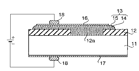
FIG. 1 shows the cross-sectional structure of a
light-emitting device using an optoelectronic material
according to this embodiment. In FIG. lA, " 11" is a
substrate. As this substrate 11, an n-type Si substrate
having a plane orientation (100), a phosphorus-doped n-
type conductivity, and a specific resistance of 10 Q ~ cm
was used as one example. An isolation insulator film 12,
which is a silicon oxide (SiO~) film as one example, is
formed 100 nm thick on the top surface of this n-type Si
substrate. This isolation insulator film 12 has an
opening 12a of about 1 to 2 mm or smaller in diameter
formed at the portion which should be the light-emitting
(active) region of the light-emitting device, exposing the
surface of the substrate 11.
CA 02228~07 1998-02-02
.~
r '; .
3 3
An optoelectronic material layer 13 is deposited
so as to cover at least the opening 12a. This
optoelectronic material layer 13, as shown in FIGI. lB, is
formed of Si ultrafine particles 14 dispersed in a
5 transparent medium 15. The Si ultrafine particles 14
have substantially spherical shapes, the same crystal
structure as bulk Si, an n-type conductivity with
phosphorus doped at a low concentration, and an adjusted
particle size of about 3 to 10 nm. This ultrafine-
10 particles deposition layer has a thickness of about 150nm. Further, the surfaces of the Si ultrafine particles
14 are covered with an unillustrated SiO2 film whose
thickness should be 3 nm or thinner, for example. As
the optoelectronic material layer 13 and the substrate 11
15 are both of an n-type, an electric barrier is not formed at
the interface between them.
The transparent medium 15 is a thin uniform
film which has a high transmittance in the visible light
region and has a controllable conductivity or dielectric
20 constant, and a thin tin oxide (SnO2) film was used here
as one example. This thin SnO2 film has a visible light
transmittance of more than 80%, and its conductivity or
dielectric constant can be controlled by adjusting it
forming conditions (substrate temperature, a partial
25 pressure of oxygen, etc.). It is suitable that the specific
resistance of the medium is about the same as, or equal to
or greater than, the specific resistance of ultrafine
CA 02228~07 l998-02-02
3 4
particles to be dispersed. For example, since the
specific resistance of ultrafine particles lies in the range
of about 10 to 10- 3 Q cm due to the impurity
concentration, the specific resistance of the thin SnO2
5 film has only to be controlled in the range of about 103 to
10-2 Q ~ cm in accordance with the specific resistance of
the ultrafine particles to be dispersed. Such a specific
resistance can be achieved by forming the thin SnO2 film
at the substrate temperature ranging from, for example,
10 room temperature to about 600 ~C The above can permit
the quantum confinement effect of carriers in the
ultrafine particles to be controlled.
It is desirable that the packing fraction of the Si
ultrafine particles 14 in the optoelectronic material layer
15 13 should be higher because the amount of light emission
from the entire optoelectronic material layer 13 increases
When the packing fraction become higher or the distances
between the ultrafine particles become closer, however,
the wave functions of the carriers in the ultrafine
20 particles become wider and the carriers permeate into the
transparent medium too, so that overlapping of the wave
functions of the carriers in the adjoining ultrafine
particles becomes larger. Consequently, the quantum
confinement effect of the carriers in the ultrafine
25 particles is reduced. It is therefore desirable that
dispersion should be performed with the distances
between the ultrafine particles maintained in such a way
CA 02228~07 l998-02-02
v
r'';.
3 5
that the overlapping of the square of the absolute values
of the wave functions become, for example, equal to or
smaller than a hundredth of the peak value. This
distance is equivalent to the radius r of the ultrafine
5 particles. In this case, given that spherical ultrafine
particles having a radius of 1.5r have a close-packed
structure, the packing fraction becomes about 22%. In
view of the above, the packing fraction of the Si ultrafine
particles 14 in the optoelectronic material layer 13 was
10 set to approximately 20%.
A semitransparent electrode 16 of platinum (Pt)
and 10 nm in thickness, as one example, contacts the top
surface of the optoelectronic material layer 13, forming
so-called Schottky contact, in an electric sense, to the
15 optoelectronic material layer 13 including the
transparent medium 15 with the controlled conductivity.
A backside electrode 17 of silver (Ag) as one example is
provided at the bottom surface of the substrate 11,
forming ohmic contact, in an electric sense, to the
20 substrate 11. Further, a thin magnesium (Mg) film
having a thickness of about 20 nm may be provided
between the substrate 11 and the backside electrode 17 to
reduce the electric barrier height at the interface. The
electrodes 16 and 17 may be formed, instead of Pt and Ag,
25 of one of Mg, indium, aluminum, gold, silver, tungsten,
molybdenum, tantalum, titanium, cobalt, nickel and
p alladium .
CA 02228~07 1998-02-02
r'~ ;.
Although Si is used as a material for the
ultrafine particles whicll constitute the optoelectronic
material layer, another group IV semiconductor, such as
germanium (Ge) or its mixed crystal, is suitably used, or
5 a group III-V or a group II-VI compound semiconductor
may be used. While a thin SnOz has been used as the
uniform transparent medium, another thin dielectric film
having a specific resistance substantially the same as, or
greater than, the specific resistance of ultrafine
10 particles to be dispersed, such as a thin film of titanium
oxide (TiO5,), indium oxide (InO2), indium-tin oxide (ITO),
cadmium oxide (CdO), tungsten oxide ( WO 3), ZillC oxide
(ZnO), magnesium oxide (MgO) or ZillC sulfide (ZnS), may
be used as well. If the film thickness lies in the range
15 where electric conduction by tunneling or hopping is
possible, a thin dielectric film of SiO2, aluminum oxide
(Al2O3), magnesium fluoride (MgF2) or calcium fluoride
(CaF2), can be used as well.
Although Si ultrafine particles are covered with
20 their own thermal oxide film here, the oxide film of the
ultrafine particles is not essential. That is, when the
standard enthalpy of formation of the transparent
medium is lower than the standard enthalpy of formation
of the oxide of the ultrafine particles constituting the
25 optoelectronic material layer, which means that the
transparent medium is more stable, oxidization does not
occur when the ultrafine particles are dispersed in the
CA 02228~07 1998-02-02
r';.
3 7
transparent medium, thus eliminating the need of the
oxide film. When the transparent medium has a higher
standard enthalpy of formation, on the other hand, it
means that the oxide of the ultrafine particles is more
5 stable. When the ultrafine particles are dispersed in
the transparent medium, therefore, the surface of the
ultrafine particles is oxidized while reducing the
transparent medium. In this case, therefore, it is
preferable that the ultrafine particles should be covered
10 with an oxide film before they are dispersed in the
transparent medium.
Specifically, typical combinations of the
materials for ultrafine particles constituting an
optoelectronic material and the transparent medium are
15 given in Table 1. In Table 1, combinations A are for the
case where the transparent medium has a lower standard
enthalpy of formation so that the oxide film of the
ultrafine particles is unnecessary. By contrast,
combinations B are for the case where the standard
20 enthalpy of formation of the transparent medium is
higher than that of the oxide film of the ultrafine
particles, so that the ultrafine particles should
preferably be covered with the oxide film.
Table 1
Transparent Medium Ultrafine
P article s
CA 02228~07 1998-02-02
;?;~
3 8
s
Ge
Al203 A
A
TiO 2 A
A
In203 A
A
SiO~ A
10 A
WO2 B
A
MgO B
A
SnO2 B
B
ZnO B
B
CdO B
20 B
The operational characteristics of an EL device
with the above-described structure will be discussed
below.
For the operation of the EL device according to
25 this embodiment, a negative DC bias is applied to the
backside electrode 17 with respect to the
semitransparent electrode 16. This means that the
CA 02228~07 l998-02-02
rZ;!
3 9
light-emitting device of this embodiment operates on the
forward bias.
FIGS. 2 show curves of the current v.s. voltage
characteristics of the light-emitting device when the
5 light-emitting device using the optoelectronic material
according to this embodiment is operated under such a
condition.
FIG. 2A shows both the vertical scale (current)
and horizontal scale (voltage) in linear scale; for the
10 applied voltage on the horizontal scale, the forward bias
potential at the Schottky junction formed at the interface
between the semitransparent electrode 16 and the
optoelectronic material layer 13 in FIG. 1 is taken as the
positive direction on the graph. FIG. 2A shows a strong
15 rectifying characteristic by the Schottky junction formed
at the interface between the semitransparent electrode
16 and the optoelectronic material layer 13. An
external series resistance of the entire light-emitting
device, as estimated through extrapolation on the high
20 current side at the time of the forward bias voltage is
applied, is approximately 400 Q.
FIG. 2B shows only the vertical scale (current)
in logarithmic scale and the horizontal scale (voltage) in
linear scale with the forward bias potential at the
25 Schottky junction taken as the positive direction on the
graph. From the inclination of this characteristic curve
in this figure, the value of the ideal factor n of Schottky
CA 02228~07 1998-02-02
~7
;;;,
4 0
junction can be acqulred. It is however apparent that'as
the value n of the light-emitting device according to this
embodiment depends on the applied voltage, it is 1.8
when the applied voltage is 0.2 V or lower, and is
5 increased to about 15 for a higher area. In general, a
high value of n significantly greater than 1 means that
the interface level density is high and they are charged.
In view of this point too, it appears that the EL device
according to this embodiment of the invention emits light
10 when a forward bias voltage is applied to the Schottky
junction formed at the interface between the
semitransparent electrode 16 and the optoelectronic
material layer 13.
FIG. 3 shows a curve of the emission intensity
15 v.s. current characteristic of the EL device which uses
the optoelectronic material according to this embodiment.
In the figure, both the vertical scale (emission intensity)
and the horizontal scale (current) are shown in
logarithmic scale. It is understood from FIG. 3 that
20 light emission starts when the forward bias current
density is 30 mA/cm2 (the forward bias voltage is about
7.0 V in this case) after which the emission intensity
monotonously increases with an increase in forward bias
current. That is, the emission intensity IEL and the
25 forward bias current j are expressed by the following
equation (1).
IEL oc j (m = 3.5) (1)
CA 02228~07 1998-02-02
Si
4 1
The emission intensity being proportional to the
power 3.5 of the forward bias current means that the
dependency of the emission intensity on the forward bias
current is very sharp, which is a novel result that has not
5 been observed at all in the conventional light-emitting
devices having crystalline Si as an active layer. In an
EL device having a porous Si layer as an active region, for
example, as has been discussed in the section of
BACKGROUND ART, basically, the emission intensity
10 merely increases in proportion to the forward bias
current (the broken line in the figure). The abrupt
dependency of the emission intensity on the forward bias
current means that a light-emitting/display device with a
large dynamic range, i.e., a high contrast ratio, and high
15 quality can be realized.
FIG. 4 shows a curve of the emission intensity
v.s. duty ratio of the EL device according to this
embodiment. In the figure, both the vertical scale
(emission intensity) and the horizontal scale (duty ratio)
20 are shown in logarithmic scale. The applied voltage to
the EL device had a pulse width of 20 ~ s and a voltage
value of 32 V, and the duty ratio was changed from 0.25%
to 100% (DC) by changing the frequency. It is apparent
from FIG. 4 that the emission intensity decreases in
25 proportion to a reduction in duty ratio. This result
shows that the light emission efficiency is constant. In
other words, it can be said that the EL device according
CA 02228~07 1998-02-02
4 2
to this embodiment is hardly affected by heat generated
inside the EL device. Since the same light emission
efficiency as that for DC can be acquired even when the
EL device is driven with a pulse width of 20 ~L s or
narrower, the device can be said to have a response speed
on the order of ~ s or faster.
FIG. 5 shows spectra (curves of the emission
intensity v.s. photon energy characteristics) of both
photoluminescence (PL~ and EL of the EL device using the
10 optoelectronic material according to this embodiment.
Excitation of PL was conducted by using an argon ion
(Ar+) laser with photon energy of 2.54 eV and power of 10
mW and directly irradiating a laser beam to the
optoelectronic material layer which would become the
15 active layer. The excitation conditions for EL were
injection power of 0.55 W to 1.10 W to the optoelectronic
material layer and the luminescence active region being
circular (3.1 x 1 o 2 cm2).
FIG. 5 shows that PL has a spectrum having the
20 main peak at 2.10 eV (green) and a subpeak at 1.65 eV
(red), whereas EL has a broad luminescence spectrum
with the peak of 1.65 eV (red). The peak position of the
EL spectrum shifts toward the lower energy side as
injection power to the EL device increases.
The results indicate that the principle of light
emission of the EL device usimg the optoelectronic
material according to this embodiment is not based on
CA 02228~07 1998-02-02
4 3
black body radiation. This is because the radiation
peak shifts toward the higher energy as the temperature
rises in black body radiation, whereas, as mentioned
above, it shifts toward the lower energy as the injection
5 power increases (i.e., the temperature rises) in this
embodiment. Further, when a black body emits light
having a peak at 1.66 eV, the temperature is estimated to
be 3800 K, and the temperature cannot reach that high in
this embodiment.
It seems that the operational principle of the
light-emitting device according to this embodiment which
shows the aforementioned results is explained as f~llows.
First, hot electrons accelerated by the forward bias
applied voltage are injected to the optoelectronic
15 material layer 13. The injected hot electrons, when
reaching the core of the Si ultrafine particles 14, excite
(generate) electron-hole pairs by impact ionization.
The quantum efficiency in this excitation process reaches
about 1.0 when the energy of the injected electrons is 4.0
20 eV, and goes up as the energy further increases.
The electrons once injected or the electron-hole
pairs once excited are confined inside the Si ultrafine
particles 14 by the interface between the Si ultrafine
particles 14 and the SiO2 film formed on their surface or
25 the transparent medium 15, to further generate
electron-hole pairs in the applied voltage in the Si
ultrafine particles 14. That is, a so-called
CA 02228S07 1998-02-02 r
4 4
multiplication phenomenon occurs to further generate
multiple excited electron-hole pairs. The light emission
phenomenon with an abrupt dependency of the emission
intensity on the forward bias current i8 therefore caused
6 by the recombination phenomenon around the radiative
recombination associated with the excited electron-hole
pairs which are kept generated in such a multiplication
m a n n e r .
In addition, since the target Si ultrafine
10 particles 14 have spherical shapes of the nm order
according to this embodiment, the mean free path of the
electrons or excited electron-hole pairs confined in the
ultrafine particles 14 is short, which, it seems, can
generate excited electron-hole pairs more effectively by
15 the impact ionization.
In the EL device having porous Si as an active
layer as described in the BACKGROUND ART section,
basically, excited electron-hole pairs are merely
generated by the injection of minor carriers at the
20 junction (p-n), and the number of the excited electron-
hole pairs is proportional to the injection current.
Consequently, the emission intensity is also proportional
to the injection current. According to this prior art,
porous Si actually has a linear shape though it has a
2~ minute structure of the nm order, the mean free path at
the time carriers are drifted in the porous Si is relatively
long, which appears to have adversely affected the
CA 02228~07 1998-02-02
4 5
efficiency of generating the excited electron-hole pairs.
Further, as shown in FIG. 5, the following may
be the reason why the PL and EL spectra do not match
with each other. In the impact ionization and the
generation of excited electron-hole pairs by
multiplication in the EL process, hot electrons to be
injected have considerably higher energy than the band
gap (1.1 eV) of Si (the applied voltage being 26 to 32 V
under the excitation conditions in FIG. 5), so that
10 transition to the higher energy (so-called higher
interband transition) becomes possible even during
conduction band. This causes not only the radiative
recombination at the minimum gap energy but also the
radiative recombination having a higher energy
15 difference, which, it seems, further widens the width of
the luminescence spectrum.
With regard to PL, by contrast, the photon
energy to be injected is 2.54 eV, which is relatively low
Thus, there is a low probability of causing the higher
20 interband transition, which seems to make the width of
the luminescence spectrum narrower than that of EL.
Further, in EL the impact ionization by the
injected electrons occurs in the core of the Si ultrafine
particles 14 in the vicinity of the surface of the Si
25 ultrafine particles. Although the excitation process is
considerably sensitive to the state of the interface,
therefore, the same excitation of electron-hole pairs as
CA 02228F707 1998-02-02
4 6
that for a bulk cannot be expected due to the presence of
many surface level charged at the interface; it seems that
the excitation efficiency particularly on the high energy
side is falling.
For PL, by contrast, it is considered that excited
light of nearly the same intensity penetrates the entire
Si ultrafine particles due to the large absorption
coefficient at the time excited light with energy of 2.54
eV is irradiated, and it is estimated that electron-hole
10 pairs are excited like a bulk form over approximately the
entire Si ultrafine particles 14 including their centers,
so that the efficiency of excitation on the high energy
side does not drop.
In the structure of the light-emitting device
15 using the optoelectronic material according to this
embodiment, p-n junction can be formed in the
optoelectronic material layer 13. FIG. lC shows the
cross-sectional structure of a light-emitting device
having p-n junction as one example.
In FIG. lC, a p-type Si substrate having a plane
orientation (100), a boron-doped p-type conductivity, and
a specific resistance of 10 Q ~ cm was used as one example
of as a substrate 19. A p-type optoelectronic material
layer 1010 is deposited on the top surface of this p-type
25 Si substrate 19. This p-type optoelectronic material
layer 1010 is formed by Si ultrafine particles 1011
dispersed in a transparent medium 1012. The Si
CA 02228~07 1998-02-02
4 7
ultrafine particles 1011 have substantially spherical
shapes, the same crystal structure as bulk Si, a p-type
conductivity with boron doped at a low concentration, and
an adjusted particle size of about 3 to 10 nm. Further, a
5 thin SiO2 film was used as one example of the transparent
medium 1012, and the packing fraction of the Si ultrafine
particles 1011 was about 20%. This p-type ultrafine-
particles deposition layer has a thickness of about 100
nm. As the p-type optoelectronic material layer 1010
10 and the substrate 19 are both of a p-type, no electric
barrier is formed at the interface between them.
Then, an n-type optoelectronic material layer
1013 is deposited in contact to the p-type optoelectronic
material layer 1010. This n-type optoelectronic
15 material layer 1013 has the same structure as the
optoelectronic material layer 13 in FIG. lA, and has a
thickness of approximately 50 nm. When the deposition
of this n-type optoelectronic material layer is completed,
boron is introduced by ion injection to make it a high-
20 concentrate doped n-type. The ion injection conditions
were acceleration energy of 20 keV and a dose of 5 x
10 l5cm-2.
Further, a semitransparent electrode 101~ of Ag
and 10 nm in thickness, as one example, contacts the top
25 surface of the n-type optoelectronic material layer 1013,
forming so-called ohmic contact, in an electric sense, to
the n-type optoelectronic material layer 1013. A
CA 02228~07 1998-02-02
4 8
backside electrode 1015 of Ag is provided at the bottom
surface of the substrate 19, forming ohmic contact, in an
electric sense, to the substrate 19. Further, a thin Mg
film having a thickness of about 20 nm may be provided
between the n-type optoelectronic material layer 1013
and the semitransparent electrode 1014 and between the
substrate 19 and the backside electrode 1015 to reduce
the electric barriers heights at the interfaces. The
electrodes 1014 and 1015 may be formed, ins~ead of Ag, of
10 one of Mg, indium, aluminum, gold, platinum, tungsten,
molybdenum, tantalum, titanium, cobalt, nickel,
palladium and the like.
The semitransparent electrode 1014 and the
backside electrode 1015 are connected to a power supply,
as needed, by wire leads or the like via a conductive paste
1016 or the like.
With the above-described structure, when a
forward bias voltage (the semitransparent electrode 1014
is negative with respect to the backside electrode 1015)is
20 applied, minor carriers are mutually injected, like
electrons from the high-concentrate n-type region to the
low-concentrate p-type region and holes from the low-
concentrate p-type region to the high-concentrate n-type
region. This p-n junction is advantageous in
25 accomplishing the generation of electron-hole pairs more
efficiently than the previous structure which permits
injection of only electrons through the Schottky junction.
CA 02228~07 1998-02-02
4 9
A description will now be given of how to control
the luminescence wavelength (photon energy) of the
light-emitting device using the optoelectronic material
according to this embodiment in the visible light region.
5 First, the first scheme adjusts the particle size (size) of
the core of the Si ultrafine particles 14 and the band gap
energy and the associated emitted photon energy are
directly varied by the quantum confinement effect that
happens at that time. To cause the quantum
10 confinement effect, the aimed size of the ultrafine
particles is about twice the de Broglie wavelength.
Table 2 shows the de Broglie wavelengths of
semiconductor materials for ultrafine particles and the
particle sizes (diameters) which will give the quantum
15 confinement effect. As apparent from this table, the
diameter of Si ultrafine particles should be 5 nm or
smaller in order to give the quantum confinement effect
using Si, for example.
FIG. 6A shows the band gap energy from various
20 kinds of semiconductor ultrafine particles that have been
computed theoretically on the principle of the quantum
confinement effect in the region where the effective mass
approximation is satisfied. It is apparent from this
figure that the particle sizes given in Table 2 should be
25 selected to ensure light emission in the visible light
r e g 1 o n .
CA 02228~07 1998-02-02
5 0
Table 2
Semiconductor de Broglie Diameter of
Ultrafine
Material Wavelength Particles to
Ensure
(nm) Quantum
Confinement Effect
(nm)
Group IV Si 2.23 6 or smaller
Ge 3.26 5 or smaller
Group InP 10.0 20 or smaller
III--V GaAs 10.4 20 or smaller
InSb48.7 100 or
smaller
FIG. 6B shows the band gap energy from
spherical ultrafine particles of Si, Ge and Si-Ge that have
been computed theoretically on the principle of the
20 quantum confinement effect in the region where the
effective mass approximation is satisfied. It is
apparent from this figure that light emission of three
primary colors (RGB) with, for example, Si simple
substance ultrafine particles can be accomplished by
25 controlling the particle size in the range of 2.8 nm to 4.0
nm. That is, red light can be emitted with the diameter
of 4.0 nm, and green light with the diameter of 3.2 nm.
CA 02228~07 1998-02-02
6 1
A diameter of 2.8 nm corresponds to blue, but it
is actually very difficult to control the size in the 2-nm
range in diameter. What is more, as mentioned above,
the efficiency of excitation of electron-hole pairs by
5 impact ionization becomes lower toward the higher
energy side. Further, the ratio of the surface atoms of
ultrafine particles with a diameter of in the 2-nm range
reaches about 70%, so that surface defects and the
influence of the resulting surface level cannot be
10 neglected. It can therefore be said that generation of a
blue light by the quantum confinement effect in the Si
ultrafine particles 14 is not easy.
In view of the above, in order to generate a blue
color with the Si ultrafine particles 14 as an active
15 light-emitting layer, it is effective, as the second scheme,
to reconstruct the molecular arrangement of the surface
oxide film at the interface between the Si ultrafine
particles 14 and the surface oxide film and form the
luminescence center corresponding to the blue light
20 photon energy. More specifically, emission of blue light
becomes possible by designing the topmost surface of the
ultrafine particles 14 to have a chain-like polysiloxane
structure (chain-like polysilane skeleton).
In the case of a compound semiconductor,
25 emitted photon energy can be controlled by
reconstructing the molecular arrangement of an oxide
film, if the ultrafine particles of the compound
CA 02228~07 1998-02-02
6 2
semiconductor can be oxidized, and another kind of
dielectric film if oxidization is not possible.
Second Embodiment
The principle structure of another light-emitting
device using an optoelectronic material according to this
invention will now be described as the second embodiment
with reference to FIG. 7.
FIG. 7 shows the cross-sectional structure of a
light-emitting device according to this embodiment. In
10 FIG. 7, formed on the surface of an Si single crystal
substrate 71 as one example is a tungsten silicide layer
72 of 50 nm in thickness, also shown as one example,
which is a lower electrode. Formed on the tungsten
silicide layer 72 is a dielectric layer (SiO2) 74 of 60 nm in
15 thickness, in which group IV semiconductor ultrafine
particles with particle sizes controlled on the nm order,
SiGe mixed crystal (sio 2GeO 3) 73 with a mole ratio of 0.2:
0.8, are dispersed. Adhered to the top of the dielectric
layer 74 with the semiconductor ultrafine particles 73
20 dispersed therein is a 150-nm thick indium-tin oxide
(ITO) layer 75, shown as one example of an upper
transparent electrode, with a visible light transmittance
of 90% or greater. The composition of this ITO was
In2O3-(about 10 mol%) SnO2.
26 Although the tungsten silicide layer 72 serves as
a low-resistance section of the lower electrode and a
reflection layer to secure the forward reflectance of light
CA 02228~07 1998-02-02
5 3
generated by the semiconductor ultrafine particles,
titanium silicide can also be used if priority is to a lower
resistance. If the low resistance of the electrode and
the forward light reflectance are not needed so much, the
5 surface of the Si substrate 71 may be made as an n-type
high-concentrate diffusion layer which is allowed to
serve as the lower electrode. This structure is effective
from the viewpoint of manufacturing cost.
Further, aluminum oxide (Al2O3) or the like may
10 be used as the dielectric material.
Furthermore, a thin magnesium (Mg) film having
a thickness of about 20 nm may be provided in a middle of
the tungsten silicide layer 72 and the semiconductor-
ultrafine-particles dispersed dielectric layer 74 to reduce
15 the height of the electric barrier at the (metal
electrode/oxide) interface. This is effective in
efficiently accomplishing tunneling-induced carrier
injection of electrons into the oxide film (the
semiconductor-ultrafine-particles dispersed dielectric
20 layer 74 here).
A light-emitting device having a transmitting
property is acquired by using a transparent or
semitransparent thin film as the lower electrode, in
which case it is desirable to use a material having a lower
25 visible light transmittance than the upper electrode.
A description will now be given of the light
emission operation of the light-emitting device having
CA 02228~07 1998-02-02
5 4
the above-described structure. First, the tungsten
silicide layer 72 of the lower electrode is grounded, and
12.0 V from an unillustrated positive supply voltage is
applied to the ITO film 75 as the upper transparent
5 electrode. At this time, an electric field with an
intensity of about 106 V/cm is applied, on the average, to
the SiO2 portion of the semiconductor-ultrafine-particles
dispersed dielectric layer 74. Generally, the insulation
breakdown voltage of the SiO~ film is about 107 V/cm, and
10 with the field intensity of 10% thereof, the tunneling-
induced injection of carrier electrons and electric
conduction occur. The electrons in the SiO2 film are
accelerated to increase their kinetic energy, which
however starts being scattered due to the mutual
15 influence with acoustic phonon. The increase in kinetic
energy therefore tends to become saturated and stable.
The traveling distance required in the
acceleration of electrons and the saturation of the
velocity at the intensity of about 106 V/cm is about 10 nm,
20 the mean kinetic energy of the electrons in the SiO2 film
at each field intensity is approximately 2.0 eV at 2.0 x
106 V/cm, 3.0 eV at 5.0 x 10⁶ V/cm and 4.0 eV at 8.0 x 10⁶
V/cm. The distribution of the kinetic energy after
velocity saturation tends to become wider as the field
2~i intensity increases, and particularly tends to draw a hem
toward a higher energy side.
A description will now be given of a phenomenon
CA 02228~07 1998-02-02
5 5
when electrons traveling in the SiO2 film of the
semiconductor-ultrafine-particles dispersed dielectric
layer 74 in such a manner collide against the surface of
the group IV semiconductor ultrafine particles 73.
Assuming Si, Ge or Si-Ge mixed crystal as the
group IV semiconductor ultrafine particles, the band gap
energy (Eg) is 1.10 eV for Si at maximum. Since
electrons accelerated in the traveling distance of 10 nm
or greater at the field intensity on the order of 106 V/cm
10 have kinetlc energy of 2.0 eV or larger as mentioned
above, it is fully possible to excite electron-hole pairs at
the Si surface by impact ionization. Specifically, the
quantum efficiency r ~ (the number of generated
electron-hole pairs/the number of collided electrons) in
15 this process is about 0.1 at the mean kinetic energy of
electrons Eav = 2.0 eV, but it drastically increases as E
rises and reaches r " = 1.0 at Eav = 4.0 eV and r " = 2.0
at Eav = 8.0 eV. Such excited electron-hole pairs
demonstrated light emission according to the band gap Eg
20 in the process of recombination by which the operation of
the light-emitting device according to this embodiment
was confirmed.
As a group IV semiconductor is an indirect
transition type by nature and the presence of phonon is
25 essential in the interband transition. Much heat is
inevitably generated in the recombination process and
the probability of radiative recombination is very rare.
CA 02228~07 1998-02-02
~ 6
However, ultrafine particles with particle sizes of
several nm order as in this embodiment would provide
effects, such as the relaxation of the wave number
selecting rule and an increase in oscillator strength in
5 the interband transition. This increases the probability
of occurrence of the radiative recombination of electron-
hole pairs, thus allowing strong light emission to be
demonstrated.
Further, the band structure changes, due to
10 mixed crystallization, as a change in shape in the space
of energy (E)-wave number (k) as well as a change in the
value of the absorption end energy, thus facilitating the
relaxation of the wave number selecting rule at the time
of designing ultrafine particles. That is, there is an
15 effect of making radiative recombination easier This is,
we thin, because the bottom of the conduction band is in
the vicinity of point X in the E-k space for the simple
substance of Si and the bottom of the conduction band is
in the vicinity of point L for the simple substance of Ge,
20 whereas the bottom of the conduction band (minimum
energy point) is formed in a midpoint of the points X and
L in the case of Si-Ge mixed crystal, and when the
composition ratio is Sio 2GeO 8~ particularly, the minimum
conduction band energy is formed in the vicinity of point
25 r (maximum valence band energy).
Control on the luminescence wavelength
(luminescence photon energy) should be carried out by
CA 02228~07 1998-02-02
5 7
using the phenomenon of the band gap Eg increasing due
to the quantum confinement effect, which is illustrated in
the first embodiment (see FIG. 6) of this invention.
Specifically, the required luminescence
5 wavelength can be obtained by adjusting the particle
sizes of the group IV semiconductor ultrafine particles 73.
For Si-Ge mixed crystal, a change in band gap Eg by the
composition ratio can be utilized. As regards Si-Ge
mixed crystal ultrafine particles, the composition ratio
10 provides a characteristic curve between the
characteristic curves for the simple substance of Si and
the simple substance of Ge shown in FIG. 6. The Si-Ge
mixed crystal ultrafine particles with a molar
composition ratio Sio 2GeO 8~ typically used in this
15 embodiment, provide the characteristic curve of particle
size v.s. band gap energy shown in FIG. 6.
As the internal quantum efficiency r ~ (the
number of discharged photons/the number of elect~on-
hole pairs) is about 0.5%, if the use at about E = 4.0 eV
20 and r ~ = 1.0 is the standard device operating condition,
the external quantum efficiency r = r ~- r ~ of about
0 . 5 % is se cure d .
Of course, a simple substance or mixed another
of another kind or another composition ratio may be used
25 for the optoelectronic material. For example, a group
III-V compound, such as a gallium-arsenide (Ga-As)
which is a direct transition type semiconductor, or a
CA 02228~07 1998-02-02
,.'
5 8
group II-VI compound like cadmium sulfide (CdS) may be
used as well.
Although the use of SiO2 (band gap energy: about
9 eV) for the dielectric layer of the semiconductor-
5 ultrafine-particles dispersed dielectric layer 74 is
assumed, an applied voltage of about 12.0 V limits the
current density acquired. If the injection electron
density or the emission intensity has priority, therefore,
it is effective to replace it with a transparent conductive
10 thin film having a specific resistance substantially the
same as, or greater than, the specific resistance of
ultrafine particles to be dispersed, such as a thin film of
conductive transparent material, tin oxide (SnO2),
titanium oxide (TiO2) or indium oxide (InO2).
15 Third Embodiment
The structure of a monochrome display according
to this invention will be described below as the third
embodiment referring to FIGS. 8.
FIGS. 8 show the cross-sectional structure of one
20 pixel portion (unit pixel portion) of a monochrome display
according to this embodiment, its equivalent circuit and
an array circuit of pixels. In FIG. 8A, a light-emitting
device similar to that of the second embodiment is used as
a device 81 for one pixel of the monochrome display device
25 Of course, the light-emitting device as described in the
section of the first embodiment may be used as well.
A thin film of IT0 having a visible light
CA 02228~07 1998-02-02
5 9
transmittance of 90% or greater was used for an upper
electrode 83 and a thin film of tungsten silicide was used
for a lower electrode 84 to improve the forward reflection
of luminescence energy and ensure a low resistance. In
5 the light-emitting device of the first embodiment, the
semitransparent electrode 16 corresponds to the upper
electrode 83, and the backside electrode 17 corresponds
to the lower electrode 84. The equivalent circuit may be
considered as a capacitor and a resistor connected in
10 parallel as shown in FIG. 8B.
For the group IV semiconductor ultrafine
particles, Si-Ge mixed crystal with a composition ratio
Si: Ge = 0.2: 0.8 was used and the mean particle size was
set to 4.2 nm. In the light-emitting device according to
15 the first embodiment, its optoelectronic material is to be
used. The band gap energy then is 2.27 eV (see FIG. 6)
and shows clear green.
Then, a monochrome display panel constituted by
regularly arranging the aforementioned pixels in a
20 lattice form and in a matrix form as shown in FIG. 8C was
p r e p a r e d .
According to this embodiment, a multiplex drive
system which effects driving in a common electrode
divisional manner and time divisional manner was
25 employed as the basic drive system, and a simple matrix
drive system which does not require connection of an
active device was used for each pixel. The X-Y matrix
CA 02228~07 1998-02-02
.
6 0
type display panel with such a structure was operated by
enabling conducting gates to connector terminals added
to one side of the scan (Y) electrode in a sequential
scanning fashion and applying a select/non-select voltage
5 corresponding to the display pattern and the set contrast
to the other signal (X) electrode. Since the display
pixels according to this embodiment have a non-memory
property, the entire screen is formed by repeating the
scanning on the scan (Y) electrode side and the
10 accumulated response effect.
The above-described embodiment could provide a
monochrome display panel whose pixels each have a very
fast response (1-microsecond order) and which emits
clear green light and is thus most suitable for a small
15 display device particularly of one inch or smaller.
If a further improvement on the image quality is
needed, it is needless to say that an active matrix drive
method which has a driver MOS transistor added to each
pixel is effective.
20 Fourth Embodiment
The structure of a color display according to this
invention will be described below as the fourth
embodiment,referring to FIG. 9. FIG. 9 illustrates a
conceptual diagram of the structure of one pixel (unit
25 device) of a color display according to this embodiment.
A device equivalent to one pixel of the color
display device according to this embodiment is basically
CA 02228~07 1998-02-02
,~ .
6 1
comprised of three types of light-emitting devices having
the same structure as that of the first embodiment or that
of the second embodiment as one set, and they are
arranged like stripes as a geometrical shape.
A thin film of IT0 having a visible light
transmittance of 90% or greater was used for an upper
electrode 92 and a thin film of tungsten silicide was used
for a lower electrode 93 to improve the forward reflection
of luminescence energy and ensure a low resistance.
10 When the light-emitting device of the first embodiment is
used, the correlation is the same as the one that has been
described in the section of the third embodiment.
According to this embodiment, three types of
light-emitting devices one of which emits light of one of
15 the three primary colors and which have different mean
particle sizes of group IV semiconductor ultrafine
particles are grouped together to permit one pixel 91 to
emit lights of all the three primary colors. Those three
kinds of light-emitting devices are respectively a light-
20 emitting device 91R for red, a light-emitting device 91G
for green and a light-emitting device 91B for blue.
For the group IV semiconductor ultrafine
particles which play the major role in light emission, as
in the previously-described embodiment, Si-Ge mixed
25 crystal with a composition ratio Si: Ge = 0.2: 0.8 was
used. If the light-emitting device according to the first
embodiment is used, its optoelectronic material is to be
CA 02228~07 1998-02-02
~'
6 2
used. The mean particle size and luminescence photon
energy of the three kinds of light-emitting devices which
constitute one pixel were set to 4.8 nm and 1.77 eV for the
red light-emitting device 91R, 4.2 nm and 2.27 eV for the
green light-emitting device 91G and 3.6 nm and 2-84 eV
for the blue light-emitting device 91B (see FIGS. 6).
The color display pixels 91 each constituted of a
set of those three kinds of light-emitting devices were
arranged on a plane in a matrix form, and the emission
intensity and color of each pixel were adjusted by a
change in the excitation current of each of the light-
emitting devices which constitute each pixel. As a
result, color display could be accomplished by additive
mixture of the three primary colors emitted from the
three kinds of light-emitting devices.
Further, it is possible to realize very minute
color display pixels 91 each having a size of 1 to 100 ~
m, as compared with the conventional color display pixels.
The lower limit of the size of the display pixels was the
diffraction limit. That is, with the wavelength of
visible light ( A *) being 500 nm and the maximum of the
NA of the optical system being 0.5, the diffraction limit
(= A /NA) becomes 1 ~ m.
Although a semiconductor material of a group IV
or the like and a dielectric substance like SiO2 have been
discussed in he foregoing description of the individual
embodiments, other metals, semiconductors or dielectric
CA 02228~07 1998-02-02
6 3
substances can of course be used singularly or in
combination, as needed, according to the usage.
The optoelectronic material layer in the third
embodiment or the fourth embodiment has been described
5 as what is obtained in the first embodiment or the second
embodiment, a light-emitting device using an
optoelectronic material layer containing another
ultrafine particles may be used as well.
Fifth Embodiment
The principle structure of a portable display
apparatus according to this invention will now be
described as the fifth embodiment with reference to FIG.
10. FIG. 10 shows a conceptual diagram of the main
structure of the display apparatus which comprises a
1~ display screen 101, a row decoder 102 and a column
decoder 103.
The display screen 101 has the color display
pixels 91 each constituted of a set of three kinds of
light-emitting devices, shown in FIG. 9, arranged on a
20 plane in a matrix form, and adjusts the emission
intensity and color of each pixel by changing the
excitation currents of the individual light-emitting
devices constituting each pixel in accordance with
signals from the row decoder 102 and the column decoder
25 103. In the case of monochromatic display, only the
emission intensity is to be adjusted.
As such a color display device uses self light-
CA 02228~07 1998-02-02
.
6 4
emitting devices comprised of minute pixels, low
dissipation power and high resolution are possible. In
the case of a display apparatus of about one inch, which is
used in the conventional HMD, for example, over million
pixels can be realized in color display.
Further, by forming the above structure on an Si
substrate to accomplish large scale integration, it is
possible to make the apparatus as thin as about 1 mm and
ensure assembly free and matching with the existing LSI
technology, so that the apparatus can be suitably used as
a portable display apparatus.
Sixth Embodiment
An HMD (Head mounted display) as a specific
application device of the portable display apparatus
according to this invention will now be discussed as the
sixth embodiment with reference to FIGS. 11 and 12.
FIG. 11A presents the structural cross-sectional
view of the HMD, which comprises a casing 111, display
apparatuses 112 for the right and left eyes, incorporated
in the case 111, ocular optical systems 113 and a belt
section 114 for attaching the casing 111 to a head:
Images for the right and left eyes from the display
apparatuses 112 are formed on the respective eyes of a
user by the ocular optical systems 113. FIG. 11B shows
the structural cross-sectional view of a seethrough type
HMD, with two half mirrors 115 and the rest being the
sa~ne as that in FIG. 1 lA.
CA 02228~07 1998-02-02
6 5
Images for the right and left eyes from the
display apparatuses 112 are reflected by the half mirrors
115, are guided to the ocular optical systems 113, and are
formed on the respective eyes of the user. Since outside
6 light which has passed through the half mirrors 115 also
reach the user's eyes, the seethrough function is given.
In either case, the use of the display apparatus
in FIG. 10 for the display apparatuses 112 can accomplish
downsizing and weight reduction and can provide the
10 HMD with more than ten times the resolution of an HMD
which uses the conventional LCDs. Further, it can be
adapted to HMDs for the use of flight simulators or the
like, which demand fast response and high reliability.
If the above-described is formed on a
15 transparent member like glass using light-emitting
devices having transparency, which are obtained by using
a transparent or semitransparent thin film for the lower
electrode in the light-emitting device of the first
embodiment or the second embodiment, a seethrough type
20 display apparatus can be realized. The use of the
apparatus requires no half mirrors or the like and can
made a seethrough type HMD more compact and lighter.
FIG. 12 presents a perspective view showing an
ocular type HMD having the structure in FIG. 1 lA or FIG.
25 11B in use. Because of lighter and more compact design,
the user can wear it easily and can use it for a long period
of time.
CA 02228~07 1998-02-02
.
6 6
Although the foregoing description has been
given of an HMD capable of ensuring three-dimensional
display by displaying right and left images separately, an
HMD which uses only a single display apparatus to view
images of an ordinary TV, video or the like can also be
re alize d.
Seventh Embodiment
Another structure of an HMD as a specific
application device of the portable display apparatus
10 according to this invention will now be discussed as the
seventh embodiment with reference to FIG. 13. FIG. 13
shows another structural cross-sectional view of an HMD
according tlo this invention, which comprises a casing 131,
display apparatuses 132 and ocular optical systems 133,
incorporated in the case 111, and a belt section 134 which
attaches the casing 131 to a head. Images from the
display apparatuses 132 are formed on the eyes of a user
by the ocular optical systems 133.
With the above structure, the user can see the
outside view when directing the line of sight to the front
or upward to observe outside, and can view high-
definition images from the display apparatuses when
shifting the line of sight downward. That is, the user
can separately or simultaneously see the outside view
2~ and high-definition images from the display apparatuses
simply by shifting the line of sight without moving the
h e a d .
CA 02228~07 1998-02-02
6 7
In the medical field, for example, sending images
or the like representing the state of an operator from the
display apparatuses during a surgical operation can
allow the operator to acquire information without moving
5 the head, thus significantly improving the work
efficiency and precision. This effect is also true of the
inspection or the like of minute parts.
Although the display apparatuses are
incorporated in the lower portion of the casing in this
10 embodiment, they may be incorporated in the upper
portion or side portions of the casing with quite the same
function, depending of the direction of a work target.
The use of the display apparatuses in FIG. 10 as
display apparatuses for electronic dictionaries can not
15 only accomplish size and weight reduction, but also
provide electronic dictionaries having more than ten
times the resolution of the conventional electronic
dictionaries using an LCD. Accordingly, it is possible to
display the explanation of a single word consisting of
20 several lines with the size of the existing electronic
dictionaries and to provide as easy a view as paper
d i c t i o n a r i e s .
Although an HMD and an electronic dictionary
have bee illustrated above as applications of the portable
25 display apparatus of this invention, the apparatus can of
course be adapted to many portable units, such as a
portable video phone and a portable terminal.
CA 02228~07 1998-02-02
6 8
Eighth Embodiment
The principle structure of an optoelectric
conversion device using an optoelectronic material
according to this invention will now be described in
detail as the eighth embodiment with reference to FIG.
14.
According to this embodiment, as in the first
embodiment, a description will be given of an
electromotive force type photodetector in which a light-
10 receiving (active) region is an optoelectronic material
layer having ultrafine particles of Si, a typical one of
group IV semiconductors, with its surface covered with
its own thermal oxide film, dispersed in a substantially
uniform transparent medium with a controllable
15 conductivity or dielectric constant.
FIG. 14 shows the cross-sectional structure of an
optoelectric conversion device using an optoelectronic
material according to this embodiment. In FIG. 14,
"141" is a substrate, as one example of which an n-type Si
20 substrate having a plane orientation (100), a
phosphorus-doped n-type conductivity, and a specific
resistance of 0.02 to 0.05 Q ~ cm was used. An isolation
insulator film 142, which is an SiO 2 film as one example,
is formed 100 nm thick on the top surface of this n-type Si
25 substrate 141. This isolation insulator film 142 has an
opening 142a of about 1 to 10 mm in diameter formed at
the portion which should be the light-receiving (active)
CA 02228~07 1998-02-02
6 9
region of the optoelectric conversion device, exposing the
surface of the substrate 141.
An optoelectronic material layer 143 is deposited
so as to cover at least the opening 142a. As mentioned
6 earlier, this optoelectronic material layer 143 is formed
of Si ultrafine particles 144 dispersed in a transparent
medium 145. The structure of this optoelectronic
material layer 143 is the same as that of the
optoelectronic material layer 13 which has been
10 discussed in the section of the first embodiment. That
is, the Si ultrafine particles 144 have substantially
spherical shapes, the same crystal structure as bulk Si,
and an n-type conductivity with phosphorus doped at a
concentration of approximately 10l6 to 10l8 cm-3, with the
15 particle size adjusted to about 3 to 10 nm. This
optoelectronic material layer 143 has a thickness of about
150 nm. Further, the surfaces of the Si ultrafine
particles 144 are covered with an unillustrated SiO2 film
whose thickness should be 3 nm or thinner, for example.
The transparent medium 146 is a uniform thin
film which has a high transmittance in the visible light
region and has a controllable conductivity or dielectric
constant, and a thin SnO2 film was used here as one
example. This thin SnO2 film has a visible light
25 transmittance of 80% or higher, and its conductivity or
dielectric constant can be controlled by adjusting its
fo~ming conditions (substrate temperature, a oxygen's
CA 02228~07 1998-02-02
7 0
partial pressure, etc.). It is suitable that the specific
resistance of the medium is about the same as, or equal to
or greater than, the specific resistance of ultrafine
particles to be dispersed. With the specific resistance
Si of 0.02 to 0.05 Q ~cm, the specific resistance of the
thin SnO 2 film was set to 0.1 to 1 Q here.
The packing fraction of the Si ultrafine particles
144 in the optoelectronic material layer 143 was set to
20% in order to effectively perform quantum trapping as
10 mentioned in the section of the first embodiment, thus
forming a uniform ultrafine-particles dispersed
transparent medium as defined in the section of the first
embodiment.
A semitransparent electrode 146 of Pt and 10 nm
15 in thickness, as one example, contacts the top surface of
the optoelectronic material layer 143, forming so-called
Schottky junction, in an electric sense, to the
optoelectronic material layer 143 including the
transparent medium 145 with the controlled conductivity.
20 A backside electrode 147 of Ag as one example is provided
at the bottom surface of the substrate 141, forming ohmic
contact, in an electric sense, to the substrate 141.
Further, a thin Mg film having a thickness of about 20 nm
may be provided between the substrate 141 and the
25 backside electrode 147 to reduce the height of the electric
barrier at the interface. The electrodes 146 and 147
may be formed of one of Mg, indiu~n, aluminum, gold,
CA 02228=,07 1998-02-02
7 1
tungsten, molybdenum, tantalum, titanium, cobalt,
nickel and palladium or the like, instead of Pt and Ag.
The semitransparent electrode 146 and the
backside electrode 147 are connected to a power supply,
5 as needed, by wire leads or the like via a conductive paste
148 or the like. It is suitable that the light-receiving
(active) region should be avoided as the position of the
semitransparent electrode 146 which is to be connected to
the power supply or the position of the conductive paste
148.
Although Si is used as a material for the
ultrafine particles which constitute the optoelectronic
material layer, another group IV semiconductor, such as
Ge or its mixed crystal, is suitably usable, or a group
16 III-V or a group II-VI compound semiconductor may be
used, as discussed in the section of the first embodiment.
While a thin SnO2 is used as the uniform transparent
medium, another thin conductive film or thin dielectric
film having a specific resistance substantially the same
20 as, or greater than, the specific resistance of ultrafine
particles to be dispersed, may be used as well. For
example, the specific resistance of ultrafine particles
should be controlled within the range of approximately 1
to 10 3 Q ~ cm by the impurity concentration, and ~he
25 specific resistance of the transparent medium should be
controlled within the range of approximately 102 to 10 2
Q ~ cm in accordance with the specific resistance of the
CA 02228~07 1998-02-02
7 2
ultrafine particles. Although the Si ultrafine particles
are covered with an oxide film, the oxide film may be
omitted by a combination of ultrafine particles and a
transparent medium as shown in Table 1 in the section of
5 the first embodiment.
The operational principle of the
photoelectromotive force type photodetector with the
above-described structure will be discussed below. To
begin with, for the operation of the photodetector using
10 the optoelectronic material of this embodiment, a
negative DC bias is applied to the semitransparent
electrode 146 with respect to the backside electrode 147.
With this device structure, a strong rectifying
characteristic due to Schottky junction at the interface of
16 the semitransparent electrode 146 and the optoelectronic
material layer 143 is shown as illustrated in FIG. 2A in
the first embodiment, and this reverse bias should be
approximately several volts to several tens of volts.
When light having greater photon energy than
20 the band gap energy of the Si ultrafine particles 144 is
irradiated on the optoelectronic material layer 143. under
this situation, carriers of electron-hole pairs are
generated in the Si ultrafine particles 144, and the
produced electrons move toward the optoelectronic
25 material layer 143 and the holes toward the
semitransparent electrode 146. Consequently,
photoelectromotive force is produced at the Schottky
CA 02228~07 1998-02-02
7 3
junction formed by the semitransparent electrode 146 and
the optoelectronic material layer 143. The light-
receiving function is provided by detecting this
photoelectromotive force.
With the structure of the photodetector using the
optoelectronic material of this embodiment, as has been
discussed in the section of the first embodiment using
FIG. lC, rendering the upper half of the optoelectronic
material 143 to be a high-concentrate n-type and
10 rendering the lower half thereof to be a low-concentrate
p-type provides an ohmic-like contact between the
optoelectronic material layer 143 and the
semitransparent metal electrode 146 and forms p-n
junction in the center of the optoelectronic material layer
15 143.
The structure of a photodetector having p-n
junction, as one example, will now be discussed. As the
substrate, a p-type Si substrate having a plane
orientation (100), a boron-doped p-type conductivity, and
a specific resistance of 10 Q ~ cm was used. The low-
concentrate p-type region at the lower portion of the
optoelectronic material layer is formed by dispersing Si
ultrafine particles in a transparent medium. The Si
ultrafine particles have substantially spherical shapes,
the same crystal structure as bulk Si, and a p-type
conductivity with boron doped at a low concentration,
with the particle size adjusted to about 3 to 10 nm.
CA 02228507 1998-02-02
7 4
Further, a thin SiO2 film was used as one example of the
transparent medium, and the packing fraction of the Si
ultrafine particles was set to about 20%. This p-type
ultrafine-particles deposition layer has a thickness of
5 about 100 nm. As the low-concentrate p-type region and
the substrate are both of a p-type, an electric barrier is
not formed at their interface.
The high-concentrate n-type region at the upper
portion of the optoelectronic material layer has the same
10 structure as the optoelectronic material layer 143 in FIG.
14, and its thickness was set to approximately ~,0 nm. A
high-concentrate doped n-type was provided by boron is
introduced by ion injection when the deposition of this
n-type region is completed. The ion injection conditions
15 then were acceleration energy of 20 keV and a dose of 5 x
1 0 1 ~' c m - 2 .
With the above structure, when light having
greater photon energy than the band gap energy of the Si
ultrafine particles 144 is irradiated on the optoelectronic
20 material layer 143 with a reverse bias voltage (the
semitransparent electrode 146 being positive with
respect to the substrate 141) applied, carriers of
electron-hole pairs are generated in the Si ultrafine
particles 144. The minor carriers are mutually
25 accelerated in the optoelectronic material layer 143, the
electrons toward the high-concentrate n-type region and
the holes toward the low-concentrate p-type region, thus
CA 02228~07 1998-02-02
7 5
generating photoelectromotive force at the p-n junction.
This p-n junction has an advantage of having a smaller
dark current over the Schottky junction structure.
Since the band gap energy of Si is 1.1 eV (the
light-emitting wavelength limit is 100 nm), bulk Si has a
light reception sensitivity almost over the entire visible
light region. A description will now be given of how to
control the light-emitting wavelength region in the
optoelectric conversion device of this embodiment.
To begin with, the first scheme adjusts the
particle size (size) of the main body of the Si ultrafine
particles 144 and directly changes the band gap width by
the quantum confinement effect that happens at that time
The size of ultrafine particles which brings about the
15 quantum confinement effect differs depending on the
materials as shown in Table 2. For Si simple substance
ultrafine particles, for example, the diameter of 4.0 nm is
for red, the diameter of 3.2 nm for green, and diameter of
2.8 for blue as the absorption end region, as shown in FIG.
20 ~;. With the diameter of the Si single substance
ultrafine particles set to 3 nm or smaller, therefore, it is
possible to realize a photodetector having a sensitivity on
the higher energy side than the blue region without using
a color filter.
2~ As mentioned in the section of the first
embodiment, however, it is actually very difficult to
control the diameter in the 2-nm range. What is more,
CA 02228~07 1998-02-02
r
7 6
the ratio of the surface atoms of ultrafine particles with
a diameter in the 2-nm range reaches about 70%, so that
surface defects and the consequential influence of the
surface level cannot be neglected.
It is therefore effective, as the second scheme, to
reconstruct the molecular arrangement of the surface
oxide film at the interface between the Si ultrafine
particles 144 and the surface oxide film and form the
center of local light emission corresponding to, for
example, the blue photon energy. More specifically, the
light reception sensitivity in the blue region is imp'roved
by designing the topmost surface of the ultrafine
particles 144 to have a chain-like polysiloxane structure
(chain-like polysilane skeleton).
In the case of a compound semiconductor, the
light-receiving wavelength region can be controlled by
reconstructing the molecular arrangement of an oxide
film, if the ultrafine particles of the compound
semiconductor can be oxidized, or the molecular
arrangement of another kind of dielectric film if
oxidization is not possible.
An ultraviolet detector or a blue-color sensor
comprising a group IV semiconductor, which requires no
filter or the like, can be constructed by using optoelectric
conversion device according to this embodiment that has
the above-described light-receiving characteristics.
Further, as apparent from the above description
CA 02228~07 1998-02-02
~. .
7 7
and the foregoing description of the first embodiment, the
optoelectric conversion device using the optoelectronic
material of this embodiment has a function as a
photodetector. That is, when a negative DC bias is
5 applied to the backside electrode 147 with respect to the
semitransparent electrode 146, hot electrons are injected
to the optoelectronic material layer 143, thereby exciting
electron-hole pairs. The excited electron-hole pai.rs
demonstrate light emission according to the band gap
10 energy of the ultrafine particles in the recombination
process. It is therefore possible to provide an
optoelectric conversion device which can effect light
emission and reception with the same structure.
Ninth Embodiment
The principle structure of another optoelectric
conversion device according to this invention will now be
described in detail as the ninth embodiment with
reference to FIG. 15.
According to this embodiment, as in the first
20 embodiment, a description will be given of a
photoconductive type photodetector in which a light-
receiving (active) region is an optoelectronic material
layer having ultrafine particles of Si, a group IV
semiconductor, with its surface covered with its own
25 thermal oxide film, dispersed in a substantially uniform
transparent medium with a controllable conductivity or
dielectric constant.
CA 02228~07 1998-02-02
7 8
FIG. 15 shows the cross-sectional structure of an
optoelectric conversion device using an optoelectronic
material according to this embodiment. In FIG. 15,
"151" is a substrate, as one example of which a glass
5 substrate was used. A lower electrode 152 of Pt, as one
example, is formed on the top surface of this glass
substrate 151. An optoelectronic material layer 153 is
deposited on the top surface of this lower electrode 152.
As mentioned earlier, this optoelectronic material layer
153 is formed by dispersing Si ultrafine particles 145 in a
transparent medium 155. This Si ultrafine particles
154 have substantially spherical shapes, the same crystal
structure as bulk Si, and an n-type conductivity with
boron doped at a low concentration, with the particle size
15 adjusted to approximately 3 to 10 nm. The transparent
medium 155 is a uniform thin film which has a high
transmittance in the visible light region and has a
controllable conductivity or dielectric constant, and a
thin SnO z film was used here as one example. This thin
20 SnO2 film has a visible light transmittance of 80% or
higher, and its conductivity or dielectric constant can be
controlled by adjusting its forming conditions (substrate
temperature, a oxygen's partial pressure, etc.).
Because this embodiment is a photoconductive
25 type photodetector, it is suitable that the resistance is
maximized in the dark state and decreases by
approximately two figures in the bright state (at the time
CA 02228~07 1998-02-02
7 9
of light irradiation). For example, the resistance state
should be hundred to several hundred k Q in the dark,
and should be about ten to several tens of kQ at the light
irradiation time. As one example, the specific
6 resistances of the Si ultrafine particles 154 and SnO2 as
the transparent medium 155 were set to 1 Q ~ cm and the
thickness of the optoelectronic material layer 153 was set
to 100 nm. The resistance of the optoelectronic material
layer with this structure in the dark state becomes about
10 100 k Q . When light is irradiated onto this
optoelectronic material layer, carriers are produced and
accelerated by an external electric field to exhibit a
multiplication phenomenon, which causes the resistance
to drop to about 10 k Q, though the operational principle
15 will specifically be discussed later.
Although Si is used as a material for the
ultrafine particles which constitute the optoelectronic
material layer, another group IV semiconductor, such as
Ge or its mixed crystal, is suitably usable, or a group
20 III-V or a group II-VI compound semiconductor may be
used, as discussed in the sections of the first and second
embodiments. While a thin SnO2 is used as the uniform
transparent medium, another thin conductive film or thin
dielectric film having a specific resistance substan~;ially
25 the same as, or greater than, the specific resistance of
ultrafine particles to be dispersed, may be used as well.
A semitransparent electrode 1~6 of Pt and 10 nm
CA 02228~07 1998-02-02
8 0
in thickness, as one example, contacts the top surface of
the optoelectronic material layer 153. The electrodes
152 and 15~ may be formed of one of Mg, Ag, indium,
aluminum, gold, tungsten, molybdenum, tantalum,
5 titanium, cobalt, nickel and palladium or the like,
instead of Pt.
The semitransparent electrode 15~ and the
backside electrode 152 are connected to an ohmmeter, as
needed, by wire leads or the like via a conductive paste or
10 the like.
The operational principle of the photoconductive
type photodetector with the above-described structure
will be discussed below. For the operation of the
photodetector using the optoelectronic material of this
15 embodiment, when light is irradiated on the
optoelectronic material layer 153, light energy is
absorbed in the Si ultrafine particles 154 of the
optoelectronic material layer 153, electrons in the
valence band or of the donor level are excited in the
20 conductive band and they become free electrons. The
electrons are accelerated by an external electric field,
demonstrating a multiplication pllenomenon to further
produce multiple free electrons and reach the electrode.
As a result, the internal resistance of the optoelectronic
25 material layer 153 drops. The light-receiving function
is provided by detecting a change in this internal
resistance .
CA 02228~07 1998-02-02
I
8 1
To control the light-receiving wavelength region
in the optoelectric conversion device using the
optoelectronic material of this embodiment, as discussed
in the section of the first embodiment, there are a method
5 of adjusting the particle size (size) of the main body of
the Si ultrafine particles 154 and directly changing the
band gap width by the quantum confinement effect that
happens at that time, and a method of reconstructing the
molecular arrangement of an oxide film, if the ultrafine
10 particles can be oxidized, or the molecular arrangement
of another kind of dielectric film if oxidization is not
possible .
An ultraviolet detector or a blue-color sensor
comprising a group IV semiconductor, which requires no
15 filter or the like, can be constructed by using optoelectric
conversion device according to this embodiment that has
the above-described light-receiving characteristics.
Tenth Embodiment
The principle structure of a color sensor using
20 the optoelectronic material according to this invention as
a more specific example of an optoelectric convers.ion
device will now be described in detail as the tenth
embodiment with reference to FIGS. 16 and 17
According to this embodiment, as in the first
25 embodiment, a description will be given of a color sensor
comprising a photoconductive type photodetector in
which a light-receiving (active) region is an
CA 02228~07 1998-02-02
~ I ~
8 2
optoelectronic material layer having ultrafine particles
of Si, a group IV semiconductor, with its surface covered
with its own thermal oxide film, dispersed in a
substantially uniform transparent medium with a
controllable conductivity or dielectric constant.
FIG. 16 shows the cross-sectional structure of a
color sensor using such an optoelectronic material.
Referring to FIG. 16, "161," "162" and "163" are first,
second and third photoelectric conversion layers. Each
photoelectric conversion layer has the same structure as
the photoconductive type of photodetector which has been
explained in the section of the ninth embodiment, and
comprises an optoelectronic material layer 164 having Si
ultrafine particles 165 dispersed in a transparent
medium 166, and transparent electrodes 167 of Pt and 10
nm in thickness, as one example, located above and below
the layer. The upper and lower transparent electrodes
167 are connected to an ohmmeter, as needed, by wire
leads or the like via a conductive paste or the like.
This Si ultrafine particles 165 of the
optoelectronic material layer 164 have substantially
spherical shapes, the same crystal structure as bulk Si,
and an n-type conductivity with boron doped at a low
concentration, to be a p-type with a specific resistance of
about 1 Q cm. The transparent medium 166 is a
uniform thin film which has a high transmittance in the
visible light region and has a controllable conductivity or
CA 02228~07 1998-02-02
8 3
dielectric constant, and a thin SnO2 film having a specific
resistance of about 1 Q ~cm was used here as one example.
The thickness of the optoelectronic material layer 164
was set to 100 nm. In this structure, the resistance of
5 the optoelectronic material layer in the dark state
becomes approximately 100 k Q .
As the packing fraction of the Si ultrafine
particles 165 in the optoelectronic material layer 164
becomes higher, a change in the entire internal
10 resistance of the optoelectronic material layer 164
becomes greater or the light reception sensitivity
becomes higher. As mentioned in the section of the first
embodiment, however, if the packing fraction is too high,
the quantum confinement effect of ultrafine particles is
15 reduced, so that the packing fraction should preferably
be set to about 20%.
Although Si is used as a material for the
ultrafine particles which constitute the optoelectronic
material layer, another group IV semiconductor, such as
20 Ge or its mixed crystal, is suitably usable, or a group
III-V or a group II-VI compound semiconductor may be
used, as discussed in the section of the second
embodiment. While a thin SnO~ is used as the uniform
transparent medium, another thin conductive film or thin
25 dielectric film having a specific resistance substantially
the same as, or greater than, the specific resistance of
ultrafine particles to be dispersed, may be used as well.
i
CA 02228~07 1998-02-02
8 4
Further, the semitransparent electrode 167 may be
formed of one of Mg, Ag, indium, aluminum, gold,
tungsten, molybdenum, tantalum, titanium, cobalt,
nickel and palladium or the like, instead of Pt.
The individual photoelectric conversion layers
161, 162 and 163 having the above-described structure
are electrically insulated from one another by an
isolation insulator film 168 whose material is an SiO2
film having a high visible light transmittance as one
example. Although an SiO2 film is used here, an
insulator having a high visible light transmittance, such
as an Alz03 film, may be used as well.
The principle of the light-receiving operation of
a color sensor having the above-described structure will
be discussed below. To begin with, with regard to the
operation of each photoelectric conversion layer using the
optoelectronic material according to this embodiment,
when light is irradiated on the optoelectronic material
layer 164, carriers are produced in the Si ultrafine
particles 165 of the optoelectronic material layer 164 and
are accelerated by an external electric field, causing a
multiplication phenomenon due to collision and
ionization to further produce multiple free electrons, and
reach the electrode. As a result, the internal resistance
of the optoelectronic material layer 164 drops to, for
example, about 10 Q. The light-receiving function is
provided by detecting a change in this internaI
CA 02228~07 1998-02-02
.. ~
8 5
resistance .
As has been described specifically in the section
of the first embodiment, the light-receiving wavelength
region of each photoelectric conversion layer which has
5 this light-receiving function can be controlled by using
With regard to the emission mechanism of Si which is an
indirect transition semiconductor, there are a view that
the wave number selecting rule for optical transition is
relaxed in a three-dimensional minute structural area of
10 the nanometer (nm) order in the porous shape, thus
ensuring the radiative recombination of electron-hole
pairs, and a view that a many-remembered ring oxide
(polysiloxane) is formed on the surface of porous Si and
new energy level which contributes to the radiative
15 recombination is formed at the polysiloxane/Si interface.
In any case, it seems certain that with regard to photo
excitation, a change in energy band structure (a
phenomenon of increasing Eg due to the quantum
confinement effect by designing the shape of Si in such a
20 way as to have ultrafine particle~s whose particle size is
in the order of several nanometers. That is, the
individual photoelectric conversion layers can be given
different light-receiving characteristics by adjusting the
mean particle size or the surface atomic arrangement of
25 the Si ultrafine particles contained in each photoelectric
conversion layer.
If the sizes of the Si ultrafine particles of the
CA 02228~07 1998-02-02
~,
8 6
first, second and third photoelectric conversion layers
161, 162 and 163 are increased in this order, Eg is
increased as the size of the ultrafine particles becomes
smaller, so that the optical gap becomes larger for the
5 layer which is located closer to the light-receiving
surface. This behavior is illustrated in FIG. 17. More
specifically, the diameters of the ultrafine particles of
the first, second and third photoelectric conversion
layers were respectively set to 3.0 nm, 3.6 nm and 4.0 nm
10 as one example, and their optical gaps were set to lie in
the blue, green and red regions, respectively.
Consequently, red (R) light passes through the first and
second photoelectric conversion layers without
absorption and is absorbed in the third photoelectric
15 conversion layer. Likewise, green (G) light passes
through the first photoelectric conversion layer without
absorption and is absorbed in the second photoelectric
conversion layer (maybe in the third photoelectric
conversion layer too depending on the thickness), and
20 blue (B) light is absorbed mainly in the first
photoelectric conversion layer. From difference
between intensities of received light at the individual
photoelectric conversion layers, therefore, the
intensities of R, G and B can be obtained. Further,
25 those three primary colors are properly subjected signal
processing to ensure discrimination of colors including
an intermediate color.
CA 02228~07 1998-02-02
" .
8 7
Although a photoconductive photodetector is
used as a photoelectric conversion layer in such a color
sensor, a photoelectromotive force type photodetector as
discussed in the section of the eighth embodiment may be
used. This case is advantageous in the linearity to
incident light, the fast response characteristic, low noise
property.
Eleventh Embodiment
The principle structure of another optoelectronic
material according to this invention will specifically be
described below as the eleventh embodiment referring to
FIGS. 18 and 19.
According to this embodiment, a description will
be given of an optoelectronic material as a
photoluminescence (PL) light-emitting member in which a
light-receiving (active) region is an ultrafine-particles
dispersed layer having ultrafine particles of Si, a typical
one of group IV semiconductors, with its surface covered
with its own thermal oxide film, dispersed in a uniform
transparent medium. As has been explained in the
section of the first embodiment using Table 1, the oxide
film of the ultrafine particles may be omitted depending
on the combination of ultrafine particles and a
transparent medium.
FIG. 18 shows the cross-sectional structure of an
optoelectronic material according to this embodiment.
In FIG. 18A, "181" is a substrate, as one example o~which
CA 02228~07 1998-02-02
~,
8 8
an n-type Si substrate having a plane orientation (100), a
phosphorus-doped n-type conductivity, and a specific
resistance of 10 Q ~ cm was used. Transparent material
layers 182 having a low refractive index and ultrafine-
5 particles dispersed layers 183 having a high refractiveindex are alternately stacked in a predetermined cycle on
the top surface of this n-type Si substrate 181, forming a
periodic structure. The transparent material layers 182
are uniform thin films having a high transmittance in the
10 visible light region and a controllable conductivity or
dielectric constant, and a thin indium oxide-tin (In2O3-
SnO2: ITO) film was used as one example. This thin ITO
film has a visible light transmittance of 90% or higher,
and its conductivity or dielectric constant can be
16 controlled by adjusting its forming conditions (substrate
temperature, a oxygen's partial pressure, etc.). For
example, the specific resistance can be controlled within
the range of approximately 10-4 to 10-2 Q cm by adjusting
the adding ratio of SnO2 at the time of preparing the thin
20 ITO film by deposition within the range of several % to
several tens of % by weight. Further, the dielectric
constant can be controlled within the range of about 4 to
6.
Although a thin ITO film is used as the uniform
26 transparent material layer, it is preferable that a
uniform thin film having the desired dielectric constant
as a low-refractive index layer should be used in
CA 02228~07 1998-02-02
8 9
accordance with the design of the period structure to be
discussed later, another conductive thin film, such as a
thin film of SnO2, TiO2 or InO2, may be used as well, or a
dielectric thin film of SiO2, Al2O3 or the like may be used
5 as well. Further, the optoelectronic material according
to this embodiment can be used for the optoelectronic
material layer of the light-emitting device, display
device, optoelectric conversion device or color sensor,
described in the sections of the first to tenth
10 embodiments. In this case, it is preferable that this
transparent material layer should have a high
conductivity .
As shown in FIG. 18B, the ultrafine-particles
dispersed layer 183 is formed of Si ultrafine particles 185
15 dispersed in a transparent medium 184. The structure
of this ultrafine-particles dispersed layer 183 is the same
as that of the optoelectronic material layer 13 which has
been discussed in the section of the first embodiment.
That is, the Si ultrafine particles 18~ have substantially
20 spherical shapes, the same crystal structure as bulk Si,
and an n-type conductivity with phosphorus doped at a
low concentration, with the particle size adjusted to
about 3 to 10 nm. Further, the surfaces of the Si
ultrafine particles 185 are covered with an unillustrated
25 SiO2 film whose thickness should be, for example, 3 nm or
thinner .
The transparent medium 184 has a high
CA 02228~07 1998-02-02
9 O
transmittance in the visible light region and a
controllable conductivity and dielectric constant, and a
thin SnO2 film was used here as one example. It is
suitable that the specific resistance of the medium is
5 about the same as, or equal to or greater than, the
specific resistance of ultrafine particles to be dispersed,
and it was I set to 10 Q ~ cm as one example.
Further, the packing fraction of the Si ultrafine
particles 185 in the optoelectronic material layer 183 was
10 set to about 20% in order to effectively perform quantum
trapping of carriers as mentioned in the section of the
first embodiment.
Although Si is used as a material for the
ultrafine particles which constitute the optoelectronic
1~ material layer, another group IV semiconductor, such as
Ge or its mixed crystal, is suitably usable, or a group
III-V or a group II-VI compound semiconductor may be
used. While a thin SnO2 is used as the uniform
transparent medium, it is preferable that a uniform thin
20 film having the desired dielectric constant as a high-
refractive index layer should be used in accordance with
the design of the period structure to be discussed later,
and another conductive thin film or dielectric thin film
may be used as well. Further, the optoelectronic
2~ material according to this embodiment can be used for the
optoelectronic material layer of the light-emitting device,
display device, optoelectric conversion device or color
CA 02228~07 1998-02-02
9 1
sensor, described in the sections of the first to tenth
embodiments. In this case, it is preferable that the
transparent medium of this ultrafine-particles dispersed
layer should have a specific resistance which is about the
5 same as, or equal to or greater than, the specific
resistance of ultrafine particles to be dispersed.
A method of designing a periodic structure for
the optoelectronic material according to this embodiment
will now be described. When the optoelectronic material
10 according to this embodiment demonstrates a light-
emitting phenomenon, with A being the desired center
wavelength of the emitted light, alternation lamination
is made in such a way that the optical film thickness of
one period (refractive index x film thickness) of the
15 lamination of the transparent material layers 182 and the
ultrafine-particles dispersed layers 183 becomes A /2.
According to this embodiment, A was set to 600 nm and
the optical film thickness of each layer was set to 150 nm
(A /4) as one example of a design of the periodic structure.
20 More specifically, as the typical refractive index of a thin
ITO film is 2.1, the thickness of the transparent material
layers 182 was set to 72 nm.
The ultrafine-particles dispersed layers 183
were designed based on the mean effective medium theory.
25 Suppose that the ultrafine-particles dispersed layers are
formed with spherical ultrafine particles having a
dielectric constant ~ dispersed in the transparent
CA 02228~07 1998-02-02
9 2
medium having a dielectric constant ~ m at a packing
fraction f. When the particle size of the ultrafine
particles is sufficiently small as compared with the
wavelength, the average dielectric constant ~ av of the
6 ultrafine-particles dispersed layers is expressed by the
following equation (2).
~ av = ~ m[l + f x 3 ( ~ - ~ m)/{ ~ (1 - f)
+ ~ m(2 + f)}]
(2)
According to this embodiment, the typical
dielectric constant of a thin SnO2 film is 4.8 and the
value of bulk Si (11.9) is used, by approximation, for the
dielectric constant of the Si ultrafine particles.
Assuming that the packing fraction f is 20%, the average
15 dielectric constant of the ultrafine-particles dispersed
layers becomes 6.8 from the above equation. Since the
refractive index can be approximated to power 1/2 of the
dielectric constant, the obtained average refractive index
of the ultrafine-particles dispersed layers is 2.4.
20 Therefore, the thickness of the ultrafine-particles
dispersed layers as high-refractive index layers was set
to 6 3 nm .
Although the optical film thickness of each layer
is set to A /4, the optical film thickness of one period of
25 the lamination of the transparent material layers 182 and
the ultrafine-particles dispersed layers 183 may be set to
A /2 and then the optical film thickness of the ultrafine-
CA 02228~07 1998-02-02
9 3
particles dispersed layers 183 may be set smaller than A
/4. Accordingly, it is possible to enhance the efficiency
of acquiring light emission from the optoelectronic
material according to this embodiment.
6 The operation principle of light emission by the
optoelectronic material with the above-described
structure will be described below. To begin with, with
regard to the operation of the PL light-emitting member
of the optoelectronic material according to this
10 embodiment, when light having photon energy equal to or
greater than the band gap energy (Eg) of the ultrafine
particles is irradiated, electron-hole pairs are produced
in the Si ultrafine particles 185 in the ultrafine-particles
dispersed layers 183, as specifically discussed in the
15 section of the first embodiment. The generated
electron-hole pairs demonstrate light emission according
to Eg of the ultrafine particles by the recombination
phenomenon via the center of the associated radiative
recombination.
As group IV semiconductors are originally of an
indirect transition type, the probability of occurrence of
radiative recombination is very low, but if the ultrafine
particles are made to have a particle size of several
nanometer order, the probability increases, thus
25 ensuring strong light emission. Note here that a
phenomenon of increasing Eg by quantum confinement
effect is used as discussed in the section of the first
CA 02228~07 1998-02-02
9 4
embodiment. That is, the required luminescence
wavelength can be obtained by adjusting the particle siz
(size) or the surface atomic arrangement of the Si
ultrafine p article s .
However, the luminescence spectrum of the
ultrafine particles alone has a broad spectrum width as
shown in FIG. 19A. The Si ultrafine particles according
to this embodiment has a spectrum width of about 0.3 eV
as illustrated in FIG. 5 in the section of the first
10 embodiment.
According to this embodiment, by contrast, the
transparent material layers 182 and the ultrafine-
particles dispersed layers were alternately stacked one
on another in accordance with the aforementioned design
15 of the periodic structure in such a manner that the
optical film thickness of one period of the lamination
would become A /2. Accordingly, multiple interference
occurred at the interfaces of the individual layers due to
a difference in the refractive indexes of the transparent
20 material layer and the ultrafime-particles dispersed layer,
allowing only the emission intensity of the wavelength
region around A to have been enhanced. This behavior
is illustrated in FIG. 19B. Because this spectrum width
becomes narrower as the number of layers of the periodic
25 structure increases, so that the number of layers should
be adjusted in accordance with the necessary spectrum
width .
CA 02228~07 1998-02-02
9 5
Further, the effect of enhancing the intensity of
the desired wavelength region of the continuous spectrum,
inherently generated by ultrafine particles, can be
improved by adjusting the particle size or the surface
5 atomic arrangement of the Si ultrafine particles in such a
way that the center wavelength of the original lig,ht
emission of the Si ultrafine particles matches with the
center wavelength enhanced by the periodic structure,
and adjusting the thickness of each layer in accordance
10 with the aforementioned design of the periodic structure.
Although an optoelectronic material as a PL
light-emitting member has been discussed in the section
of this embodiment, the optoelectronic material according
to this embodiment can also be used for the optoelectronic
15 material layers in the first to tenth embodiments. In
this case, in the light-emitting device, display device,
optoelectric conversion device or color sensor, described
in the sections of the first to tenth embodiments, the
light emission and reception intensities of the desired
20 wavelength region of the continuous spectrum, inherently
generated by ultrafine particles, can be enhanced.
Twelfth Embodiment
The principle structure of a further
optoelectronic material according to this invention will
25 specifically be described below as the twelfth embodiment
referring to FIG. 20. According to this embodiment, a
description will be given of an optoelectronic material as
CA 02228~07 1998-02-02
9 6
a photoluminescence (PL) light-emitting member in which
a light-receiving (active) region is an active layer having
ultrafine particles of Si, a typical one of group IV
semiconductors, with its surface covered with its own
6 thermal oxide film, dispersed in a uniform transparent
medium. As has been explained in the section of the
first embodiment using Table 1, the oxide film of the
ultrafine particles may be omitted depending on the
combination of ultrafine particles and a transparent
10 medium.
FIG. 20 shows the cross-sectional structure of an
optoelectronic material according to this embodiment.
In FIG. 20, "201" is a substrate, as one example of which
a glass substrate was used. A thin metal layer 202 of
16 aluminum (Al) and 100 nm in thickness, as one example,
is provided on the top surface of this glass substrate 201.
A material having a high reflectance in the visible light
range should be used for the thin metal layer 202, which
may be formed essentially of one of Pt, Mg, indium, gold,
20 silver, tungsten, molybdenum, tantalum, titanium, cobalt,
nickel and palladium or the like, instead of Al.
A multilayer film 203 is formed on the top
surface of the thin metal layer 202. This multilayer
film 203 has at least two kinds of layers with different
26 refractive indexes alternately stacked one on another to
have a periodic structure. As one example, it is formed
of an optoelectronic material which is comprised of
CA 02228~07 1998-02-02
9 7
alternate lamination of transparent medium layers
formed of a thin ITO film and ultrafine-particles
dispersed layers having Si ultrafine particles dispersed
in a thin SnO~ film, as discussed in the section of the first
embodiment.
The periodic structure of the multilayer film 203
was made in such a way that when the optoelectronic
material according to this embodiment demonstrates a
light-emitting phenomenon, the optical film thickness of
10 one period (refractive index x film thickness) would
become A /2 (A: center wavelength of emitted light) in
accordance with the design that has specifically been
described in the section of the eleventh embodiment.
According to this embodiment, with A set to 600 nm, the
15 multilayer film 203 was formed by alternately stacking
the transparent medium layers with a thickness of 72 nm
and the ultrafine-particles dispersed layers having a
thickness of 63 nm, as one example. Although the
optoelectronic material of the eleventh embodiment is
20 used for the multilayer film 203, a dielectric multilayer
film or the like which has conventionally been used may
be used as a multilayer reflection film in the visible light
region.
An active layer 204 is formed on the top surface
25 of the multilayer film 203. This active layer 204 has the
same structure as the ultrafine-particles dispersed layer
183 which has been discussed in the section of the
CA 02228~07 1998-02-02
9 8
eleventh embodiment, and is formed of Si ultrafine
particles 205 dispersed in a transparent medium 206.
The Si ultrafine particles 205 have substantially
spherical shapes, the same crystal structure as bulk Si,
5 and a p-type conductivity with boron doped at a low
concentration, with the particle size adjusted to about 3
to 10 nm. Further, the surfaces of the Si ultrafine
particles 205 are covered with an unillustrated SiO2 film
whose thickness should be, for example, 3 nm or thinner.
10 The transparent medium 206 is a uniform thin film
having a high transmittance in the visible light region
and a controllable conductivity and dielectric constant,
and a thin SnO z film was used here as one example.
Further, the optical film thickness (refractive
15 index x film thickness) of this active layer 204 is set to an
integer multiple of A. According to this embodiment,
as one example, A was set to 600 nm and the optical film
thickness of the active layer 204 was set to 2 A . More
specifically, with the packing fraction being 20% as one
20 example, the refractive index of the active layer 204 is
2.4 as acquired in the section of the eleventh embodiment.
Therefore, the thickness of the active layer 204 was set to
500 nm.
Although Si is used as a material for the
25 ultrafine particles which constitute the active layer,
another group IV semiconductor, such as Ge or its mixed
crystal, is suitably usable, or a group III-V or a group
CA 02228~07 1998-02-02
t
,,
9 9
II-VI compound semiconductor may be used, as discussed
in the section of the eleventh embodiment. While a thin
SnO2 is used as the uniform transparent medium, it is
preferable that a uniform thin film having the desired
b dielectric constant should be used in accordance with the
design of the period structure that has been discussed in
the section of the eleventh embodiment, and another
conductive thin film or dielectric thin film may be used as
well. Further, the optoelectronic material according to
10 this embodiment can be used for the optoelectronic
material layer of the light-emitting device, display
device, optoelectric conversion device or color sensor,
described in the sections of the first to tenth
embodiments. In this case, it is preferable that the
15 transparent medium of this active layer should have a
specific resistance which is about the same as, or equal to
or greater than, the specific resistance of ultrafine
particles to be dispersed.
A partial reflection layer 207 of Pt and 10 nm in
20 thickness, as one example, is provided on the top surface
of the active layer 204. A material having the proper
reflectance in the visible light region should be used for
the partial reflection layer 207 which may be formed
essentially of one of Mg, indium, Al, gold, silver,
2~ tungsten, molybdenum, tantalum, titanium, cobalt,
nickel and palladium or the like, instead of Pt. Further,
a dielectric multilayer film which has conventionally
CA 02228~07 1998-02-02
,~
1 0 0
been used may be used as a partial reflection film in the
visible light region.
The operation principle of light emission by the
optoelectronic material with the above-described
5 structure will be described below. When light having
photon energy equal to or greater than the band gap
energy (Eg) of the ultrafine particles is irradiated, light
emission having a broad spectrum width as shown in FIG.
19A by the principle described in the section of the
10 eleventh embodiment.
Accordingly, if alternate lamination is made in
such a manner that the optical film thickness of the
multilayer film 203 in one period becomes A /2 to form a
periodical structure and the optical film thickness of the
15 active layer 204 is designed to be an integer multiple of
A as mentioned above, a resonance structure having the
active layer 204 sandwiched between the multilayer film
203 and the partial reflection layer 207. Therefore, the
emission intensity of the wavelength region having a
20 peak at A alone can be enhanced as shown in FIG. 19B.
Further, since the optoelectronic material
discussed in the section of the eleventh embodiment is
used for the multilayer film 203 in this embodiment, the
Si ultrafine particles in the multilayer film 203 also
25 demonstrate light emission, thereby further enhancing
the emission intensity.
Further, the effect of enhancing the intensity of
CA 02228~07 1998-02-02
1 0 1
the desired wavelength region of the continuous spectrum,
inherently generated by ultrafine particles, can be
improved by adjusting the particle size or the surface
atomic arrangement of the Si ultrafine particles in such a
5 way that the center wavelength of the original light
emission of the Si ultrafine particles matches with the
center wavelength enhanced by the periodic structure,
and adjusting the thickness of each layer in accordance
with the aforementioned design of the periodic structure.
Although an optoelectronic material as a PL
light-emitting member has been discussed in the section
of this embodiment, the optoelectronic material according
to this embodiment can also be used for the optoelectronic
material layers in the first to tenth embodiments. In
15 this case, in the light-emitting device, display device,
optoelectric conversion device or color sensor, described
in the sections of the first to tenth embodiments, the
light emission and reception intensities of the desired
wavelength region of the continuous spectrum, inherently
20 generated by ultrafine particles, can be enhanced.
Thirteenth Embodiment
A suitable method of manufacturing an
optoelectronic material according to this invention will
now be described in detail as the thirteenth embodiment
25 with reference to FIGS. 21 through 24.
FIGS. 21 present step diagrams illustrating a
method of manufacturing group IV ultrafine particles as
CA 02228~07 1998-02-02
..
1 0 2
one example of an optoelectronic material, and "211"
denotes silicon (Si) power and "212" denotes germanium
(Ge) power both having particle sizes of about 1.0 to 2.0
~ m and purity of 6 N or greater. "214" is a hot press
5 machine and "215" is an Si-Ge mixed target.
To begin with, as shown in FIG. 2 lA, the Si
power 211 and the Ge power 212 are mechanically mixed
to be uniformly dispersed to prepare an Si-Ge mixed
power 213. While the mixing ratio can be set arbitrarily
10 in order to control the luminescence wavelength as will
be discussed later, it was set to Si: Ge = 0.2: 0.8 in molar
ratio with priority placed on the light emission
efficiency.
Next, as shown in FIG. 21B, the Si-Ge mixed
powder 213 is sealed inside the hot press machine 214
where heating and compression are performed at a time
for compression sintering. While the heating
temperature at this time is in general suitably about 0.8
times the eutectic point (K) as a reference, it was set to
20 about 700 ~C in this embodiment. The pressure level
was set in a range of 15 to 20 MPa and the ambient at the
time of compress sintering was rare gas (argon gas).
With the use of a vacuum hot press method, however, a
molded article with a high density can be obtained finally
25 Alternatively, the acquisition of a molded article having
substantially the same density as obtained in the hot
press method using rare gas can be accomplished by
CA 02228~07 1998-02-02
1 0 3
compressing at a low temperature and low pressure. As
shown in FIG. 21C, a molded Si-Ge mixed target 215 is
taken out from the hot press machine 214.
The thus molded Si-Ge mixed target 215 has Si
5 and Ge uniformly dispersed on the micrometer level, and
the density reaches to or higher than an ideal value of
99% .
FIG. 22 shows a conceptual diagram of an
apparatus for preparing group IV (Si-Ge) mixed crystal
10 ultrafine particles whose particle sizes are controlled on
the nm order by performing laser ablation on the Si-Ge
mixed target acquired by the fabrication method in FIGS.
2 1 .
The laser ablation is to irradiate a laser beam
15 with a high energy density (pulse energy: 1.0 J/cm2 or
greater) on a target material to cause melting and
desorption of the surface of the irradiated target
material, and is characterized in non-heat balance and
mass-less process. A specific effect of the non-heat
20 balance is the capability of effecting spatial and time
based selective excitations. In particular, the spatially
selective excitation can allow only a necessary material
source to be excited whereas the conventional heat
process or plasma process causes a significantly large
25 area or the entire area of a reaction tank to be exposed to
heat or ions, and it is thus a clean process with
suppressed mixing of an impurity.
CA 02228~07 1998-02-02
1 0 4
The "mass-less" means a significantly low
damage as compared with an ion process with the same
non-heat balance. The desorbed material in laser
ablation mainly consists of ions and neutron particles or
6 atoms, moles or clusters (consisting of about several to
several tens of atoms) whose kinetic energy reaches
several tens of eV for ions and several eV for neutron
particles. This energy is far higher than that of a
heat-evaporated atom, but lies in a considerably low
10 energy region than that of an ion beam.
Such a clean laser ablation process with less
damaging is suitable for preparing ultrafine particles
whose impurity mixing, crystallinity, surface status and
the like are controlled. This is because low damaging is
16 an inevitable factor in the preparation of ultrafine
particles with a very large surface area ratio and
susceptible to the structure and if ultrafine particles are
grown in the heat balanced process, the distribution of
the structural parameters like the particle size becomes
20 unavoidable.
The basic apparatus structure is such that a
laser beam (wavelength: 193 nm) from argon-fluorine
(ArF) excimer laser source 2201 is introduced into a
vacuum reaction chamber 2206 through an optical system,
2~ which comprises a slit 2202, a condensing lens 2203, a
mirror 2204 and a light-pass window 2206, and is focused
and irradiated on the surface of a Si-Ge mixed target
-
CA 02228~07 l998-02-02
1 0 5
2207 placed inside the vacuum reaction chamber 2206.
The irradiation energy conditions at this time were the
pulse energy density of 1.0 to 3.0 J/cm2 and the repeating
frequency of 10 Hz. Further, the Si-Ge mixed target
2207 iS placed on a target holder 2208 having a rotational
mechanism. A deposition substrate 2209 iS placed at a
distance of 7 to 10 mm in the direction normal to the
surface of the Si-Ge mixed target 2207 and in parallel to
the target surface, and a desorbed material from the
irradiated surface of the Si-Ge mixed target 2207 iS
collected and deposited. That is, as the desorbed
material is essentially an atom, mole or cluster under the
irradiation conditions of this embodiment, a thin
containing those is formed by the laser ablation
deposition in a high vacuum environment.
When the laser ablation deposition with the
aforementioned irradiation conditions is performed in an
ambient of He gas of several Torr, the kinetic energy of
the desorbed material is scattered in the ambient gas
atoms, so that association and growth in the air are
accelerated and the material has grown as ultrafine
particles with particle sizes of several nm to several tens
of nm by the time it has reached and has been collected on
the deposition substrate 2209.
More specifically, after the vacuum reaction
chamber 2206 iS previously degassed to 1 x 10⁶ Pa by a
high vacuum evacuation system 2210 which mainly
CA 02228~07 1998-02-02
1 0 6
comprises a turbo molecular pump, this high vacuum
evacuation system 2210 is sealed. Then, a helium (He)
gas is introduced through a rare gas supply line 2211, and
a rare gas (He) ambient is realized by the flow control by
6 a mass flow controller 2212 and differential exhaust by a
differential exhaust system 221, which mainly comprises
a dry rotary pump or high-pressure turbo molecular pump
The range of control pressure in the He gas ambient is 1.0
to 20.0 Torr.
Conventionally, it is difficult to form a high-
grade Si-Ge mixed crystal by a melting and heat
treatment of a bulk at 1000 ~C, whereas this embodiment
can present a non-heat balanced state equivalent to a
very high temperature of several ten thousand degrees on
15 the surface of the Si-Ge mixed target 2207, thus ensuring
the formation of an idealistic Si-Ge mixed crystal.
Because the Si-Ge mixed target 2207has Si and
Ge uniformly dispersed on the micrometer order, the area
of the irradiation laser spot has a size of several mmZ and
20 is in a very hot state equivalent to several ten thousand
degrees in terms of temperature, i.e., the difference
between the melting point and evaporation temperature
of Si and Ge is negligible, the composition of the desorbed
material for each pulse sufficiently matches with the
25 composition of the Si-Ge mixed target 2207 itself (molar
ratio: 0.2 : 0.8) .
It is needless to say that deposition of ultrafine
CA 02228~07 1998-02-02
1 0 7
particles with particle sizes adjusted on the nm order
may be formed on the substrate by using not only a mixed
target, but also a target of a single group IV material like
Si or Ge or a mixed target thereof, of course.
A description will now be given of a method of
controlling the mean particle size of the Si-Ge mixed
crystal ultrafine particles according to this embodiment.
The control on the mean particle size according to this
embodiment is basically accomplished by constantly
10 changing the pressure of the rare gas (He gas) ambient in
the vacuum reaction chamber 2206 through the flow
control by the mass flow controller 2212 and the
conductance adjustment by the differential exhaust
system 2213, which mainly comprises a dry rotary pump.
FIG. 23 shows a characteristic curve
representing the relationship between the pressure of the
introduced He gas and the mean particle size of Si-Ge
mixed crystal ultrafine particles adhered to the
deposition substrate 2209. From the figure, it can be
understood that the particle size of the ultrafine
particles monotonously increases with the rising He gas
pressure when the He gas pressure lies in the range of 2.0
Torr to 10.0 Torr. It is also apparent that,
quantitatively, the particle size increases in proportion
to power 1/3 of the He gas pressure (p). This dependency
is explained by the scattering of the kinetic energy of the
desorbed (injected) particles into the He gas ambient
CA 02228~07 1998-02-02
t.
1 0 8
considered as an inertial resistance medium. Such a
size control can of course be used not only on a target of
a mixed material, but also on a target of a single material
like Si or Ge.
In short, according to this embodiment, a laser
ablation step is performed in rare gas ambient first to
surely form deposition of ultrafine particles with the
particle size controlled to the nm order, on the substrate.
Next, the pressure of the rare gas ambient in the vacuum
reaction chamber is constantly changed to ensure mean
particle size control. Since mixed crystal ultrafine
particles are used, particularly, the composition ratio of
the mixed crystal can effectively used as a sub parameter
although the particle size is the main parameter in
adjusting the band gap energy, as illustrated in FIG. 6 in
the section of the second embodiment.
As an optoelectronic material, a single substance
or a mixed crystal of another type or with another
composition ratio may be used as well. For example, a
group III-V compound, like a gallium-arsenic (GaAs),
which is a direct transition type semiconductor, or a
group II-VI compound like cadmium sulfide (CdS) may be
used as well.
Ultrafine particles produced in the vacuum
reaction chamber are directly deposited on the substrate
in the foregoing description, in which case the particle
size distribution of the ultrafine particles becomes wider.
CA 02228~07 1998-02-02
1 0 9
In this respect, a method of controlling the particle size
of ultrafine particles in the step of manufacturing the
optoelectronic material according to this invention will
be described using FIG. 24.
FIG. 24 is a schematic diagram of a particle size
control apparatus which controls the particle size using
mass separation at the time of depositing ultrafine
particles by laser ablation. In FIG. 24, when a pulse
laser beam is irradiated on the surface of a target 241
10 placed in the center of a reaction chamber in rare gas
ambient, a laser ablation phenomenon occurs on the
surface of the target 241 and association and growth in
the air are accelerated, producing ultrafine particles 242.
For the produced ultrafine particles 242, a mass
separator 244 is used, which comprises an orifice 245 for
introducing the produced ultrafine particles 242, an
ionization chamber 246 for ionizing the introduced
ultrafine particles, an acceleration tube 247 for
accelerating t]he speed of the ionized ultrafine particles
20 by an electric field, and a deflection electrode 248 for
applying an electric field for mass separation of the
ultrafine particles.
A method controlling the particle size of
ultrafine particles in the above-described structure will
25 be discussed next. First, as mentioned above, when a
pulse laser beam is irradiated on the surface of the target
241 placed in the vacuum reaction chamber in rare gas
CA 02228~07 1998-02-02
1 1 0
ambient, the ultrafine particles 242 are generated. The
ultrafine particles 242 are introduced via the orifice 245
into the ionization chamber 246. As the introduced
ultrafine particles pass a grow discharge area, which is
formed in this ionization chamber 246, they are ionized.
Next, the ionized ultrafine particles are accelerated in
accordance with the voltage applied to the acceleration
tube 247 and reach the deflection electrode 248. If an
electric field has been applied to the deflection electrode
10 248, the injection direction of some of the ultrafine
particles is changed toward a deposition substrate 243.
Since this injection direction is determined by the
particle size (mass to be precise) of the ultrafine
particles to be deposited, the acceleration voltage in the
16 acceleration tube 247, and the applied electric field to
the deflection electrode 248, it is possible to inject only
the ultrafine particles to be deposited toward the
deposition substrate 243 by controlling those physical
q u a n t i t i e s .
Installing the above-described mass separator
244 between the target 241 and the deposition substrate
243 can permit ultrafine particles with matched particle
sizes to be deposited on the deposition substrate 243.
Although an electric field is applied using the deflection
25 electrode to change the injection direction of ultrafine
particles in the foregoing description, the injection
direction can be changed by applying a ~agnetic field.
CA 02228~07 1998-02-02
L
1 1 1
Fourteenth Embodiment
Another suitable method of manufacturing the
optoelectronic material according to this invention will
now be described in detail as the fourteenth embodiment
5 with reference to FIG. 25. According to the above-
described thirteenth embodiment of this invention, a
method of manufacturing group IV ultrafine particles has
been described. If the ultrafine particles are directly
adhered and deposited on a deposition substrate, a thin
10 film with a porous shape comprised of ultrafine particles
is likely to be formed at last. With regard to this porous
shape, a more optimal shape may be demanded on an
assumption that electrodes are connected to form a device,
or a more optimal shape or the like may be demanded in
15 order to bring about the original quantum confinement
effect of spherical ultrafine particles to demonstrate a
new function associated with light emission.
In this respect, a description will be given of a
method of manufacturing an optoelectronic material
20 comprised of a transparent conductive thin film with
dispersed Si ultrafine particles according to this
embodiment will be described. According to this
embodiment, there is a step of simultaneously performing
deposition of Si ultrafine particles and deposition of a
25 transparent conductive material on the same substrate to
disperse the Si ultrafine particles into the transparent
conductive thin film, the Si ultrafine particles are
CA 02228~07 1998-02-02
1 1 2
prepared and adhesively deposited on the substrate using
laser ablation in rare gas (Ar, He or the like) ambient,
and the transparent conductive thin film is formed on the
same substrate in such a way that the Si ultrafine
6 particles are dispersed inside through an evaporation
step, suitably, laser ablation in an oxide gas ambient.
Specifically, FIG. 25 shows a conceptual diagram
of an optoelectronic material manufacturing apparatus
for forming a thin optoelectronic material layer having Si
10 ultrafine particles dispersed in a uniform transparent
conductive thin film by simultaneous laser ablation on
the Si target and the transparent conductive target.
Referring to FIG. 25, after a first reaction
chamber 2501 entirely of metal is degassed to 1.0 x 10⁹
15 Torr by a high vacuum evacuation system which mainly
comprises a turbo molecular pump, and an Ar gas is
introduced via a rare gas supply line 2503 through a mass
flow controller 2502. In cooperation of the operation of
a gas exhaust system 2504, which mainly comprises a dry
20 rotary pump or high-pressure turbo molecular pump, the
rare gas pressure in the first reaction chamber 2501 is
set to a constant value in the range of 0.1 to 10 Torr.
Under this situation, a pulse laser beam from a
first pulse laser source 2507 is irradiated on the surface
25 of an Si target 2506 placed on a first target holder 2505
which has a rotational mechanism. Consequently, a
laser ablation phenomenon occurs on the surface of the Si
CA 02228~07 1998-02-02
1 1 3
target 2506, ions or neutrons (atoms, clusters) of Si are
desorbed and they are injected mainly in the target
normal direction at first with the kinetic energy on the
order of 50 eV for ions or 5 eV for neutrons. As the
desorbed material collides against the atoms of the rare
gas, its flying direction is disturbed and the kinetic
energy is scattered in the ambient, thus accelerating
association and condensation in the air. As a result,
ultrafine particles with particle sizes of several nm to
10 several tens of nm are grown. The laser ablation step in
this rare gas ambient is basically the same as the one
that has been explained with reference to FIG. 22.
Meanwhile, after a second reaction chamber 2508
entirely of metal is degassed to 1.0 x 10⁹ Torr by the high
15 vacuum evacuation system and an oxygen-containing gas
is introduced via an oxide gas supply line 2510 through a
mass flow controller 2509. It is suitable to mix oxygen
in the He gas at an oxygen mixing ratio of several %. In
cooperation of the operation of a gas exhaust system 2511,
20 which mainly comprises a dry rotary pump or high-
pressure turbo molecular pump, the rare gas pressure in
the second reaction chamber 2508 is set to a constant
value in the range of 0.1 to 10 Torr. When a pulse laser
beam from a second pulse laser source 2514 is irradiated
25 on the surface of an SnO2 target 2513 placed on a second
target holder 2512, which has a rotational mechanism,
under this situation, a laser ablation phenomenon occurs
CA 02228~07 1998-02-02
..
1 1 4
on the surface of the SnO2 target 2513, ions or neutrons
(molecules, clusters) of SnO2 are desorbed and they are
injected mainly in the target normal direction at first
with the kinetic energy on the order of 60 eV for ions or 5
5 eV for neutrons, while keeping the size of the molecular
or cluster level. By providing oxygen gas ambient at
this time, the injected material becomes molecules of
SnO2 or a cluster having a unit of molecules, both in a
metastable state, and the stoichiometric composition is
10 maintained.
Further, a deposition substrate 2516 is placed in
a vacuum reaction chamber 2515, which has been
degassed approximately to the ultimate vacuum of 1.0 x
10-5 Torr by a high vacuum evacuation system 2517 which
15 mainly comprises a turbo molecular pump. Due to the
differential pressure between the vacuum reaction
chamber 2515 and the first reaction chamber 2601,- the Si
ultrafine particles produced in the first reaction chamber
2501 are injected through a first nozzle 2518 and a first
skimmer 2519 into the vacuum reaction chamber 2515 to
be deposited on the substrate 2516.
Likewise, due to the differential pressure
between the vacuum reaction chamber 2515 and the
second reaction chamber 2508, the molecules or the
25 cluster of SnO2 produced in the second reaction chamber
2508 are injected into the vacuum reaction chamber 2515
through a second nozzle 2520 and a second skimmer 2521
CA 02228~07 1998-02-02
..
1 1 5
to be deposited on the substrate 2516 as a uniform thin
film .
Therefore, simultaneous laser ablation of Si and
SnO2 can form a thin SnO2 (transparent conductor) with
the dispersed Si ultrafine particles on the deposition
substrate 2516. Further, as active oxygen for preparing
a transparent conductive thin film exists only in the
second reaction chamber 2508 according to this
embodiment, Si ultrafine particles very susceptible to
oxidization can be dispersed in the transparent
conductive thin film without being exposed to active
oxygen ambient.
The packing fraction of the deposited ultrafine
particles is controlled by the laser power on a target at
the time of laser ablation and the repeating frequency.
Alternatively, it is controllable by adjusting the shapes
of the nozzles and skimmers and the differential pressure
between the vacuum reaction chamber and each reaction
chamber.
The difference between the use of Ar and the use
of He as an ambient rare gas is such that the pressure of
Ar should be set to 0.1 to 0.2 times that of He taken as a
reference .
The surface of the Si ultrafine particles
immediately after deposition suffers crystal defects or
impurity mixing due to a damage caused by high energy
particles or radiation. To remove such an undesirable
CA 02228~07 1998-02-02
1 1 6
surface layer and form Si ultrafine particles with
excellent crystallinity and purity, it is effective to
subject the Si ultrafine particles to oxidization in oxygen
ambient or a heat treatment. As this surface treating
5 step, the following schemes are suitable in accordance
with the combinations of ultrafine particles and
transparent media which have been discussed in the
section of the first embodiment using Table 1.
First, in the case of the combinations A Oll Table
10 1, i.e., when the standard enthalpy of formation of the
transparent medium is lower than that of an oxide of
ultrafine particles, oxidization by oxygen in the
transparent medium does not easily occur when the
ultrafine particles are dispersed in the transparent
15 medium, so that the transparent thin film with the
dispersed ultrafine particles is subjected to a heat
treatment after deposition. Specifically, after
deposition is finished, the vacuum reaction chamber 2515
is temporarily evacuated to a high vacuum state after
20 which a nitrogen gas is introduced to form a nitrogen
ambient. Then, the transparent thin film with the
dispersed ultrafine particles on the deposition substrate
2516 is heated. In this heat treatment, the temperature
is set to 0.5 to 0.8 times the melting point (absolute
25 temperature) of the ultrafine particles and lower than
the melting point of the transparent medium. Further,
it is desirable that the melting point of the transparent
CA 02228~07 1998-02-02
1 1 7
medium be higher than that of the ultrafine particles.
For example, the melting point of Si is 1414 "C and the
melting point of SnO2 is 1127 ~C, so that the temperature
in the heat treatment should be set in the range of 600 to
5 1000 ~C. The surface treating step in this nitrogen
ambient can eliminate the undesirable surface layer and
can form ultrafine particles having excellent
crystallinity and purity. Although the heat treatment
is carried out in the nitrogen gas ambient, it may be
10 performed in an ambient of an oxygen gas or the like. In
this case, an oxide film can be formed on the surface of
the ultrafine particles.
In the case of the combinations B on Table 1 as in
this embodiment, when ultrafine particles are dispersed
15 in a transparent medium they are oxidized by oxygen in
the transparent medium. Before the dispersion of the
ultrafine particles in the transparent medium, therefore,
they should be coated with an oxide film. Specifically,
at the time of executing the aforementioned laser
20 ablation of Si and SnO2, an oxygen gas should have been
introduced in the vacuum reaction chamber 2415. The
pressure should be so set as to provide a differential
pressure between the first reaction chamber and the
second reaction chamber, for example, to 102 Torr or
25 lower. When the Si ultrafine particles produced in the
first reaction chamber 2501 are injected into the vacuum
reaction chamber 2515 through the first nozzle 2518, they
CA 02228~07 1998-02-02
'~
1 1 8
contact the oxygen molecules in the vacuum reaction
chamber, accelerating the surface oxidization.
Meanwhile, the oxygen composition of the deposited thin
SnO2 film is not reduced by this mixing of the oxygen gas,
5 and the stoichiometric composition is maintained. The
surface treating step in this oxygen ambient could
eliminate the undesirable surface layer and could form
ultrafine particles having excellent crystallinity and
p urity .
According to this embodiment, as described
above, a thin SnO2 film with dispersed Si ultrafine
particles can be obtained, thus eliminating a porous
shape. It was therefore possible to prepare a thin film
containing ultrafine particles which are useful in
15 connecting electrodes to form a device and can effectively
bring about the quantum size effect.
Further, the undesirable surface layer could be
eliminated by the surface treatment of ultrafine particles
to form ultrafine particles having excellent crystallinity
20 and purity.
Although the foregoing description has discussed
a method of manufacturing an optoelectronic material
comprising Si ultrafine particles dispersed in a thin SnO2
film, a single substance or a mixed crystal of another type
25 or with another composition ratio may of course be used
as well as an optoelectronic material, and a dielectric
thin film of SiO~ or the like may be used as a transparent
CA 02228~07 1998-02-02
1 1 9
medium material in which ultrafine particles are to be
dispersed, instead of a transparent conductive thin film.
Si ultrafine particles produced in the first
reaction chamber are directly deposited on the substrate
via the first nozzle in the foregoing description, in which
the particle size distribution of the ultrafine particles
becomes wider. In this respect, ultrafine particles with
matched particle sizes can be deposited by using the
method of controlling the particle size of ultrafine
10 particles, which has been explained in the section of the
thirteenth embodiment using FIG. 24, in the step of
manufacturing the optoelectronic material of this
invention.
Fifteenth Embodiment
Another method of manufacturing the
optoelectronic material according to this invention will
now be described in detail as the fifteenth embodiment
with reference to FIGS. 26 and 27. A description will be
given of a method of manufacturing an optoelectronic
20 material comprising a dielectric thin film with mainly
group IV ultrafine particles dispersed according to this
embodiment. This embodiment has a step of
simultaneously carrying out deposition of group IV mixed
crystal ultrafine particles and deposition of a dielectric
2~ material on the same substrate to disperse the group IV
mixed crystal ultrafine particles in the dielectric thin
film. The adhesive deposition of the group IV mixed
CA 02228~07 1998-02-02
.. ~
1 2 0
crystal ultrafine particles by laser ablation and the
deposition of the dielectric thin film by sputtering are
executed simultaneously on the same substrate.
Specifically, FIGS. 26 and 27 show conceptual
5 diagrams of apparatuses according to this embodiment.
FIG. 26 shows the structure of an ablation-sputtering
hybrid cathode 261 which is used in this embodimellt.
In FIG. 26, a disk-shaped group IV (Si-Ge) mixed target
262 for laser ablation is placed at the center, and a
10 dielectric material (SiO2) target 263 for sputtering is
arranged concentrically surrounding the target 262.
The group IV (Si-Ge) mixed target 262 is the same as one
used in the thirteenth embodiment of this invention.
The bottom of the dielectric material target 2G3
is connected to an RF power supply 264 (13.56 MHz, 1.0
kW), and a magnetron structure 267 having a permanent
magnet provided under the dielectric material target 263
in order to improve the plasma density in the vicinity of
the dielectric material target 263 and increase the
sputtering rate.
An anode ring 265 is provided in the proper
shape to prevent cross contamination from being caused
by sputtering on the surface of the group IV mixed target
262 for laser ablation or other unnecessary portions.
While the bottoms of the group IV mixed target
262 and the dielectric material target 263 are cooled with
water to prevent overheating, a packing plate 266 of
CA 02228~07 1998-02-02
1 2 1
copper is provided to improve the cooling efficiency.
FIG. 27 presents a conceptual diagram of a
composite deposition apparatus for forming an
optoelectronic material layer having group IV mixed
crystal ultrafine particles dispersed in a dielectric thin
film .
Referring to FIG. 27, first, a vacuum reaction
chamber 2701 entirely of metal is degassed to the
ultimate vacuum of 1.0 x 10~ Pa by a high vacuum
10 evacuation system 2702 which mainly comprises a turbo
molecular pump. Then, the high vacuum evacuation
system 2702 is closed by a valve, after which an Ar or He
gas is introduced via a rare gas supply line 2704 through
a mass flow controller 2703. In cooperation of the
15 operation of a differential exhaust system 2705, which
mainly comprises a dry rotary pump or high-pressure
turbo molecular pump, the rare gas pressure in the
vacuum reaction chamber 2701 is set to a constant value
in the range of 10.0 mTorr to 10.0 Torr.
Under this situation, an ArF excimer laser beam
from an excimer laser source 2707 is irradiated through a
light inlet window 2706 on the surface of an Si-Ge target
262, placed in the center of the hybrid cathode 261.
Subsequently, a laser ablation phenomenon occurs on the
25 surface of the Si-Ge target 262, ions or neutrons (atoms,
clusters) of Si and Ge are desorbed and they are injected
mainly in the target normal direction at first with the
CA 02228~07 1998-02-02
1 2 2
kinetic energy on the order of 50 eV for ions or 5 eV for
neutrons. As the kinetic energy of the desorbed
material is scattered in the ambient gas atoms, thus
accelerating association and growth in the air.
5 Therefore, the material has grown as ultrafine particles
with particle sizes of several nm by the time it has
reached and has been collected on a deposition substrate
2708 which is positioned perpendicularly above the
center of the Si-Ge target 262.
The laser ablation step in this rare gas ambient
is basically the same as the one that has been discussed
with reference to FIG. 22. The packing fraction of the
deposited ultrafine particles is controlled by the laser
power on the target at the time of laser ablation and the
repeating frequency.
As high-frequency power is applied to the SiO2
target 263 of the hybrid cathode 261 in the rare gas
ambient, deposition of SiO2 by sputtering is carried out
at the same time.
The aforementioned simultaneous depositions by
ablation (Si-Ge) and sputtering (SiO29 can form an thin
SnO2 (dielectric) film with dispersed Si-Ge (group IV)
mixed crystal ultrafine particles on the deposition
substrate 2708.
After deposition is finished, the vacuum reaction
chamber 2701 is temporarily evacuated to a high vacuum
state after which an oxygen gas is introduced via an
CA 02228~07 1998-02-02
1 2 3
oxygen supply line 2709 to form an oxygen ambient.
Then, an infrared light (incoherent light) from a
radiating and heating apparatus 2710, which comprises a
halogen lamp 2710a provided at the back of the deposition
substrate 2708 and a uniform reflector 2710b, is
irradiated on the deposition substrate 2708 to heat the
thin SiO2 film with the dispersed Si-Ge mixed crystal
ultrafine particles on the deposition substrate 2708. At
this time, a transparent material like quartz is used for a
10 substrate holder 2711. This heat treatment is
conducted in the oxygen ambient, the surface of the group
IV mixed crystal ultrafine particles can be oxidized if the
temperature is set in the range of 600 to 900 ~C.
The surface of the group IV mixed crystal
15 ultrafine particles immediately after deposition suffers
crystal defects or impurity mixing due to a damage caused
by high energy particles or radiation. The undesirable
surface layer could be eliminated by the surface
oxidization step in the oxygen ambient to form group IV
20 mixed crystal ultrafine particles having excellent
crystallinity and purity.
Since the surfaces of the ultrafine particles
during flying in the air are active, they contact the
oxygen molecules, accelerating the surface oxidization.
25 The oxygen composition of the deposited thin SnO2 film is
not reduced by this mixing of the oxygen gas, and the
stoichiometric composition is maintained. It is suitable
CA 02228~07 1998-02-02
1 2 4
to mix oxygen in the Ar gas at a mixing ratio on the order
of 1.0%.
According to this embodiment, as described
above, a thin SnO2 film with dispersed Si-Ge mixed
5 crystal ultrafine particles can be obtained, thus
eliminating a porous shape. It was therefore possible to
prepare a thin film containing ultrafine particles which
are useful in connecting electrodes to form a device and
can effectively bring about the quantum size effect.
The difference between the use of Ar and the use
of He as an ambient rare gas is such that the pressure of
Ar should be set to 0.1 to 0.2 times that of He taken as a
reference. In consideration of matching with the
conventional sputtering deposition, actually, it is
15 suitable to set the pressure of Ar in the range of about
0 . 01 to 0.1 Torr.
The surface oxidization step by heating in the
oxygen gas ambient in the simultaneous deposition could
eliminate the undesirable surface layer and could form
20 group IV mixed crystal ultrafine particles having
excellent crystallinity and purity.
A single substance or mixed crystal of another
kind or composition ratio may of course be used as a
semiconductor material, as in the thirteenth or
25 fourteenth embodiment, and as a dielectric material,
another material like aluminum oxide (Al2O3) may be
used as well. This is because if Al203 is used, there is
CA 02228~07 1998-02-02
1 2 5
less adverse influence (which mainly means that excess
oxygen oxidizes a group IV semiconductor) of the
deviation from the stoichiometric composition of
aluminum oxide on the mixed IV semiconductor ultrafine
particles, as compared with the case of SiO2.
According to this invention, as apparent from
the above, ultrafine particles are dispersed in a Ii~edium
which has a controllable conductivity or dielectric
constant and is substantially uniform, it is possible to
10 effectively execute and control carrier injection in the
ultrafine particles or the quantum confinement effect of
carriers in the ultrafine particles, and it is thus possible
to realize a light-emitting device and a photodetector
whose light emission and reception characteristics like
15 the wavelength are controllable and which have a high
light emission and reception efficiency.
~ ecause of the periodic structure where
ultrafine-particles dispersed layers using such an
optoelectronic material and transparent medium layers
20 are alternately stacked one on another, it is possible to
provide an optoelectronic material having such a
characteristic as to enhance the intensity of a specific
wavelength region in the continuous spectrum that is
emitted or generated by ultrafine particles, and it is thus
2~ possible to realize a light-emitting device, a
photodetector, etc. which can permit the photon energy of
the received or emitted light to be controlled.
CA 02228~07 1998-02-02
1 2 6
Further, the provision of an active layer using
such an optoelectronic material and a high-reflection
layer and a partial reflection layer sandwiching the
active layer can provide an optoelectronic material, and
5 eventually, a light-emitting device, a photodetector and
the like, which can permit the wavelength of the received
or emitted light to be narrowed and can increase the
i n t e n s i t y .
Furthermore, by providing a pair of electrodes
10 which sandwich an optoelectronic material layer
containing such an optoelectronic material and at least
one of which is in direct contact thereto, the electric
connection between the electrodes the optoelectronic
material layer can be controlled properly and a light-
15 emitting device, a display device, a photodetector, etc.which have a high light emission and reception efficiency
can be obtained.
If such an optoelectronic material is specifically
adapted to an ultraviolet detector or the like, a color
20 filter or the like becomes unnecessary.
By using the mentioned display device, a
portable display apparatus which is suitable for size and
weight reduction and has low dissipation power and high
resolution is provided, and is suitably adapted as an HMD
25 or an electronic dictionary.
Moreover, the aforementioned optoelectronic
material, light emitting device, photodetector and the
CA 02228~07 1998-02-02
1 2 7
like according to this invention use a material whose
quantity is unlimited and which is free of environmental
contamination, and have excellent advantages of Si-LSI
technology matching, high environmental resistance and
5 assemblyless property, and can be adapted to various
kinds of multimedia adaptive devices.
According to a method of manufacturing the
aforementioned optoelectronic material, a laser ablation
step for a first target is performed in rare gas ambient to
10 surely form ultrafine particles deposition on the
substrate with the particle size controlled on the nm
order, and control on the mean particle size and control
on the composition ratio of a mixed crystal can be effected,
thereby permitting the light emission and reception
15 characteristics to be adjusted at a high degree of
freedom.
Furthermore, it is suitable to provide an
evaporation step of evaporating a second target material.
Accordingly, a material produced in the evaporation step
20 is collected on the deposition substrate at substantially
the same time as ultrafine particles obtained by
condensing and growing a material, desorbed and injected
in the ablation step, in the air are collected on th'e
deposition substrate, so that an optoelectronic material
25 having the ultrafine particles dispersed in a uniform
material comprised of the second target material can
actually be acquired.
CA 02228~07 1998-02-02
1 2 8
INDUSTRIAL APPLICABILITY
This invention has excellent characteristics of
silicon (Si)-LSI technology matching, self light emission,
fast response, pixel miniaturization, low dissipation
5 power, high environmental resistance and assemblyless
process, and can be adapted to various kinds of portable
terminals and other display apparatuses.