Note: Descriptions are shown in the official language in which they were submitted.
CA 02230081 1998-02-20
-1-
RECEIVER
FIELD OF THE INVENTIOI~1
The present invention relates to the field of receivers for receiving
mixed televisioa broadcast signals of interlace sca~i~ng system signals and
progressive scanning system signals.
BACKGROUND OF TIIE INVENTION
Digital broadcasting is becoming more common. In 1994, for
example, the US started a multiple channel satellite digital broadcasting
service,
and similar services were started in 1996 in Japan and Europe. The use of
digital
ip. video equipment is also advancing in packaged media systems including
Digital
Video Disks (DVns) and Digital Video Cassettes (DVCs)_
Digital broadcasting with increasingly higher image quality is also
under development. For example, Advanced Television (ATV), planned in the
tlS, is based on 18 standard video formats consisting of 4 interlace scanning
~S system video formats and l4 progressive scanning system video formats- 'The
pragrcssive scanning system, which has good compatibility with personal
compu~ers, is given more importance.
In Japan, field tests for satellite transmission of 525p signals
(progressive scanning of 525 scanning lines every 1160 sec) were carried out
by
2o the Japan television broadcast network in 1995 and 1996. Progressive
scanning
system sigzaals have the same number of scanning lines as current broadcasting
CA 02230081 1998-02-20
-2-
systems, but the resolution of moving pictures is greater, and therefore a
great
improvement in picture quality is expected. This system is scheduled to be
commercialized in fiscal 1997.
For digital television braa~asting, for example, 525p with high
s picture quality and conventional 525i (2:1 interlace scanning of 525
scanning Iines
every 1130 sec, i.e., conventional NTSC) are expected to be mixed and
broadcast
on the same channel. A. receiver of the priar art for the progressive scanning
system which is capable of receiving such broadcasts converts input video
signals
of the interlace scanning system to signals of the progressive scanning
system, and
to outputs only video signals of the progressive scanning system from the
output
terminal of the receiver. When video signals of the progressive scanning
system
are input, the receiver outputs the video signals in uzunodified form, i.e.,
without
c:onvercing them.
On the other hand, a receiver of the prior art for the interlace
t 5 scanning system, which is capable of receiving mixed broadcast signals,
converts
input video signals of the progressive scanning system to signals of the
inoerlaee
scanning system, and outputs only video signals of the interlace scanning
systez~o
from the output terminal of the receiver. When video signals of the interlace
seanz~ing system are input, the receiver outputs the video signals, in an
unmodified
20 form. i_e., without converting them- In other words, receivers of the prior
art are
capable of outputting signals in only a single output format.
Fig. 12 shows an example of a receiver of this type. In Fig. 12, a
block diagram of major parts of the receiver is combined with a television set
62.
When the receiver receives mixed broadcast signals containing
zs progressive scanning system signals (hereafter referred to as the p signal)
and
interlace scanrring system signals (hereafter referred to as the i signal),
the video
signals are input through a video signal input terminal 59. A p-i scan
eonvexter
CA 02230081 1998-02-20
-3-
60, the major component of the receiver, has the function of converting the p
signal to the i signal.
if the television set 62 is compatible with the existing interlace
scanning broadcasting, such as NTSC, an i video signal output terminal 61 of
the
receiver, for outputting the i signal, and an external input terminal 63 of
the
television set 62 are connected. An external input terminal b4 of the
television set
62 and the video signal input terminal 59 of the receiver are also connected.
External input terminals 63 and 64. are optionally provided in the television
set 62.
With the above corunections, tIx p-i scan converter 60 converts the p
signal to an i signal if the video signal input to the receiver is the p
signal, and the
video signal converted to the i signal is output from the external input
terminal 63
of the television set 62 via the i video signal output terminal 61. The p-i
scan
converter 60 does not operate if the input video signal is the i signal.
If a broadcast signal is the i signal, that signal is directly input to the
~s television sec 62 because the external input terminal 64 of the television
set 62 and
the video signal input terminal 59 are connected.
With the above connections, the user desirably switches the external
input terminals 63 acrd 64 of the television set every time the broadcasting
system
is switched if both the p signal and i signal art broadcast. In an extreme
case, for
example, the external input terminals may be expected to be switched every 10-
sec
in a commercial film.
Moreover, a monitor, television set, video tape recorder, and other
equipment, which rnay be connected to the receiver, have their own switchover
function, and accordingly a variety of switching systems exist for the various
zS external input signals. If more than two pieces of external equipment are
connected, operation may become even more complicated.
CA 02230081 1998-02-20
SUMMARY OF THE INVENTION'
A receivez of the present invention is capable of receiving mixed
video broadcast signals having a plurality of different formats, convez'ting
received
video signals into video signals having a format different from tktat of the
received
s signals, and outputting both the converted signals and the unconnected
received
video signais_
The receiver of the present invention is further capable of receiving
mixed video broadcast signals in a plurality of different formats, converting
the
received video signals into video signals having a plurality of different
formats
t0 from that of the received video signals, and outputting both the received
video
signals and a plurality of converted video signals .
Furthermore, the receiver which receives mixed broadcast video
signals in a plurality of different formats comprises a plurality of
conversion
means fox converting the received video signals into video signals having a
I5 different signal format from the format of the received signal, and a
plurality of
switching means for switching between the received video signals and signals
converted into the plurality of different formats; and outputs both the
received
video signals and the converted video signals.
The user may be able tv connect a television set compatible with
20 either the interlace scanning system or t);te progressive scanning system,
to a
corresponding output terminal for interlace scanning video signals or an
output
terminal for progressive scanning video signals provided on the receiver.
'This
allows the user to watch television without being conscious of the switching
between tkre different broadcasting systems even if programs are broadcast in
both
25 the progressive scanning system and the interlace scatming system.
BRIIrF DESCRIPTION OF THE DRAWINGS
CA 02230081 1998-02-20
-5-
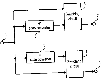
Fig. 1 is a block diagram of a receiver iz~ accordance with a first
exemplary embodiment of the present invention.
Fig. 2 is a block diagram of an i-p scan converter of a receiver in
accordance with a second exemplary embodiment of the present invention.
Fig. 3 explains the operation of the i-p scan converter of the receiver
in accordance with the second exemplary embodiment of the present invention.
Fig. 4 is a block diagram of an i-p scan converter of a receiver in
accordance with a third exemplary embodiment of the present invention.
Fig. 5 explains the operation of the i-p scan converter of the receiver
to in accordance with the third exemplary embodiment of the present invention.
Fig. 6 is a block diagram of a~n i-p scan coztverter of a receiver in
accordance with a fourth exemplary embodiment of the present invention.
Fig. 7 explains the operation of the i-p scaa converter of the receiver
in accordance with the fourth exemplary embodiment o~ the present invention.
Fig. 8 is a block diagram of an i-p scan converter of a receiver in
accordance with a fifth exemplary embodiment of the present invention.
Fig. 9 is a block diagram of a p-i scan converter of a receiver in
accordance with a sixth exemplary embodiment of the present invention.
Fig. 10 is a block diagram of a receiver in accordance with a seventh
zo excrnplary embodiment of the present invention.
Fig. 11 is a block diagram of a selector in a seventh exemplary
embodiment of the present invention.
Fig. 12 explains the operation of a receiver of the prior art.
CA 02230081 1998-02-20
-6
DESCRIPTION OF THE PREFERRED EMBODIMENT
First exem _lary embodiment
A receiver in a first exemplary embodiment of the present invention
is explained with reference to Fig. 1.
The receiver of the first exemplary embodiment comprises a video
signal input terminal 1 which receives the video signal of the interlace
scanning
system (hereafter referred to as the i video signal) or the video signal of
the
progressive scanning system (hereafter referred to as the p video signal), a p
video
signal output terminal 2 for outputting the signal selected by a switching
circuit 6,
to and an i video signal output terminal 3 for outputting the signal selected
by a
switching circuit 7. The receiver is further configured with an i-p scan
converter
4, a p-i scan converter 5, a switching circuit 6, and a switching circuit 7.
The
video signal input to the video signal input terminal 1 is supplied to the i-p
scan
converter 4, p-i scan converter 5, switching circuit 6, acrd switching circuit
7. The
~ s switching circuit 6 also receives the output signal of the i-p scan
converter 4, and
the switching circuit 7 also receives the output signal of the p-i scan
converter 5.
if a television set is designed to be exclusive to the i signal, the
television set is connected to the i video signal output terminal 3 of the
receiver.
On the other hand, a television set designed to be exclusive to the p signal
is
2o connected to the p video signal output terminal 2 of the receiver.
The video signal, encoded by MPEG2, or other format before
transmission, is decoded by a decoder (not illustrated). The decoded video
signal
is input to the video signal input terminal 1 of the receiver. This video
sigmal, as
described above, contains both the i video signal and the p video signal on a
time
25 base.
First, when the i video signal is input, the i-p scan converter 4
CA 02230081 1998-02-20
_7-
converts the i video signal to the p video signal, and outputs the caaverted p
video
signal to the switching circuit 6. The switching circuit 6 selects the
converted p
video signal, and outputs the converted p video signal to the p video signal
output
terminal 2. At this point, the p-i scan converter 5 ceases to operate, and the
switching circuit 7 selects the input video signal from the i video signal
input
terminal 1 to output the i video signal to the i video signal output terminal
3. With
the above operation, video signals in both formats are simultaneously output
from
the respective p video signal output terminal 2 aid i video signal output
terminal
3.
tp For example, signals may be recordable on a VI~S video tape
recorder while being viewed as high picture quality p video signal images by
connecting the p video signal output terminal 2 to a television set designed
to
receive the p video signal, and the i video signal output terminal 3 to a VIiS
video
tape recorder.
t 5 Next, if the p video signal is input to the video signal input terminal
1, the p-i scan converter 5 converts the p signal into the i signal, and
outputs the i
video signal. The switching circuit 7 selects the converted i video signal,
and
outputs the converted i video signal to the i video signal output terminal 3 _
At this
point, the i-p scan converter 4 ceases to operate, and the switching circuit 6
xQ selects the input video image from the video signal input termuoal 1 and
outputs
the p video signal to the p video signal output terminal 2. With the above
operation, video signals in both formats are simultaneously output from the
respective p video signal output terminal 2 and the i video signal output
terminal
3.
zs As explained above, the receiver of this exemplary embodiment, by
providing a switching function, enables the elimination of switching
operations
izrespective of whether a television set which receives broadcast signals
containing
both the i video signal and p video signal is exclusive to the i signal or p
signal.
CA 02230081 1998-02-20
_8_
Second exem 1 embodiment
A block diagram of an i-p scan converter 204 of a receiver in a
second exemplary embodiment of the present invention is explained with
reference
to Figs. 2 and 3. The receiver in the second exemplary embodiment comprises an
s i video signal input terminal 8 for receiving the i video signal, an i
horizontallvertical synchronizing pulse input terminal 9 for receiving the
horizontal synchronizing pulse and vertical synchronizing pulse of the
interlace
scanning system. The receiver also has a p video signal output terminal 10,
and a
p horizontallvertical synchronizing pulse output terminal 11 for outputting
the
t o horizontal synchronizing pulse and vertical. synchronizing pulse of the
progressive
scanning system. This exemplary embodiment employs the i-p scan converter 204
comprising a line memory for time compression 12, a lime memory for delay 13,
a
switching circuit 14, and a double-speed timing generator for progressive
scaxming
signal 15 (hereafter referred to as the p signal double-speed tzncting
generator).
15 A scanning peziod of the p signal is a half (112) the scanning period
of the i signal- Therefore, the i video signal input from the i video signal
input
terminal 8 is input to the line memory for time compression 12. Video data
stored
in the line memory for time compression 12 is compressed by half (1l2) the
time
base for each horizontal scanning period, and output tmhe switching circuit
14.
20 'fhe line memory for delay 13 then receives the output of the line memory
for
time compression 12 which is compressed by half (1.12) the time base, delays
the
line memory output by half (1l2) the horizontal scarring period, and outputs
the
delayed line memory output to the switching circuit 14. Accordingly, the
output
signal of the line memory for time compression 12 and the output signal of the
z5 line memory for delay 12. are shifted by half (112) the horizontal scanning
period
with respect to each other. The switching circuit 14 switches and alternately
outputs these two signals, which are mutually shifted by half (ll2) the
horizontal
scanning period, as required. The p signal is composed in this way to output
CA 02230081 1998-02-20
_g-
composcd p video signal from the p video signal output terminal 10.
The p signal double-speed timing generator 15 generates a p
horiwntal synchronizing pulse and p vertical synchronizing pulse by reducing
the
period of the i horizontal synchronizing pulse and i vertical synchronizing
pulse,
input through the i horizontal/vertical synchronizing input terminal 9, by
half
(ll2).1'he generated signal is output to a timing signal output termite 2~4
for use
as a timing signal in the i-p scan converter. At the same time, the generated
signal
is output to the p hotizontallvertical synchronizing pulse output terminal l
I.
Fig. 3 shows an image of a sct~een when interpolation is executed for
generating the i signal and p signal. In a certain field (n field) of i
signal, the
video signal of one horizontal scanning line of the i signs! is re-scanned
before the
next scanning line of the i signal. lfiis rescanned signal is used as an
interpolation
signal for generating the p signal.
'The second exemplary embodiment thus offers a more inexpensive
receiver employing the i-p scan converter.
Third exem 1 embodiment
A block diagram of an i-p scan converter 304 in a third exemplary
embodiment of the present invention is explained with reference to Figs. 4 and
5.
'fhe receiver of the third exemplary embodiment comprises an a video signal
input
zo terminal 16, i horizontallveztieal synchronizing pulse input terminal 17, p
video
signal output termiztal 18, and p horizontallvertieal synchronizing Pulse
output
terminal 19. This exemplary embodiment employs the i-p scan converter 304
comprising a line memory for interpolation 20, adder 21, divider 22, line
memory
23, line memory 24, switching circuit 25, and p signal double-speed timing
2s generator 26.
The i video signal input from the i video signal input terminal 16 is
CA 02230081 1998-02-20
-la-
input to the line memory for interpolation 20 and also to the adder 21 and the
line
memory 24. The input i video signal is delayed for one horizontal scanning
period
in the line memory for interpolation 20. The adder Z1 adds this delayed video
signal and the original i video signal. The divider ZZ then reduces the output
level
of the adder 21 by half (1/2), and the divided signal is output to the line
memory
23.
This signal stored in the line memory 23 (this is an interpolation
video signal) and the original video signal stored in the line memory 24 are
converted to double speed on the time base, shifted from each other by half
(112)
to the horizontal scanning period, and output to the switching circuit from
respective
line memories 23 and 24. The switching circuit 25 alternately switches and
outputs these two signals to the p video signal output terminal 18. In this
way, the
i video signal is converted to a p video signal.
The p signal double-speed timing generator 26 reduces, by half
t5 (112), the ~riod of the i horizontal synclu'otuzang Pulse and i vertical
synchronizing pulse, input through the i horizontaUvertical synchronizing
poise
iztput terminal 17, to generate the p horizontal synchronizing pulse and P
vertical
synchronizing pulse. The generated synchronizing signal is output to a timing
signs! output terminal 300 for use as a timing signal in the i-p converter. At
the
Zo same tithe, the generated synchronizing signal is output to tt~e p
horizontal/vertical
synchronizing pulse output terminal 19.
Fig_ 5 shows an image of a screen when interpolation is executed for
generating the p signal from the i signal. In a certain field (n field) of the
i signal,
a mcan value of a video signal on a scanning line A and a video signal on a
zs scanning line B is calculated. This calculated value is used as a video
image on a
fme C which is an interpolation line for the p signal.
The third exemplary embodiment thus offers a more inexpensive
CA 02230081 1998-02-20
-11-
receiver employing the i-p scan converter.
Fourth exemplary embodiment
A block diagram of an i-p scan converter 404 of a receiver in
accordance with a fourth exemplary e~oclbodiment of the present invention is
explained with reference to Figs. b and 7. The receiver of the fourth
exemplary
embodiment comprises an i video signal input tenninal 27, i
horizontallvertical
synchronizing pulse input terminal 28, p video signal output terminal 29, and
p
hvrizontallverdcal synchronizing pulse output terminal 30. This exemplary
embodiment employs the i-p scan converter 404 comprising a field memory 31~,
i0 field memory 32, interheld/in-field interpolator 33, movement detector 34,
line
memory 35, line memory 36, switching circuit 37, and p signal. double-speed
riming generator 38 _
fhe i video signal input from tbie i video signal input terminal 27 is
simultaneously supplied to the field memory 31, interfieldlin field
interpolator 33,
i s movement detector 34, and line memory 36. The i video signal is delayed by
one
field in the field memory 31 to create one frame of the p video signal as an
interpolation video signal for the original i video signal. This is shown in
Wig. 7.
In Fig_ 7, an i video signal which is in a position corresponding to
the p sigztal in a field (n+ 1 field) and its previous field (n field), are
extracted as
?o an interpolation signal for creating one fraane of the p video signal.
However, the
about interpolation between fields is effective only in a still picture area
without
any movement.
1n the case of a moving video image, in field interpolation, namely
the averaging process of adjacent scanning lines, as shown in Fig. 5, is
executed.
'1 be movement detector 34 detoets an area of movement by comparing the field
memory 32, the video signal delayed for 2 fields by the field memory 32, and
the
CA 02230081 1998-02-20
-12-
originai i video signal. Based on this movement detection signal, the
interfieldlin-
field intezpolator 33 which receives the original i video signal, the output
signal of
the field memory 31, and the output signal of the field memory 32, executes
interfield interpolation for still pictures, and in-fteld interpolation for
moving
s picture areas.
The line memory 35 which receives the output signal of the
in~erfieldlin-field interpolator 33, the line memory 36 which receives the
original i
video signal, and the switching circuit 37 which switches the output between
the
output of the line memory 35 and the line memory 36, operate in the same way
as
t0 the line memory 23, line memory ?fl, and the switching circuit 25 in Fig. 4
to
output the p video signal to the p video signal output terminal 29. The p
signal
double-speed timing generator 38 receives the i horizontal synchronizing pulse
and
i vertical synchronizing pulse froze the i horizontallverticat synchronizing
pulse
input terminal 28, aad reduces the period of each pulse by half to generate
the p
is horizontal synchronizing pulse and p vertical synchronizing pulse. The
generated
synchronizing signal is output to a timing output terminal 400, and is also
used as
d timing signal in the i-p scan converter. At the same time, the generated
synchronizing signal is output to the p horizontallvertical synchronizing
pulse
output terminal 30.
The receiver, which employs the i-p scan converter in the fourth
exemplary embodiment, reduces the side effect in the secondary exemplary
embodiment, w)aich is that the vertical resolution of still pictures may not
be
unproved by rescanzting the same scanning lane, and that flickering of
scanning
lines is noticeable. The i-p scan converter in this exemplary embodiment may
also
25 improve a remaining problem in the third exemplary embodiment, which is
that
vertical resolution of still pictures znay not be improved by the process of
averaging adjacen~ scanning litres and lower vertical resolution for moving
pictures _
CA 02230081 1998-02-20
-13-
Fifth exemplary embodiment
A block diagram of an i- p scan converter 504 of a receiver in a fifth
exemplary embodiment of the present invention is explained 'with. reference to
Fig.
8. The receiver in the fifth exemplary embodiment comprises an i video signal
input terminal 39, i horizontallvertical synchronizing pulse input terminal
40, p
video signal output terminal 41, and p harizontallvertical synchronizing Pulse
output terminal 42. This exemplary embodiment employs the i-p scan converter
504 comprising an interpolation line memory 43, adder 44, divider 45, Line
memory 46, line memory 47, switching circuit 48, and p signal double-speed
timing gencracor 49.
The receiver in this exemplary embodiment reduces the signal level
of the interpolated video signal tv impmve apparent deterioration in vertical
resolution due to characteristics of display devices, such as CRTs. The
configuration shown in Fig. 8 is basicahy the same as Fig. 4. The difference
is
15 that the divider 45 reduces t~ video signal level within, a range of 0 to
112. Since
the operation of other components are the same as that explained in Fig. 4,
the
explanation is not repeated.
By inserting the divider 45 (which can reduce the video signal level
within a range of 0 to 1l2) in Fig. 8, after the delay line memory 13 in Fig.
2 or
z0 after the line memory 35 in Fig. 6, deterioration of apparent vertical
resolution
can also be improved in the receivers of the second and fourth exemplary
embodiments.
Sixth exe la embodiment
A block diagram of a p-i scan converter of a receiver in a sixth
25 exemplary embodiment of the present invention is explained with reference
to Fig.
9. 'fhe receiver in the sixth exemplary embodiment comprises a p video signal
CA 02230081 1998-02-20
-14-
input terminal 50, p horizoniallvertical synchronizing output terminal 51, i
video
signal output terminal 52, and i lwrizontal/vertical synchronizing pulse
output
terminal 53. lfiis exemplary embodinnent employs the p-i scan converter 605
comprising a line memory for delay 54, adder 55, divider 56, line memory 57,
and timing generator fox interlace scanning signals (i signal timing
generator) 58.
The adder 55 adds the p video signal delayed far one scanning line
in the delay Line memory 54 and the original p video sigmal, and the divider
56
calculates a mean value to g~emte video data for the i signal. The output
signal
of the divider 56 is doubled with respect to a time base in the line memory 57
to
to obtain the i video signal output. The i video signal is output to the i
video signal
outpu~ terminal 52. 'I'he i signal timing generator 58 receives the p
horizontal
synchronising poise and p vertical synchronizing pulse from the p
horizontallvertical synchronizing pulse input ~ernai~nal 51, and doubles their
peritid
to generate the i horizontal synchronizing pulse and i vertical synchronizing
pulse.
The generated synchronizing pulses are output to a timing output terminal
6011,
and used as a timing signal in the p-i convertex. At the same time, the
ge~rated
synchronizing signal is output to the i horizontallvertical synchronizing
Pulse
output terminal 53.
In Fig. 9 line memory for delay 54, adder 55, and divider 56
?0 comprise a low-pass filter between two lines in the vertical direction of
the display
device. if the number o~ the line memory for delay 54 is increased fronn one ~
several, bandwidth charactenstlcs in the vertical direction of the display
device
will become flat and display quality will be improved.
Seventh exem lar ernbod
A block diagram of a receiver in a seventh exemplary embodiment
of the present invention is explained with reference to Figs. 1 U and 11. The
receiver of the seventh exemplary embodiment c~prises the i-p scan converter
4,
CA 02230081 1998-02-20
-15-
p-i scam converter 5, switching circuit 6, switching circuit 7, and a decoder
101.
'rhe dander 101 decodes broadcast signals encoded by MPEG2, for example, and
outputs the i video signal or p video signal in response to the format of the
video
signal in the received broadcast signal. At the sane time, the decoder 101
outputs
ilp identifying information which informs the switching circuits 6 and 7
whether
the format of the received video sig~aal is the i video signal or p video
signal to
control each switching circuit to output its respective signal type. The video
signal
decoded by the decoder 101 is supplied to the i-p scan converter 4, p-i scan
converter 5, switching circuit 6, and switching circuit 7. The signal input to
t1~ i-
p scan converter 4 is scan converted from i to p, and is input to the
switching
circuit 7. The signal input to the p-i scan coaverter 5 is scan converted from
p to
i, and is output to the switching circuit 6.
With the above configuration, the receiver in the seventh exemplary
embodiment identifies the format of the input video signal, and converts
signals in
~ 5 the i-p scan converter 4 or p-i scan converter 5 for outputting:
1) the i signal in an unmodified form from the switching circuit 6,
and the converted p signal from the switching circuit 7, which is converted by
the
i-p converter 4, when the decoder 101 receives the i signal, and
2) the p signal in an unmodified form from the switching circuit 7
zo and the converted i signal from the switching circuit b, which is converted
by the
p-i scan converter 5, when the decoder 101 receives the p signal.
A selector in Fig. 11 may be further Provided downstream of the
process of Fig. 10_ In other words, selectors 102, 103, and 104 have two input
terminals and one output terminal, and the i signal is input to one input
terminal,
zs and the p signal is input to the other input terminal for selecting and
outputting
either the i signal or the p signal. Four or more selectors tray also be
provided In
place of the three selectors shown in Fig. 11.
CA 02230081 1998-02-20
-16-
'This conftguration allows for the independent switching of selectors
102, 103, and 104, when a video image is output to more than one piece of
exteroal equipment, including monitors, television sets, and video tape
recorders.
The output of each selector can be freely deoermined even if each piece of
external
equipment is specific to the i video signal or the p video signal.
Funhermore, by providing the decoder 101 with the function of
detecting which video sigzial can be successfully input to external equipment
connected to the selectors 102, 103, and 104, the output of the selectors 102,
103,
dnd 104 can be switched in response to the detected signal.
t0 In Fig_ 11 above, the 1 signal (composite signal) consisting of
luminance and two color difference signals are assumed to be used as both the
i
input signal and the p input signal. If the component signal is input as the p
signal,
the selectors 102, 103, and 104 may be configured to select the 1 p signal
(two
component signals of luminance and color difference signals) or the 3 i
signals
is (composite)_
With the use of the receiver of the present invention as configured
above, scan conversion of the p signal to an i signal. for receiving mixed
broadcast signals of the p signal and i signal, is automatically implemented
to
allow receiving of broadcastx in more preferred manner.
Zp Specifically, the user may simply desire to connect either the i video
signal output terminal or the p video sigzial output teruunal of the receiver,
depending on the broadcasting format accepted by t~ television set.
'rhe receiver can also be connected to external equipment which can
process only one video signal format without the need for switchover_ This
allows
zs simplification of operation, even when more than two pieces of external
equipment are connected.
CA 02230081 1998-02-20
-i7-
The exemplary embodiments of the present invention are explained
with reference to receiving broadcast signals containing two types of signals,
i.e.,
the i video signal and the p video signal, However, the present invenGton is
not
limited co these two types of signals. For receiving broadcast signals of
three or
more types, for example, tire number of circuit components including scans
conveners, switching circuits, input terminals and output terminals may simply
be
increased as desired. The preferred embodiments described herein are therefore
illustrative and not restrictive. The scope of the invention being indicated
by the
appended claims a>zd all modifications which come within the true spirit of
the
io claims are intended to be embraced tb~erein.