Note: Descriptions are shown in the official language in which they were submitted.
CA 02230420 2000-11-24
- 1 -
PLANAR DIELECTRIC INTEGRATED CIRCUIT
BACKGROUND OF THE INVENTION
1. Field of the Invention
The present invention relates to a planar dielectric
integrated circuit for use in a millimetric-wave band and a
microwave band.
2. Description of the Related Art
In a millimetric-wave band and a microwave band,
transmission lines have been often used which are constructed
by forming a predetermined conductor on a dielectric substrate
of a waveguide, a coaxial line, a microstrip line, a coplanar
line, a slot line, and the like. In particular, in a dielectric
substrate having a transmission line formed thereon, since
connection with electronic components, such as ICs, is easy,
many attempts to form an integrated circuit by mounting
electronic components onto a dielectric substrate have been
made.
However, in the conventional microstrip line, coplanar
line, slot line, and the like, since transmission loss is
relatively large, these are not suitable for a circuit requiring,
particularly, a low transmission loss. Therefore, the
CA 02230420 2000-11-24
applicant of the present invention submitted the invention
concerning a planar dielectric line and an integrated circuit,
which solve these problems, in Japanese laid-open Patent
Application No. Hei-08-265007.
Meanwhile, since t;he input/output section of electronic
components, such as semiconductor devices, and the planar
dielectric line generally differ in the electromagnetic-field
distribution, merely mounting electronic components to the
planar dielectric line causes the conversion loss to increase
greatly. Further, if electronic components are only mounted
to one surface of the dielectric plate, connection between the
electromagnetic field on the back surface thereof and the
electronic components is not made, this point also leading to
an increase in the conversion loss. Mounting electronic
components to both surfaces of the dielectric plate eliminates
the latter problem; however, this results in a decrease in the
characteristic reproducibility (yield) due to the
characteristic variations of the electronic components, an
increase in loss, and an increase in the material and mounting
costs.
SUMMARY OF THE INVENTION
CA 02230420 2000-11-24
- 3 -
An object of the present invention is to provide a planar
dielectric integrated circuit such that energy conversion loss
between the planar dielectric line and electronic components
is small, and impedance matching between them is obtained
easily.
According to the aspect of the present invention, to
perform integration by reducing a signal loss~in the coupled
section of the planar dielectric line and the electronic
components and while maintaining a low loss characteristic,
which is a feature of the planar dielectric line, a planar
dielectric line is constructed such that two conductors are
provided at a fixed distance on a first main surface of a
dielectric plate to provide a first slot, two conductors are
provided at a fixed distance on a second main surface of a
dielectric plate to pravide a second slot which opposes the
first slot, with the area sandwiched between the first slot
and the second slot of the dielectric plate being formed as
a plane-wave propagation area. A coplanar line is provided in
the end portion or at the midpoint of the planar dielectric
line, a line-conversion conductor pattern is provided which
projects from the center conductor of the coplanar line in a
direction at right angles to the planar dielectric line, and
CA 02230420 2000-11-24
- 4 -
electronic components are disposed in such a manner as to be
extended over the slot line.
With this construction, an LSM-mode signal which
propagates through the planar dielectric line is coupled to
the line-conversion conductor pattern which projects in a
direction at right angles to the planar dielectric line, and
is converted into the propagation mode of the coplanar line.
And a signal is input to the electronic components disposed
in such a manner as to extend over this coplanar line.
Conversely, when a signal is output from the electronic
components, the signal is propagated in the propagation mode
of the coplanar line and, as a result of the coupling between
the line-conversion conductor pattern which projects in a
direction at right angles to the planar dielectric line and
the planar dielectric line, the signal propagate through the
planar dielectric line in the LSM mode.
Preferably, two planar dielectric lines are constructed
such that a first slot is provided by disposing two electrodes
at ffixed intervals on a ffirst main surface of the dielectric
plate, a second slot, which opposes the first slot, is provided
by disposing two electrodes at fixed intervals on a second main
surface of the dielectric plate, with the area sandwiched by
CA 02230420 2000-11-24
- 5 -
the first slot and the second slot of the conductor plate being
formed as a propagation area of a plane wave. A first
line-conversion conductor pattern which is connected to the
electromagnetic field of the slot line and the first planar
dielectric line is provided at one end portion of the slot line,
and a coplanar line is provided in the vicinity of the other
end portion of the slot line. A second line-conversion
conductor pattern is provided which projects from the center
conductor at the end portion of the coplanar line in a direction
at right angles to the planar dielectric line. The electronic
components are disposed in such a manner as to extend over the
coplanar line and the slot line.
With this construction, the LSM-mode signal which
propagates through the first planar dielectric line is coupled
to the first line-conversion conductor pattern, is converted
into a TE mode, propagates through the slot line, and is input
to the electronic components. The LSM-mode signal which
propagates through the second planar dielectric line is coupled
to the second line-conversion conductor pattern, is converted
into the propagation mode of the coplanar line, and is input
to the electronic component. In response, the electronic
component performs a signal processing, such as synthesizing
CA 02230420 2000-11-24
_ 5 _
two signals input from the first and second planar dielectric
lines . When, for example, this electronic component is a mixer
FET (field-effect transistor) or a mixer diode, by inputting
an RF signal and a Lo signal from the first and second planar
dielectric lines, respectively, an IF signal can be taken from
the bias voltage supply line to the external source.
' Preferably, a short stub which is used to obtain impedance
matching between the line-conversion conductor pattern and the
electronic components is provided at the midpoint of the slot
line or the coplanar line. As a result, impedance matching is
obtained between the line-conversion conductor pattern and the
electronic components, and the loss in the connection section
of the slot line and the electronic components is reduced.
Further, preferably, an impedance matching circuit is
provided between the line-conversion conductor pattern and the
slot line or the coplanar line. As a result, impedance matching
is obtained between the line-conversion conductor pattern and
the planar dielectric :Line and the slot line or the coplanar
line, thereby suppressing unwanted reflection and reducing the
transmission loss caused by line conversion.
The above and further objects, aspects and novel features
of the invention will become more apparent from the following
CA 02230420 2000-11-24
_ 7 _
detailed description when read in connection with the
accompanying drawings.
BRIEF DESCRIPTION OF THE DRAWINGS
Figs. lA and 1H are partial, exploded perspective views
showing the construction of a mixer according to a first
embodiment of the present invention.
Fig. 2 is a perspective view showing the entire
construction of the mixer.
Fig. 3 is a sectional view of a planar dielectric line.
Fig. 4 is a sectional view of the planar dielectric line.
Fig. 5 is a view shawing conductor patterns on a circuit
substrate.
Fig. 6 is a view showing a state in which an FET is mounted
with respect to Fig. 5.
Fig. 7 is a view showing the construction of an
interdigital capacitor.
Fig. 8 is a view showing the construction of the main
portion of a mixer according to a second embodiment of the
present invention.
Fig. 9 is an exploded perspective view of a multiplier
according to a third embodiment of the present invention.
CA 02230420 2000-11-24
- 8 -
DESCRIPTION OF THE PREFERRED EMBODIMENTS
The construction of a mixer according to a first embodiment
of the present invention will be described with reference to
Figs. lA and 1H to 7.
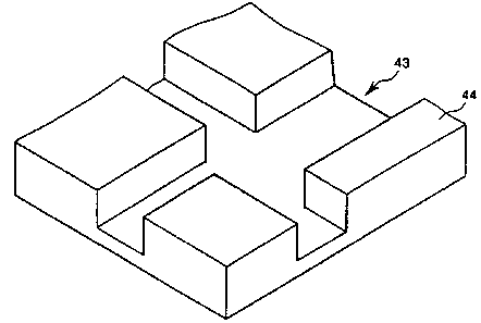
Figs. lA and 1B are partial, exploded perspective views
showing the construction of the mixer. Fig. lA is a perspective
view of a low-part conductor plate, with a groove being formed
in the top surface of the low-part conductor plate in the figure,
thereby a space section indicated by 43 being provided. Fig.
1B shows a state in which a circuit substrate 30 is placed on
the top surface of the low-part conductor plate shown in Fig.
lA. The circuit substrate 30 is such that various conductor
patterns are formed on the top and bottom surfaces of the
conductor plate, with a slot-line-input-type FET
(milli.metric-wave GaAs FET) 50 being mounted onto the top
surface of the circuit substrate 30. Reference numerals 14 and
24 each denote a slot on the top surface of the circuit substrate
30, formed by exposing the upper surface of the substrate 30,
and, as will be described later, form first and second planar
dielectric lines together with the opposing slot on the bottom
surface with the circuit substrate 30 interposed in between.
CA 02230420 2000-11-24
- 9 -
Reference numeral 12 denotes a slot line formed at the end
portion of the first planar dielectric line. Reference numeral
denotes a first line-conversion conductor pattern provided
at one end portion of the slot line 12, which is connected to
the first planar dielectric line and which is used to perform
mode conversion between it and the slot line. Reference
numeral 16 denotes a coplanar line formed in the vicinity of
the other end portion of the slot line 12, with a second
line-conversion conductor pattern 17 projecting from the
center conductor of the coplanar line in a direction at right
angles to the second planar dielectric line. Reference
numerals 31 and 32 each denote a coplanar line, which supplies
a gate bias voltage and a drain bias voltage to an FET 50. These
two coplanar lines 31 and 32 are provided with filters indicated
by F. Reference numeral 18 denotes an interdigital capacitor,
forming a capacitor between the center conductor of the coplanar
line 31 and another conductor. The peripheral portion of each
of the above-described patterns covers, as an RF-GND ( grounding
conductor) , the top surface of the circuit substrate 30. Slots
which oppose the slots 14 and 24, respectively, are provided
on the bottom surface of the circuit substrate 30, and in the
other area of the bottom surface of the circuit substrate 30,
CA 02230420 2000-11-24
- 10 -
an RF-GND is formed.
Fig. 2 shows a state in which an upper-part conductor plate
41 is further placed on the top surface with respect to the
state shown in Fig. 1B. By forming a groove in a plane symmetry
(mirror symmetry) with respect to the groove of the low-part
conductor plate 44 in the inner surface of the upper-part
conductor plate 41, a space section 42 is provided.
Fig. 3 is a sectional view passing through a slot 24 shown
in Fig. 1. In Fig. 3, reference numeral 23 denotes a conductor
plate, with two conductor plates 21a and 21b being formed on
the first main surface (the top surface in the figure) thereof,
forming the portion indicated by 24 as a first slot. Further,
two conductor plates 22a and 22b are formed on the second main
surface (the bottom surface in the figure) of the conductor
plate 23, forming the portion indicated by 25 as a second slot.
The two conductor plates 41 and 44 are provided with spaces
42 and 43 near slots 24 and 25, and cause both the section between
the conductor plates 21a and 21b and the section between the
conductor plates 22a and 22b to conduct.
The portion indicated by 23c, shown in Fig. 3, which is
provided in the conductor plate 23 between the opposing slots
24 and 25, becomes a propagation area in which a high-frequency
CA 02230420 2000-11-24
- 11 -
signal having a desired propagation frequency fb is made to
propagate. Further, the portions indicated by 23a and 23b on
both sides, which sandwich the propagation area 23c, become
cut-off areas.
Fig. 4 is a sectional view in a plane in which the
propagation area of the planar dielectric line shown in Fig.
3 passes in the direction of the propagation. As shown in Fig.
4, a plane electromagnetic wave pw23, which is an
electromagnetic wave of a plane wave, enters the top surface
(the slot 24 portion) of the conductor plate 23 at a
predetermined incidence angle 8 and is reflected at a reflection
angle 8 equal to the incidence angle 8. Further, the plane
electromagnetic wave pw23 reflected on the top surface of the
conductor plate 23 enters the bottom surface (the slot 25
portion) of the conductor plate 23 at an incidence angle 8 and
is reflected at a reflection angle 8 equal to the incidence
angle 8. Thereafter, the plane electromagnetic wave pw23 is
repeatedly reflected alternately with the surfaces of the slots
24 and 25 portions of the canductor plate 23 as the boundary
surfaces, and propagates through the propagation area 23c of
the conductor plate 23 in the TE mode. In other words, the
specific dielectric constant of the conductor plate 23 and the
CA 02230420 2000-11-24
- 12 -
thickness t23 of the conductor plate 23 are determined so that
the desired propagation frequency fb becomes equal to or greater
than a critical frequency fda ( the frequency at which a state
is reached in which the incidence angle 8 is decreased, the
plane electromagnetic wave pw23 passes through the spaces 42
and 43, and the plane electromagnetic wave pw23 which propagates
through the propagation area 23c is attenuated).
Opposing electrodes 21a and 22a with the conductor plate
23, shown in Fig. 3, interposed therebetween form a
parallel-plate waveguide having a cut-off frequency
sufficiently higher than the desired propagation frequency fb
with respect to the TE wave. As a result, a cut-off area 23a
with respect to the TE wave having electric-field components
parallel to the electrodes 21a and 22a is formed on one side
in the width direction of the conductor plate 23 sandwiched
by the electrodes 21a and 22a. In a similar manner, electrodes
21b and 22b with the conductor plate 23 interposed therebetween
form a parallel-plate waveguide having a cut-off frequency
sufficiently higher than the desired propagation frequency fb
with respect to the TE wave, and a cut-off area 23b with respect
to the TE wave is formed on one side in the width direction
of the conductor plate 23 sandwiched by the electrodes 21a and
CA 02230420 2000-11-24
-- 13 -
22b.
Further, the top surface of the space 42 in the figure
and the electrode 21a form a parallel-plate waveguide, and the
thickness t42 thereof is set so that the cut-off frequency with
respect to the TE wave of the parallel-plate waveguide becomes
sufficiently higher than the desired propagation frequency fb.
As a result, a cut-off area with respect to the TE wave is
formed in the portion indicated by 42a. In a similar manner,
a cut-off area with respect to the TE wave is formed in each
of the portions indicated by 42b, 43a, and 43b.
The opposing inner surface ( the longitudinal wall in the
figure) of the space 42 forms a parallel-plate waveguide, and
the width W2 thereof is set so that the cut-off frequency with
respect to the TE wave of the parallel-plate waveguide becomes
sufficiently higher than the desired propagationfrequencyfb,
thereby forming a cut-off area 42d. For the space 43, similarly,
a cut-off area 43d is formed.
As a result of forming the planar dielectric line as
described above, it is possible to cause the
electromagnetic-field energy of a high-frequencysignal having
a frequency equal to or higher than the critical frequency fda
to be concentrated in the inside of the propagation area 23c
CA 02230420 2000-11-24
- 14 -
and in the vicinity thereof and to cause the plane wave to
propagate in the direction of the length ( in the direction of
the z axis) of the conductor plate 23.
In the case where a signal of, for example, a 60-GHz band
is propagated, if the specific dielectric constant of the
conductor plate 23 is set at 20 to 30, and the plate thickness
t at 0.3 to 0.8 Vim, an appropriate line width W1 is 0.4 to 1.6
mm, and a characteristic impedance in a range of 30 to 200 ~
is obtained. Further, if a conductor plate having a specific
dielectric constant of 20 or more is used as described above,
energy of 90% or more is trapped within the conductor plate,
and a transmission line with a very low loss because of total
reflection can be realized.
In the above, the second planar dielectric line is
described. The first planar dielectric line, including the
slot 14 shown in Fig. 1, is similarly constructed.
Fig. 5 is a view showing the conductor patterns of the
main portion of the top surface of the circuit substrate 30.
In Fig. 5, reference numeral 12 denotes a slot line, with a
first line-conversion conductor pattern 10 being formed at one
end portion of this slot line 12. This first line-conversion
conductor pattern 10 is in the shape of a dipole antenna, as
CA 02230420 2000-11-24
- 15 -
indicated by l0a and lOb, respectively. The root portion of
the line-conversion conductor pattern 10 with respect to the
end portion of the slot line 12 form an impedance matching
section (impedance matching circuit) R which is tapered
moderately from the slot line 12 toward the line-conversion
conductor pattern 10 in order that the wiring resistance of
the line-conversion conductor pattern 10 is reduced to decrease
the conversion loss . If the wavelength of the frequency in the
used frequency band in each of the electrode patterns l0a and
lOb and the impedance matching section R is denoted as ~1, they
have a length of nearly .1/4, and the width of the slot line
12 is determined by the characteristic impedance of the line
to be designed. A line-conversion conductor pattern having
same structure is explained in the co-pending U.S. patent
application No. (our case:5100020). For example, a
characteristic impedance of 30 to 100 ~ can be realized at a
width of 0.05 to 0.20 mm. A coplanar line 16 is formed by an
RF-GND and a center conductor 38, with the second line-
conversion conductor pattern I7 being projected from this
center conductor 38 in a direction at right angles to the second
planar dielectric line, including a slot 24. This second
line-conversion conductor pattern forms the shape of a monopole
CA 02230420 2000-11-24
- 16 -
antenna. The dimensions of the coplanar line 16 are determined
by the characteristic impedance of the line to be designed.
For example, when the width of the center conductor is 0.1
to 0.15 mm and the spacing of the RF-GNDs on both sides thereof
is 0.2 to 1.0 mm, a characteristic impedance of 30 to 90 ~ can
be realized. As a result of the above, this coplanar line 16
forms an impedance matching circuit, as a pattern which is
tapered up to a fixed width from the root portion thereof in
the direction of the end (the second line-conversion conductor
pattern 17). As described above, the characteristic impedance
of the planar dielectric line is 30 to 200 ~, and the
input/output impedance of the FET (millimetric-wave GaAs FET)
50 is usually about 30 to 90 ~2; therefore, the four, including
the planar dielectric line, the slot line, the FET, and the
coplanar line, easily obtain impedance matching. Further, by
providing a short stub S having an appropriate length at the
midpoint of the slot line 12, it is possible to obtain impedance
matching easily between the first line-conversion conductor
pattern 10 and the FET. In a similar manner, by providing an
open stub at the midpoint of the coplanar line 16, it is possible
to obtain impedance matching easily between the second
line-conversion conductor pattern 17 and the FET.
CA 02230420 2000-11-24
- 17 -
In Fig. 5, reference numeral 37 denotes a conductor for
branching the slot line, reference numeral 38 denotes a center
conductor of the coplanar line 16, reference numeral 35 denotes
a gate terminal, and reference numeral 36 denotes a drain
terminal, to which is connected each terminal of the FET to
be described later. Reference numerals 31 and 32 each denote
a coplanar line, with the center conductors 33 and 34 thereof
being extended out to the gate terminal 35 and the drain terminal
36, respectively. As also shown in Fig. 1B, filters which
function as low-pass filters indicated by F are fornted at the
midpoint of the coplanar lines 31 and 32 so that the RF signal
does not leak to the bias circuit side and does not propagate.
Between the two planar dielectric lines, an RF-GND is
provided, and a distance is required such that an RF signal
or a Lo signal is cut off between the two planar dielectric
lines; a width equal to or greater than 1 mm is sufficient.
Fig. 6 is a view showing a state in which the FET 50 is
mounted with respect to the state shown in Fig. 5. In Fig.
6, reference numerals 5:L and 52 denote the source terminals
of the FET 50, reference numeral 53 denotes a gate terminal,
and reference numeral 54 denotes a drain terminal. The
portions indicated by 55 and 56 are active areas; a field-
CA 02230420 2000-11-24
- 18
effect transistor is formed in each of these portions, and the
source terminals 51 and 52, the gate terminal 53, and the drain
terminal 54 are each extended out. Between the source
terminals 51 and 51, and the gate terminal 53 and the drain
terminal 54, and between the gate terminal 53 and the drain
terminal 54, and the source terminals 52 and 52, a slot line
is formed, as shown in the figure. The cross-hatched portion
is a viahole formation portion, and each terminal extends out
to the back-surface side of the chip.
The arrows in the figure show the electric-field
distribution of a signal which propagates through the slot line
12 and the coplanar line 16.. The RF signal of the LSM mode,
which propagates from top to bottom in the figure through the
first planar dielectric line including the slot indicated by
14 in the figure, is converted into a mode (TE mode) of the
slot line via the first line-conversion conductor pattern 10,
and this TE-mode signal propagates through the slot line 12
and is applied, as a voltage signal, between the source and
the gate of the FET 50. Meanwhile, the Lo signal of the LSM
mode, which propagates from right to left in the figure through
the second planar dielectric line including the slot indicated
by 24, is coupled to the second line-conversion conductor
CA 02230420 2000-11-24
- 19 -
pattern 17, is converted into the mode of the coplanar line,
propagates through the coplanar line 16, and is applied, as
a voltage signal, between the source and the gate via the slot
line of the FET 50. Here, if a gate bias voltage and a drain
bias voltage are applied via the center conductors 33 and 34
of the coplanar lines 31 and 32, respectively, frequency
components (IF signal) between the RF signal and the Lo signal
are generated by a non-linear parameter, such as mutual
conductance of the FET. In that case, the RF signal is input
at an opposite phase to the two FETs and the Lo signal is input
at the same phase thereto, functioning as a balance-type mixer.
Normally, when a balance-type mixer is constructed, since an
opposite-phase waveform is generated, a circuit, such as a phase
shifter, must be added. However, according to this embodiment,
a special phase shifter is not required, and the circuit is
formed into a small size.
Although in the example shown in Fig. 6 the chip is mounted
in such a way that the surface on which the semiconductor devices
are formed becomes the top surface, the chip may be mounted
in such a way that the surface on which the semiconductor devices
are formed faces downwards, and the circuit substrate 30 and
the slot line of the FET are directly bump-connected. In this
CA 02230420 2000-11-24
- 20 -
case, the slot line of the FET must be spaced apart from the
dielectric plate by more than some tens of ~m in order to prevent
parasitic coupling with the dielectric plate, and a high degree
of bump connection technology is required. However, since
viaholes are not necessary, the construction of the FET can
be simplified.
Further, in the example shown in Fig. 6, the RF signal
is input from the first planar dielectric line and the Lo signal
is input from the second planar dielectric line. However, if,
conversely, the RF signal is input from the second planar
dielectric line and the Lo signal is input from the first planar
dielectric line, in a similar manner, this functions as a
balance-type mixer.
Fig. 7 is a view showing the construction of an
interdigital capacitor 18 shown in Fig. 1 . In Fig. 7, reference
numerals 19 and 19' each denote a coplanar line, with the center
conductor of the coplanar line 19 branching from the center
conductor of the coplanar line 31. The interdigital capacitor
18, which is used to generate capacitance between the center
conductors of the coplanar line 19 and 19°, forms an
interdigital-type conductor pattern. In this embodiment,
since the interdigital-type conductor pattern is formed in a
CA 02230420 2000-11-24
- 21 -
dielectric plate with a high dielectric constant, a capacitor
having a relatively large capacitance of 10 pF or more can be
easily realized. In the coplanar line 31 , by making the forward
portion from the branching point of the coplanar line 19 have
a high impedance, the leakage of the IF signal to the bias
voltage supply circuit side is prevented.
As stated above, since in this high-frequency amplifier
a planar dielectric line having a large effect of trapping a
propagation electromagnetic field is used for input and output,
parasitic coupling between this circuit and external circuits
can be prevented. Further, since Q of the planar dielectric
line is high (in the above-described example, Q>500), it is
possible to minimize the transmission loss. Further, since the
electrode patterns on the circuit substrate can be produced
by using technology similar to a conventional circuit-
substrate manufacturing technology using photolithography,
the~electrode patterns can be manufactured very easily and at
a low cost.
Next, the construction of the main portion of a mixer
according to a second embodiment of the present invention will
be described with reference to Fig. 8. Although in the example
shown in Fig. 6 an FET is used, in this second embodiment, a
CA 02230420 2000-11-24
- 22 -
mixer diode is used. Fig. 8 shows the mounting portion of the
mixer diode. In Fig. 8, reference numeral 150 denotes a mixer
diode, reference numeral 151 denotes a cathode terminal,
reference numeral 152 denotes an anode terminal, and reference
numeral 153 denotes a cathode/anode terminal. The portions
indicated by 155 and 156 are active areas, each of which form
a diode. Between the cathode terminals 151 and 151, and the
cathode/anode terminals 153 and 153, and between the
cathode/anode terminals 153 and 153, and the anode terminals
152 and 152, a slot line is formed as shown in the figure. The
cross-hatched portion is a viahole formation portion, and each
terminal extends out to the back-surface side of the chip.
The arrows in the figure show the electric-field
distribution of a signal which propagates through the slot line
12 and the coplanar line 16. The RF signal of the slot-line
mode, which propagates from left to right in the figure, is
made to branch at a conductor 137 for branching a slot line,
and is applied, as a voltage signal, between the anode and the
cathode of each of the two diodes of the mixer diode 150.
Meanwhile, the Lo signal of the coplanar line mode, which
propagates from right to left in the figure, is applied, as
a voltage signal, between the anode and the cathode. Here, if
CA 02230420 2000-11-24
- 23 -
a bias voltage is applied between the anode and the cathode
of each of the two diodes via the center conductor of the
coplanar line 31, frequency components ( IF signal ) between the
RF signal and the Lo signal are generated by a non-linear
parameter of the diode. In that case, the RF signal is input
at an opposite phase to the two diodes and the Lo signal is
input at the same phase thereto, functioning as a balance-
type mixer. Also in this case, in the same way as in the first
embodiment, a small balance-type mixer can be constructed
without adding a circuit, such as a phase shifter.
Incidentally, although the mixer using the FET as in the
first embodiment makes it possible to reduce the conversion
loss to a range of 0 to 4 dB by using the amplification function
of the FET, the NF characteristic is generally deteriorated
to 10 dH or more. If the diode is used as in this second
embodiment, the conversion loss is as large as 5 to 8 dB or
more; however, an NF characteristic of equal to or less than
6 dH can be obtained. Further, there is the advantage that the
power consumption is small.
In the example shown in Fig. 8, the RF signal is input
from the slot line and the Lo signal is input from the coplanar
line. However, even if, conversely, the RF signal is input from
CA 02230420 2000-11-24
- 24 -
the coplanar line and the Lo signal is input from the slot line,
in a similar manner, this functions as a balance-type mixer.
Next, the construction of a multiplier (a second
harmonic-wave generator) according to a third embodiment of
the present invention will be described with reference to Fig.
9.
Fig. 9 is a perspective view in a state (the upper-part
conductor plate is removed) in which the circuit substrate 30
is placed on the low-part conductor plate 44. This multiplier
is, from a construction viewpoint, such that basically, the
interdigital capacitor :18 is removed from the mixer shown in
Fig. 1H. Therefore, in the low-part conductor plate 44 and the
upper-part conductor plate of this multiplier, grooves for
providing a space in the periphery of the interdigital capacitor
18 shown in Fig. 1B and the coplanar line which is connected
thereto are not formed.
In the construction shown in Fig. 9, the input signal,
which is propagated from the first planar dielectric line
including the slot 14, is coupled to the first line-conversion
conductor pattern 10, is converted into the mode of the slot
line, and is input between the gate and the source of the FET
0
50 of a slot-line input structure at a phase difference of 180
CA 02230420 2000-11-24
- 25 -
due to the division of the slot line 12. In this FET 50, a bias
voltage is applied in the vicinity of a threshold value at which
harmonic waves are generated strongly, and a fundamental wave
and a second harmonic wave from among the generated harmonic
waves are output from between the drain and the source of the
FET. At this time, since the fundamental wave is out of phase
c
by 18a in the same manner as on the input side, the fundamental
wave propagates through the coplanar line 16 in the slot mode
as is, but since the phases of the the second harmonic waves
coincide with each other (the phase difference is 0.q), the
second harmonic wave propagates through the coplanar line 16
in the coplanar mode. In the mode conversion portion between
the second planar dielectric line including a slot 24, and the
coplanar line 16, the second line-conversion conductor pattern
17 which projects from the center conductor of the coplanar
line 16 and the second planar dielectric line are coupled to
each other, and mode conversion is performed. However, since
the fundamental wave is out of phase, this is reflected without
being converted. Therefore, only the second harmonic wave is
output to the second planar dielectric line so that the leakage
of the fundamental wave to the output side is prevented. For
example, by inputting a signal of 30 GHz from the first planar
MUR.ATA T90164VO.DOC.
CA 02230420 2000-11-24
- 26 -
dielectric line, it is possible to output only the desired
60-GHz signal from the second planar dielectric line.
In this way, a small balance-type multiplier which does
not leak a fundamental wave can be easily constructed by the
converter between the planar dielectri c line and the slot line,
and the converter between the planar dielectric line and the
coplanar line. In the connection joint of the second planar
dielectric line and the coplanar line 16, if the electrodes
on both sides of the coplanar line 16 are connected by a wire
30 shown in the figure or if these are connected by the
conductors of multilaye.red wiring, the fundamental wave can
be suppressed more reliably.
Although in each embodiment a planar dielectric
integrated circuit using two of the first and second line-
conversion conductor patterns is described as an example,
similarly, by providing a coplanar line at the end portion or
at the midpoint of the planar dielectric line and by providing
only one line-conversion conductor pattern which projects from
the center conductor of the coplanar line in a direction at
right angles to the planar dielectric line, it is possible to
construct an integrated circuit of a planar dielectric line
and electronic components. Further, by providing a coplanar
CA 02230420 2000-11-24
_ 27 _
line at the end portion or at the midpoint of each of the two
planar dielectric lines and by providing two monopole-type
line-conversion conductor patterns which project from the
center conductors of the two coplanar lines in a direction at
right angles to the respective planar dielectric lines, it is
possible to construct an integrated circuit of the two planar
dielectric lines and the electronic components.. According to
the latter construction, it becomes possible to perform signal
processing, such as amplification, on a signal which enters
from one planar dielectric line and to output the signal to
the other planar dielectric line.
According to the invention since the space
between the planar dielectric line and the electronic
components is connected via the line-conversion conductor
pattern and the coplanar line, it is possible to perform
integration by reducing the signal loss in the connection
section of the planar dielectric line and the electronic
components and while maintaining a low loss characteristic,
which is a feature of the planar dielectric line.
According to the invention , Since two signals
which propagate through the first and second planar dielectric
lines are input to the electronic components in each of the
CA 02230420 2000-11-24
_ 28 _
slot line mode and the coplanar line mode, it is possible to
construct easily an integrated circuit which performs signal
processing, such as synthesizing two signals, using electronic
components . In the case where, for example, this electronic
component is a mixer FET or a mixer diode, by inputting an RF
signal and a Lo signal :from the first and second planar
dielectric lines, respectively, a balance-type mixer is
constructed, and an IF signal can be taken from the bias voltage
supply line to the external source.
According to the invention impedance matching
is obtained between the line-conversion conductor pattern and
the electronic components, and the loss in the connection
section of the slot line or the coplanar line, and the electronic
components is reduced.
According to the invention impedance matching
is obtained between the line-conversion conductor pattern and
the slot line or the coplanar line, thereby suppressing unwanted
reflection and reducing the transmission loss caused by line
conversion.
Many different embodiments of the present invention may
be constructed without departing from the spirit and scope of
the present invention. It should be understood that the
CA 02230420 2000-11-24
- 29 -
present invention is not limited to the specific embodiments
described in this specification. To the contrary, the present
invention is intended to cover various modifications and
equivalent arrangements included within the spirit and scope
of the invention as hereafter claimed. The scope of the
following claims is to be accorded the broadest interpretation
so as to encompass all such modifications, equivalent
structures and functions.