Note: Descriptions are shown in the official language in which they were submitted.
CA 02230481 1998-04-01
-
METHOD AND DEVICE FOR TIIE AGGREGATION
OF SIGNALS FROM SAMPLING VALUES
Field of the Invention
The invention concerns a method and a device for
aggregating N ~ 1 band-limited time signals with a
bandwidth of 5 B each, which are present as analog and/or
digital sampling values and have a respective sampling
frequency of fA > 2B. Such a method is known from DE 32
00 934 A1.
Descri~tion of the Prior Art
An aggregation of analog signals by means of
adders is described for example in the textbook
"Semiconductor circuit technology" by Tietze and Schenk,
8th. edition, 1986, pages 299 and 300 as well as 579 to
581.
The aggregation of digital signals from analog
input signals with an intermediate analog-digital
converter (ADC) via a digital signal processor (DSP), and
a reanalogation of the processed signals by means of a
digital-analog converter (DAC), particularly in the area
of video signals, is described for example in EP 0 695
066 A2.
A linear aggregation of several band-limited time
signals into a new composite signal takes place among
other things in audio technology, where audio signals are
superimposed by mixing the sounds from several different
sources, or in video technology where video signals are
combined into a new video signal by cross-fading the
images from two different sources. The areas of
application for sound mixing are for example in radio, in
the disk recording industry and in the production of
other sound carriers. Furthermore, sound mixing is
required for audio conference circuits, i.e. for the
aggregation of several sound signals from different
CA 02230481 1998-04-01
-
sources in the area of te]ecommunications. A mixing of
images by cross-fading several video signals is usual for
example in television, in the production of video disks
and video displays on other video carriers, video
recorders, camcorders and such. Although no video mixing
takes place in video conferences, windows are faded into
a joint video for the different participants in the
conference system.
With the method for mixing low frequency signals
known from the DE 32 00 934 A1 cited in the beginning,
which are present in the form of digital scanning
samples, the pulses intended for the common terminal,
which must be rendered jointly audible in the respective
terminal, are aggregated by an analog adder and are
transmitted within one time frame in the form of an
aggregate pulse which controls the terminal during the
entire time frame.
A disadvantage of the known methods is the
relatively long calculation time for the aggregation of
the individual signals by a digital computer, or by a
hardware circuit of adding units. In addition there is
considerable damping of the signals and thus a loss of
information when converting from analog to digital
signals and vice versa during the reanalogation of the
added signals in the case of a digital aggregation.
Summary of the Invention
The object of the present invention is therefore
to improve a method of the kind cited in the beginning in
a way so that the aggregation can be carried out in a
considerably shorter calculation time, so that possibly a
number of slow and expensive adder elements can be saved,
and minimizing the damping of the signals during the
CA 02230481 1998-04-01
processing and thus the corresponding loss of
information.
The invention achieves this object in as
surprising as well as an effective a manner in that the
sampling values of all N time signals are offset in time
and superimposed on each other, and are jointly input to
a low-pass filter with a bandwidth of B' > B, and that a
composite signal is tapped off from the output of the
low-pass filter.
In contrast to the known methods, in which signals
from different sources that are present as analog or
digital sampling values are converted separately for each
signal into analog signals, which are aggregated by means
of one or several analog adders or by a digital
processor, in the method of the invention the sampling
values of different time signals are offset in time and
superimposed on each other, and converted to analog by
means of a passive low-pass filter. The sampling values
of different signals, each of which was sampled at a
frequency fA, are combined by means of a time-division
multiplex method into a superimposed signal with the
frequency of N ~ fA. During the subsequent filtration
with a low-pass filter of the bandwidth B' = fA/2, an
analog composite signal is generated, which can be
sampled for further processing at the frequency of fA.
One the one hand this results in a qualitatively
better and faster aggregation, on the other the
aggregation can be achieved in a more cost-effective
manner due to the saving of an adder unit or a
corresponding processor for the digital aggregation of
the input signals. Another advantage is that a device
which is suitable for carrying out the method of the
CA 02230481 1998-04-01
invention can be integrated in a simple manner into an
integrated switching circuit, for example a VLSI chip.
On the other hand the method of the invention can easily
be built into a DSP software, with the corresponding gain
in calculation time. The method of the invention is
suitable for adding both digital as well as analog input
values.
Particularly preferred is a configuration of the
method of the invention in which the sampling values of
the N time signals are offset from each other
equidistantly in time. This allows from the outset to
establish a rigid and always known time-relation of the
signals from different sources, which remains the same.
Another preferred configuration of the invention
provides for the sampling values, which are offset in
time with respect to each other, to be input into the
low-pass filter at a clock frequency of N fA.
When analog sampling values are input in another
advantageous configuration of the invention, an analog
low-pass filter can be used, whose output has a time-
continuous composite signal and causes the formation of a
perfect aggregation of the partial signals.
Preferably this method is developed further in
that analog sampling values are obtained by sampling the
time-continuous composite signal.
As an alternative, other configurations into which
digital sampling values are input provide for the use of
a digital low-pass filter which operates at the clock
frequency of n ~ fA, whose output has a composite signal
with n fA sampling values per unit, i.e. in oversampled
CA 02230481 1998-04-01
form. This allows to utilize all the advantages of an
oversampling method.
A further development of this configuration
provides for the oversampled composite signal to be input
into a digital-analog (D/A) converter which operates at
the clock frequency of N ~ fA, and whose output signal
produces the time-continuo-us composite signal via
subsequent filtration, preferably by means of a resistor-
capacitor (RC) element. Instead of the expensive filter
installation, a very simple cost-effective RC filter
element can be used which, because of the oversampling,
ensures sufficient suppression of the mirror signals that
periodically occur in the frequency space in accordance
with a Fourier transformation.
A further development is particularly
advantageous, whereby the oversampled composite signal
is transferred to a lower sampling frequency i fA c N
fA, where preferably i = 1, by periodically omitting
sampling values (= decimation). Inversely, a higher
sampling frequency can also be achieved by means of
sampling rate conversion, by introducing fictitious
sampling values "0" in intermediate areas, where low-pass
filtration produces a perfect total signal at the end.
The method of the invention can be carried out in
a particularly simple and inexpensive manner with analog
input values, if the aggregation and the low-pass
filtration are performed with a digital signal processor.
The framework of the present invention also
includes a device for aggregating N > 1 band-limited time
signals, each with a bandwidth ~ B, which are present as
analog and/or digital sampling values, where the
CA 02230481 1998-04-01
-
respective sampling frequency is f~ > 2B, and a time-
division multiplex unit is provided in which the sampling
values of all N time signals can be offset in time and
superimposed on each other, and a low-pass filter with a
bandwidth of B' > B is connected to the time-division
multiplex unit into which the superimposed time-offset
sampling values can be input jointly, and a composite
signal can be tapped off from its output.
Further advantages of the invention can be found
in the description and the drawing. The above-cited
features of the invention and those listed further on can
be applied individually or in any type of combination.
The indicated and described configurations must not be
taken as a final enumeration, but they rather have a more
exemplary character for the portrayal of the invention.
Description of the Drawinqs
The invention is illustrated in the drawing and
will be explained in greater detail by means of
embodiments.
FIG. 1 is a schematic illustration of a device for
carrying out the method of the invention, with
indicated sampling signals;
FIG. 2 is an improved configuration of the device in FIG.
1;
FIG.3a is a schematic illustration of the signals from
different sources in time;
FIG.3b is a schematic illustration of the time-offset
aggregation and low-pass filtration of the input
signals in FIG. 3a;
FIG. 4 is a schematic illustration of the time behavior
of an aggregation according to the invention with
analog input values;
CA 02230481 1998-04-01
FIG. 5a is a schematic representation of the time behavior of
the method of the invention during the summation of
digital input values;
FIG. 5b is an improvement of the device in FIG. 5a;
FIG. 6 is a schematic structure for forming an aggregation
with an analog signal input and the possibility of a
sampling rate conversion; and
FIG. 7 is a schematic structure for carrying out the method
of the invention with interpolation and/or
decimation.
Det~iled De~cription of the Preferred Embodiment
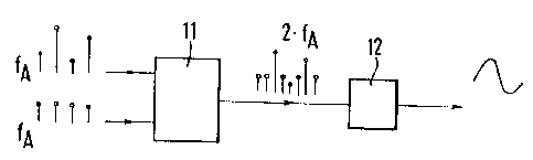
FIG. 1 illustrates a particularly simple structure
for forming an aggregation of time signals according to the
invention, where the respective time signals are input as
sampling values with a sampling frequency fA. In that case the
sampling frequency fA must be larger or at least equal to twice
the bandwidth of the band-limited time signals.
The time signals from both sources are input into a
time-division multiplex unit 11, in which they are offset in
time and superimposed on each other. It is an advantage if the
sampling values of the time signals are equidistant in time, so
that with the present example sampling values with a frequency
of 2-fA emerge from the time-division multiplex unit 11. These
are input into a low-pass filter 12 with a bandwidth B' > B.
The desired composite signal can be tapped off from the output
of the low-pass filter 12.
An improved configuration for the processing of
digital input data is schematically illustrated in FIG. 2. In
that case the digital sampling values, which in the present
example originate once again from two sources only, are input
into the time-division multiplex unit 21, in which a preferably
equidistant time-offset takes place once again. The super-
imposed time-offset signals are then routed to a digital low-
pass filter 22, which is
CA 02230481 1998-04-01
clocked at a frequency of 2 fA in the present example.
Since the digital low-pass filter 22 always produces
periodic continuations of the signals which are not
desirable, the composite signals, after they have passed
through a digital-analog converter ~DAC) 23, are routed
to a further but analog low-pass filter 24 which allows
the small frequency portions of the produced signals to
pass through the frequency space, and dampens the higher
frequencies enough to suppress the undesirable periodic
signal artifacts. In the present example, the DAC 23 as
well as the digital low-pass filter 22 are clocked at a
frequency of 2 ~ fA, since only signals from two different
sources must be processed, which are equidistantly offset
with respect to each other in the time-division multiplex
unit 21. The analog low-pass filter 24 may be an
inexpensive RC element or can be made up of severaJ of
them.
FIGs. 3a and 3b schematically i].lustrate the
sequence of the method of the invention: FIG. 3a
illustrates the time signals of N sources below each
other, where the signals are identified by "S" followed
by a figure for the source number, and another figure for
the sampling value number inside of the next analog
signal. The signals from N different sources are routed
to the multiplex unit 31 which is schematically
illustrated in FIG. 3b, where they are offset in time and
superimposed on each other. The sampling values from the
same source require an equidistant offset in time, while
the signals from different sources need not be
equidistantly offset in time if a filter installation or
a DAC can manage a sufficiently high signal processing
speed.
The resulting signal sequence at the output of the
time-division multiplex unit 31 is routed to a normal
CA 02230481 1998-04-01
low-pass filter 32 whose bandwidth B' corresponds to
about half the sampling frequency f~, so that the signals
of each individual source can be reconstructed from the
composite signal.
FIG. 4 schematically illustrates the processing of
sampling values from signals which are presently analog
and originate from different sources, which are
superimposed and offset in time in a time-division
multiplex unit that is not illustrated further in FIG. 4,
so that all the sampling values from all the other
sources (S21 to SN1) are located between the first
sampling value S11 from the first source and the second
sampling value S12 from the first source. This sequence
is routed to an analog low-pass filter 42 from which a
corresponding continuous composite signal emerges in
analog form.
FIG. 5a illustrates the same process with the
input of digital sampling values. In this case the time-
offset superimposed signals are again routed to a low-
pass filter 52, which is a digital low-pass filter that
is clocked at a frequency of N ~ fA. A composite signal
with digital sampling values of the N fA frequency is
created at the output of the low-pass filter 52 and, as
illustrated in FIG. 5b, are routed to a DAC 53 which is
also clocked at the N fA frequency. The output of the
DAC 53 then contains analog sampling values with an N fA
frequency which, because of the above described mode of
operation of digital low-pass filters, must still undergo
an analog low-pass filtration in an RC element 54.
If the time-flow of the digital sampling values is
divided into equal blocks of n sampling values each, it
is sufficient as a rule to keep the first respective
CA 02230481 1998-04-01
sampling value of each block and to ignore the remaining
sampling values (n - 1). The sampling values selected by
means of this so-called decimation procedure have a
repetition frequency rate fA and also represent the
desired composite signal exactly.
Inversely, an interpolation of sampling values can
take place with the help of a so-called sampling rate
conversion. FIG. 6 schematically illustrates how analog
signals, which emerge offset in time and superimposed on
each other from a time-division multiplex unit 61, are
routed to an analog low-pass filter 62, whose output is
provided with a sample-hold circuit 65. The latter in
turn is connected to an analog-digital converter unit
(ADC) 63, after which a digital processing of the signals
becomes possible. To increase the sampling frequency for
the sampling rate conversion, "zero values" are
interpolatively inserted in areas in which no sampling
values are present.
Finally FIG. 7 schematically illustrates a device
according to the invention, with a time-division
multiplex unit 71, an interpolation device 76 for
inserting "zero values" and the corresponding sampling
rate conversion, a low-pass filter 72 as well as a
decimator 77 for the selective compaction of the signal
data in accordance with the above described decimation
procedure.