Note: Descriptions are shown in the official language in which they were submitted.
CA 02230928 1998-03-02
WO 97/09839 P~CT/FI96/00473
1
Switch with one-bit resolution
The present, invention relates to a method in
accordance with the preamble of the appended claim 1 and a
. 5 switch in accordance with the preamble of the appended
claim 5 for implementing switching c~rith one bit reso-
lution.
In digital transmission systems, data is trans-
mitted in a successive stream of bits or symbols in time
slots in which a predetermined number of bits, typically
eight bits, are transmitted. In convent=Tonal PCM systems,
these bits in one time slot are all reserved for one chan-
nel. In the European 2048 kbit/s basic multiplex system
(in which the frame length is 32 time slots, i.e. 256
bits), altogether 30 speech channels each having a trans
mission rate of 64 kbit/s can be sent in this way. (The
corresponding United States system has 24 channels, the
rate being 1544 kbit/s).
Today, however, sophisticated speech encoding
methods are available for improving the transmission capa
city. The capacity of the above 2048 kbit/s basic system
can be enlarged to 60 or 120 speech channels, for example.
In such a case, the information in the speech channels has
to be coded in a codec.
On account of such encoding methods, one speech
channel thus only occupies some of the bits in the time
slot, e.g. four or two bits out of eight. Codecs are also
available wherewith a band of 7 kHz, for instance, can be
transmitted by employing 6, 7 or 8 bits per time slot,
i.e. by taking up 48, 56 or 64 kbit/s of the capacity of
the basic multiplex system. Such approaches allow sub
channels, such as data channels, to be packed into one
time slot, since less than 8 bits per time slot are needed
' to transmit the actual channel.
As a result of the development described above, a
CA 02230928 1998-03-02
WO 97/09839 PCT/FI96/00473 -
2
need has arisen to switch information to be transferred
with one bit resolution instead of switching byte by byte
(i.e. one word at a time). Such switches operating with
one bit resolution have usually been implemented by using
switching memory circuits having a width of one bit. The '
problem attending such an approach, however, is that the
number of memory circuits increases quadratically in rela-
tion to the number of channels. Consequently, the memory
circuits in practice pose a limitation on the capacity of
the switch, since the physical size and also the power
consumption of the switch rapidly increases to be imprac-
tically high when the number of channels increases.
This drawback also attends the switch disclosed in
PCT application WO 93/16568. This publication discloses a
switch switching on bit level and serving as an aid to a
switch operating on byte level. In this switch, the
switching has two phases in such a way that first the
desired bytes are selected and thereafter the desired bits
are selected from these bytes. The incoming bytes (words)
to the auxiliary switch are first written into speech mem-
ories having a width of one byte, their number being equal
to the number of bits in a byte. Under the control of a
first control memory block, one byte is selected from each
speech memory, and this byte is stored in a corresponding
byte memory. Hence the number of byte memories is equal to
the number of-speech memories. Thereafter, under the.con-
trol of a second control memory block, one bit is selected
from each byte memory for storage in a bit memory. In this
- way, a new PCM word is formed as the output of said
switch.
The drawback attending the above solution is, how-
ever, still the fact that a relatively large number of
memory circuits are needed, since the number of copies of
each incoming byte must equal the number of bits in the
byte. As a result, also the physical size and power con-
CA 02230928 1998-03-02
WO 97/0939 PC'dYFI96/00473
3
sumption of the switch are still relatively high. Further-
more, this solution is intended to serve as a small aux-
iliary switch alongside a switch performing byte-oriented
switching, and is not as such intended as an independent
(high-capacity) switch.
It is an object of the present invention to
provide an improvement in an independent switch with one
bit resolution so as to afford considerably more efficient
memory circuit utilization. This objects is achieved with
the method in accordance with the invention, which is
characterized by what is disclosed in the characterizing
portion of the appended claim 1. The switch in accordance
with the invention is characterized by what is disclosed
in the characterizing portion of the appended claim 5.
The idea of the invention is to implement a switch
in the manner described hereinbelow. 7Cnput links of the
switch are grouped to multiplexers which interleave the
input signals of the switch into a smaller number of
higher-rate serial signals. These signals are stored by
writing the bits of the serial signals into the same mem-
ory location having a width of several bits. This is
preferably carried out in such a way that bits corre-
sponding to each other (i.e. bits occurring in the same
write time slot) are stored at one memory location. In a
preferred embodiment, a memory location corresponds in
width to the number of multiplexers. Reading out from the
memory is carried out in two steps, first selecting the
correct byte from the memory and thereafter selecting the
desired bit from this~byte.
On account of the solution in accordance with the
invention, it is possible to pack data very effectively
' into the memory of the switch. In other words, the switch-
ing memory can be implemented with a minimum of memory
circuits, thus enabling low power~consumption and a small
physical size for the, switch.
CA 02230928 1998-03-02
WO 97/09839 PCT/FI96/00473 -
4
In the following the invention and its preferred
embodiments will be described in greater detail with
reference to examples in accordance with the accompanying -
drawings, in which
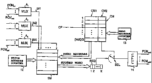
Figure 1 shows a switch in accordance with the
present invention,
Figures 2a and 2b depict two incoming signals to
the switch shown in Figure 1,
Figure 2c illustrates a signal to be stored in the
switch shown in Figure 1,
Figure 3 illustrates storing in a switching memory
shown in Figure 1, and
Figure 4 illustrates a more extensive switch com-
posed of four individual switches.
Figure 1 shows a switch in accordance with the
present invention with one bit resolution. In this exem-
plary case, N incoming serial time-division connections or
links denoted by references PCMini. ~ . PCMinN are connected to
the switch. In each of these incoming signals, the frame
length is K bits, and hence an individual signal has a
maximum of K channels in accordance with the above.
An individual incoming signal may be for instance
the above 2048 kbit/s signal in accordance with the ITU-T
(formerly CCITT) recommendations 6.703 and 6.704 or a
signal having a rate that is a multiple of this basic
rate. If a 2048 kbit/s signal is involved, the frame may __
comprise for example only one channel having a width of
256 bits or 256 channels having a width of one bit, or a
combination of these two extreme cases. In general
outline, a frame of K bits for an individual incoming
signal may comprise 1...K channels each of which has a
width of n bits, n being an integer smaller than or equal
to K. In the following, a rate equal to twice the basic
rate will be employed by way of example, wherein each in-
coming line constitutes a 4096 kbit/s (K=512) serial
CA 02230928 1998-03-02
WO 97/09E39 PCT/FI96/00473
connection, 32 of such incoming signals being provided
(N=32), and hence there is a total of P;xN = 512x32 = 163$4
v
incoming "one-bit channels" to the sw:i.tch, each having
a
capacity of 8 kbit/s. All channels are thus formed from
5 such one-bit channels or multiples thereof. Since, how-
l
ever, the switch of the invention performs switching of
all channels one single-bit "sub-channel" at a time, this
one-bit channel is called a basic channel in this context
(even though it forms only part of a higher-rate channel).
The incoming lines are divided to multiplexers
A1...AX, X multiplexers being provided. Hence, there are
M
- N/X similar signals to each multiplexer. Thus the ratio
of incoming signals and multiplexers is (preferably) such
that the signals can be evenly divided between the mul-
tiplexers. Each multiplexer interleaves the incoming sig-
nals into serial form, and hence the bit rate at the out-
put of each multiplexer is N/X times the bit rate of the
incoming signals. The number X may be e.g. 4, 8 or 16; in
the following a case where X = 4 is exemplified.
Figures 2a and 2b illustrate a first and second
incoming signal for the first multiplexe:r (A1) , i.e. Figure
2a shows an incoming signal from link hCMinl and Figure 2b
shows an incoming signal from link PCMinz. Each bit is
denoted by x. y, where the number x in front of the full
stop indicates the consecutive number of the incoming
signal or link to the multiplexer, and the number y after
the full stop indicates the sequence number of the bit
within the signal frame structure (lsy~K).
A signal IN1 of the kind shown in Figure 2c is
generated at the output of the first multiplexer (A1),
including initially ,the first bit from each incoming
signal, thereafter the second bit from each incoming
signal etc., and lastly the Kith bit from each incoming
signal (N/X of incoming signals being provided). Corre-
spondingly, each multiplexer interleaves the incoming
CA 02230928 1998-03-02
WO 97/09839 PCT/FI96/00473
6
signals into a single serial output signal. Hence, there
is a total of X such output signals, denoted by INl...INX
in Figure 1. ,
The output signals of the multiplexers are stored
in a switching memory SM, having a total of (NxK)/X memory
locations each having a width of X bits. Figure 3 illus-
trates storing in the switching memory. In each time slot
for the incoming signals (i.e. of output signals of the
multiplexers), writing is carried out into the same memory
location having a width of X bits in such a way that in
the first time slot of the frame, the data is written into
memory location 1, in the second time slot of the frame
into memory location 2, etc., and in the last time slot of
the frame into memory location (NXK)/X. (It should be
noted that in this case, the time slot corresponds to one
basic channel.) Hence, the contents of the output signal
frame of the first multiplexer (A1) are stored in bit posi-
tions l, the contents of the output signal frame of the
second multiplexer (AZ) are stored in bit positions 2,
etc., and the contents of the frame for the last
multiplexer (Ax) are stored in the last bit position (X) in
the memory locations of the switching memory.
The write addresses are generated in a write
address counter 12, which increments (in synchronization
with the clock signal on the write side) continually from
one to (NxK)/X (4096 in this exemplary case). The write
operation is carried out cyclically with addresses gener-
ated by counter 12.
There is one outgoing multiplexed 8x4M line (i.e.,
16 standard 2M PCM signals) from the switch of Figure 1.
One memory location is provided in the control memory CM
of the switch for each bit outputted to the line, i.e.
there is a total of NXK/X memory locations. The control
memory is read in step with a read address counter 13. The '
counter increments continually from one to NxK/X. Each
CA 02230928 1998-03-02
w0 97/09839 PCT/FI96/004'73
7
memory location in the control memory CM is bipartite in
such a way that the first part CMl stores the read
a
addresses of the switching memory SM and the bits of the
second part CM2 control a selector SEL. The data stored in
the first part of each memory location indicates the
storage address in the switching memory of the X-bit word
whose bit content (i.e., 8 kbit/s basic rate channel) is
to be switched to the relevant output channel.
Hence, a connection between two channels is estab-
fished when the control memory CM is read cyclically at
addresses generated 'by counter 13, and a read address for
the switching memory SM is obtained from the data in the
control memory. In the switching memory, writing into the
memory constantly alternates with reading out therefrom.
As such, the above arrangement is known from byte-oriented
switches.
By means of, the read address obtained from the
first part of the control memory, the contents of the cor-
responding memory location (in the sw:i.tching memory) are
read into a register REG having a width of X bits. By
means of the control word obtained from the second part of
the control memory on the other hand, the correct bit of
this word which was introduced into the register is
selected with a selector SEL. Hence, one word is read out
into the register per every outputted bit, and the correct
bit is selected from these.
The switching information stored in the control
memory is obtained from a processor unit CP (not shown)
controlling the equipment, which may have received the
information for instance through the signalling network to
which the equipment is connected. Since maintenance of the
contents of the control memory takes place in a manner
known per se and does not relate to tree actual inventive
idea, it will not be described in greater detail in this
context.
CA 02230928 1998-03-02
WO 97/09839 PC'T/FI96/00473
8
Finally, serial connections for the outbound
direction are formed from serial data obtained from the
selector SEL in a manner known per se in a demultiplexer '
unit 14. Since the forming of the outgoing connections is
not within the scope of the actual inventive idea, it will
not be described in greater detail in this context.
The number of outgoing connections M of the basic
block of the above-described switch equals N/X, in other
words, equals the number of connections multiplexed by one
multiplexer. The number of outgoing connections can be
replicated by replicating parts SM, CM, REG and SEL in
Figure 1. In that case, if for example in accordance with
the above preferred embodiment a 64 PCM x 64 PCM switching
matrix (PCM denotes a standard 2M PCM signal) is desired,
four parallel switching memory -control memory -register
-selector combinations are needed, each switching one out-
going 8X4M multiplexed line. During the write phase, the
four-bit 8x4M output signal from multiplexers A1-A4 is
written simultaneously into each of the four switching
memories under the control of a common write address
counter. During the read phase, the word corresponding to
the desired switching stored in the switching memory cor-
responding to each multiplexed 8X4M line is stored in the
register corresponding to the pertinent line. The selector
corresponding to the line selects, under the control of
the control memory, the hit corresponding to the desired
connection from this register. This enables switching of
the desired connection from the four incoming multiplexed
8x4M lines to the four outgoing 8x4M lines. If the read
rate of the switching memory SM can be increased to be
four-fold in relation to the write rate, the switching
memory need not be replicated, but all four control memory
-register -selector combinations may use a switching mem-
ory in common.
In accordance with the invention, incoming PCM
CA 02230928 1998-03-02
WO 97/09839 fCTlFI96/00473
9
connections can easily be added to the combination
described above without adding to the actual switching
equipment. The above-described 64 PCM » 64 PCM switch, for
instance, can easily be expanded into a 256 PCM ~ 64 PCM
switch merely by employing a four-fold number of input
multiplexers and by having a memory width of sixteen bits
in the switching memory (memories).
For example 'a 256 PCM X 256 PCM matrix is corres
pondingly achieved in the manner shown in Figure 4 by
employing four 256 ~PCM x 64 PCM switches SWl...SW4 as
described above in parallel. All swit<~hes are controlled
by a control processor CP through a control bus 42. The
control processor also distributes the necessary clock
signals to all switches. Each switch (SW) interleaves
incoming serial signals PCMini ~ ~ . PCMinaM to a common data bus
42, which in this case has a width of 4X bits, and some
(in this case, a fourth) of the signals are outputted from
each switch. In each,switch, the contents of the data bus
are written into a switching memory, preferably in this
case having a width equal to the number of signals (4X) on
the data bus 42. In each basic switch, the word cor-
responding to the desired channel is read out from the
switching memory, and the selected bit is chosen from this
word by a selector. The above-described more extensive
switch can naturally,also be implemented with one physical
unit.
In each case, the number of serial signals (PCM)
to be switched and the rate of the control/switching mem
ory employed determine how many copies of the switching
memory are to be taken.
Even though ,the invention has been described in
the above with reference to the examples in accordance
with the accompanying drawings, it is obvious that the
invention is not restricted thereto but can be modified
within the scope of the inventive idea disclosed in the
CA 02230928 1998-03-02
WO 97/09839 PCT/FI96/00473
foregoing and in the attached claims.