Note: Descriptions are shown in the official language in which they were submitted.
CA 02231010 1998-03-04
-1-
TITLE OF THE INVENTION
IMAGE DATA STORING METHOD AND IMAGE DATA STORING DEVICE
BACKGROUND OF THE INVENTION
Field of the Invention
The present invention relates to an image data storing
method and image data storing device applicable for various
display devices such as liquid crystal displays, and
particularly to those which can achieve downsizing, and are
lU preferably applied to two-dimensional or three-dimensional
graphics.
Description of Related Art
As is well known, a screen of a liquid crystal display
consists of a lot of pixels arrayed in a matrix. Such a
liquid crystal display generates a picture by controlling
the transmittivity (reflectivity) of all the pixels by
sequentially applying voltages corresponding to pixel data
to liquid crystal elements mounted for individual pixels.
An image data storing device used in such a display
device adopts various design ideas because it is necessary
for a great number of pixel data to be read within a
certain limited time to prevent screen flickering.
Fig. 6 is a block diagram showing a layout of an image
data storing integrated circuit considering such an image
read time. In Fig. 6, reference numerals 51, 52, 53, 54
and 55 each designate a physical bank, a repetition unit of
a memory area in the memory layout; 8s designate memory
buses, each of which has a bus width of m corresponding to
the pixel data, and p (= 4, in Fig. 6) of which are each
CA 02231010 1998-03-04
-2-
connected to the physical banks 51, 52, 53, 54 and 55; and
61, 62, 63 and 64 each designate a memory group, each of
which corresponds to one pixel, and consists of a plurality
of memory elements connected to one of the memory buses 8.
Reference numerals 71, 72, 73 and 74 each designate a group
of n address decoders, each of which is provided for one of
the memory groups for selecting a memory element for
outputting one pixel data. Thus, the total number of
address decoders amounts to pxn. The reference numeral 9
designates a selector for selecting n (= 5 in Fig. 6)
memory buses 8 from among the plurality memory buses 8 to
output the image data on the selected memory buses 8.
Incidentally, the bus width (the number of lines of each
bus) m of each memory bus 8 is determined in accordance
with the number of gray levels of a pixel, and when the
number of bits needed for the pixel is m bits, the bus
width is also set at m in general.
Next, the image data storing method of the conventional
image data storing integrated circuit will be described.
In the foregoing image data storing integrated circuit,
pixels constituting a display picture are divided into
pixel groups, each of which consists of pxn pixels. Then,
the pixel data (1,1), (1,2), ..., and (l, n) in the first
row are stored in the (1,1) memory group 61, (1,2) memory
group 61, ..., and (l, n) memory group 61, respectively.
Likewise, the pixel data (2,1), (2,2), ..., and (2,n) in
the second row are stored in the memory group 62, followed
by storing the third row and onward in the same manner.
Finally, the pixel data (p,l), (p,2), ..., and (p,n) in the
p-th row are stored in the memory group 64.
CA 02231010 1998-03-04
-3-
Next, the read operation of the conventional device
will be described.
In a common image display mode, the pixel data
corresponding to the pixels in the first row are
successively read on every n pixel basis by actuating the n
address decoders 71, ..., 71 while setting the selector 9
such that it outputs the data of the memory groups 61, ...,
61 in the first row, thereby completing the first row.
Likewise, the pixel data corresponding to the pixels in the
second row are successively read on every n pixel basis by
actuating the n address decoders 72, ..., 72 while setting
the selector 9 such that it outputs the data of the memory
groups 62, ..., 62 in the second row, thereby completing
the second row. Thus, all the pixel data of the following
rows are read one after the other.
According to the image data storing integrated circuit,
since the pixel data can be read in groups of n pixels, the
time taken to display a picture is reduced by a factor of
n. This enables the pixel data to be read in a time that
can prevent the flickering of the picture.
In another operation mode of the image data storing
integrated circuit, in which 3-D (three-dimensional)
graphics or the like are carried out, pixel data are
sometimes rewritten column by column at a location in which
a displayed picture changes. In such a case, the p (= 4)
pixel data in each column can be read by actuating the four
address decoders 71, 72, 73 and 74 corresponding to the
physical bank 51 (52, 53, 54 or 55), after setting the
selector 9 such that it outputs the pixel data in the
physical bank 51 (52, 53, 54 or 55).
CA 02231010 1998-03-04
-4-
The conventional image data storing integrated circuit
with the foregoing configuration must possess p sets of
memory buses for each physical bank. As a result, the
number of lines needed for reading the pixel data from each
of the physical banks becomes mxp, amounting to mxnxp lines
for the entire memory. This presents a problem of
hindering downsizing of the memory when handling a large
scale, high gray level display image.
SUMMARY OF THE INVENTION
The present invention is implemented to solve the
foregoing problem. It is therefore an object of the
present invention to provide an image data storing method
and an image data storing device capable of handling a
large scale, high gradation images with reducing the number
of lines of the buses and the size of the memory.
According to a first aspect of the present invention,
there is provided an image data storing device comprising:
a plurality of physical banks, each of which forms a
repetition unit of a memory area, and has a storage
capacity that can store a plurality of pixels in each of a
plurality of pixel groups formed by dividing a display
image; and a plurality of memory buses provided in one to
one correspondence with the plurality of physical banks,
each of the memory buses having a bus width needed for
conveying pixel data associated with at least one of the
pixels, wherein the pixel data stored in the plurality of
physical banks are simultaneously output through the memory
buses to be displayed.
Here, each of the pixel groups may consist of pxn
CA 02231010 2001-11-07
-5-
pixels of the display image, and each of the plurality of
physical banks can store at least p pixels, wherein p and
n are natural number: .
The natural number p may equal n.
The image data storing device may further comprise a
selector for selecting memory buses from among the
plurality of memory ~>uses, wherein the selector may
simultaneously output. one of a set of p pixel data and a
set of n pixel data supplied from the plurality of
physical banks through the memory buses.
The image data storing device may further comprise p
address decoders for selecting memory elements of the
plurality of physical banks in parallel, the memory
elements each storing at least c>ne of the pixel data.
The image data storing device may further comprise an
image data control circuit for controlling such that each
of the plurality of physical banks stores pixels with
their rows and columns different. from each other.
The image data storing device may be formed in an
integrated circuit.
In accordance with one aspect of the present
invention there is provide An image data storing device
comprising: a plurality of physical banks, each of which
forms a repetition unit of a memory area., and has a
storage capacity that can store a plurality of pixels in
each of a plurality of pixel groups formed by dividing a
display image; a plurality of memory buses provided in one
to one correspondence with said plurality of physical
banks, each of said memory buses having a bus width needed
for conveying pixel data associated with at least one of
said pixels; and an image data control circuit for
controlling storing of the pixel data such that each of
CA 02231010 2001-11-07
-5a-
said plurality of physical banks stores pixel data of a
different column anc~ a di.fferent~ row of said pixel groups,
wherein the pixel data stored in said plurality of
physical banks are simultaneously output through said
memory buses to be displayed.
BRIEF DESCRIPTION OF THE DRALVINC~S
CA 02231010 1998-03-04
-6-
Fig. 1 is a block diagram showing a configuration of an
embodiment 1 of an image data storing device in accordance
with the present invention, and its neighboring devices;
Fig. 2 is a block diagram showing a layout of an image
data memory circuit of the embodiment 1;
Fig. 3 is a diagram showing a matrix of pixels in a
liquid crystal display device associated with the
embodiment 1;
Fig. 4 is a block diagram showing a layout of an image
data memory circuit of an embodiment 2 in accordance with
the present invention;
Fig. 5 is a diagram showing a matrix of pixels in a
liquid crystal display device associated with the
embodiment 2; and
Fig. 6 is a block diagram showing a layout of a
conventional image data storing integrated circuit.
DETAILED DESCRIPTION OF THE PREFERRED EMBODIMENTS
The invention will now be described with reference to
the accompanying drawings.
EMBODIMENT 1
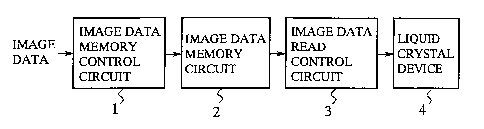
Fig. 1 is a block diagram showing a configuration of an
embodiment 1 of an image data storing device in accordance
with the present invention, and its neighboring circuits.
In Fig. 1, the reference numeral 1 designates an image data
memory control circuit for accepting image data
sequentially input thereto, and for outputting them in
groups consisting of a predetermined number of pixel data;
2 designates an image data memory circuit for storing the
pixel data; 3 designates an image data read control circuit
CA 02231010 1998-03-04
_7_
for reading from the image data memory circuit 2 the image
data in groups consisting of a predetermined number of
pixel data; and 4 designates a liquid crystal device for
carrying out display based on the image. The image data
S memory control circuit 1, image data memory circuit 2 and
image data read control circuit 3 are implemented as an
integrated circuit.
Fig. 2 is a block diagram showing an layout of the
image data memory circuit 2. In Fig. 2, reference numerals
51, 52, 53, 54 and 55 designate n physical banks, each of
which constitutes a repetition unit of a storage area in
the memory layout. Reference numerals 8s designate memory
buses, each of which has a bus width of m corresponding to
the pixel data, and is connected to one of the physical
banks 51, 52, 53, 54 and 55. Reference numerals 61, 62, 63
and 64 each designate a memory group, each of which
corresponds to one pixel, and consists of a plurality of
memory elements. Each physical bank includes four memory
groups 61, 62, 63 and 64. Reference numerals 71, 72, 73
and 74 designate four address decoders for supplying the
memory groups 61, 62, 63 and 64 in the physical banks 51,
52, 53, 54 and 55 with control signals for selecting the
memory elements for outputting the pixel data. The
reference numeral 9 designates a selector for selecting
designated memory buses 8 from among the n memory buses 8
to output the image data on the selected memory buses 8.
Next, the operation of the present embodiment 1 will be
described.
Receiving image data, the image data memory control
circuit 1 supplies the image data memory circuit 2 with
CA 02231010 1998-03-04
_g_
every five pixel data. The image data memory circuit 2
supplies the five image data in parallel to the physical
banks 51, 52, 53, 54 and 55 so that they are stored in the
memory elements designated by the address decoders 71, 72,
73 and 74. Once the pixel data have been stored in the
physical banks 51, 52, 53, 54 and 55 in this way, the image
data read control circuit 3 reads the pixel data therefrom,
and outputs voltage information based on the pixel data.
The liquid crystal device 4 applies the voltages in
response to the voltage information to the liquid crystal
elements to have them display an image formed as a
distribution of their transmittivity (reflectivity).
Next, the storing operation of the present embodiment 1
will be described.
Fig. 3 is a diagram illustrating the pixel matrix in
the liquid crystal device 4, in which a plurality of pixels
are arranged in s rows by r columns. In the present
embodiment 1, it is assumed that the pixel data are input
to the image data memory control circuit 1 in such a manner
that the pixel data of the first row are successively input
from (1,1) in the first column to (l, r) in the r-th column,
followed by the input of the pixel data (2,1) - (2,r) in
the second row, the pixel data (3,1) - (3,r) in the third
row, ..., and finally the pixel data (s,l) - (s,r) in the
s-th row.
In such an input condition, the image data memory
control circuit 1 successively supplies the image data
memory circuit 2 with the pixel data of each row in groups
of every five pixel data.
In the course of this, the image data memory control
CA 02231010 1998-03-04
-9
circuit 1 changes the destination of the output pixel data
for each row. More specifically, as clearly seen by
comparing Fig. 2 with Fig. 3, the destination of the pixel
data are switched such that the first physical bank 51
stores the pixel data (1,1) of the first column of the
first row in the pixel group, the pixel data (2,2) of the
second column of the second row in the pixel group, the
pixel data (3,3) of the third column of the third row in
the pixel group, the pixel data (4,4) of the fourth column
of the fourth row in the pixel group, and again the pixel
data (1,1) of the first column of the fifth row in the
pixel group.
Thus, the pixel data on a display screen is divided
into pixel groups each consisting of 4 rows by 5 columns to
be stored as shown in.Figs. 2 and 3, and each physical bank
stores the pixel data of a different column of a different
row in the pixel group when storing the pixel data.
Next, the read operation of the present embodiment 1
will be described.
First, in an operation mode in which the pixel data are
read row by row, the five pixel data corresponding to the
pixels (1,1) - (1,5) of the first row are read from the
physical banks 51, 52, 53, 54 and 55 by actuating the first
address decoder 71. This operation is repeated until the
pixel data of the first row are completed. Subsequently,
the five pixel data corresponding to the pixels (2,1) -
(2,5) of the second row are read from the physical banks
51, 52, 53, 54 and 55 by actuating the second address
decoder 72, and this operation is repeated until the pixel
data of the second row are completed. Repeating such
CA 02231010 1998-03-04
-10-
operations with the entire rows enables the image data
necessary for generating a picture to be supplied to the
liquid crystal device 4.
Second, in an operation mode in which the pixel data
are read column by column, all the address decoders 71, 72,
73 and 74 are actuated so that four pixel data of the same
column such as (1,1) - (4,1} are read from the physical
banks 51, 52, 53, 54 and 55, followed by the repetition of
the read operation until all the pixel data in the column
are read. The read operation is carried out for the
required number of columns. This enables a part of the
display image to be rewritten to form a new picture.
As described above, the present embodiment 1 comprises
n (= 5) physical banks each including p (= 4) memory
groups, n memory buses each provided for one of the
physical banks, and the selector for selecting a
predetermined number (= 5 or 4) of memory buses from among
the n memory buses to output the image data therefrom.
This makes it possible to reduce the number of buses to the
number of the physical banks. Therefore, the number of the
lines of the memory buses reduces by a factor of p as
compared with that of the conventional image data storing
integrated circuit, and the scale of the selector also
reduces by the factor of p, accordingly. As a result, the
present embodiment 1 can achieve a large scale, high
gradation display with reducing the size of the image data
storing integrated circuit and image data storing device.
Furthermore, since all the physical banks are provided
in common with address decoders for selecting the memory
elements that output the pixel data to the memory buses, it
CA 02231010 1998-03-04
-11-
is not necessary to prepare the address decoders for
respective memory groups as in the conventional image data
storing integrated circuit as shown in Fig. 6. This
enables the number of the address decoder to be reduced by
S a factor n, thereby making it possible to achieve the large
scale, high gradation display with reducing the size of the
memory.
According to the present embodiment l, a display image
is divided into a plurality of pixel groups, each of which
consists of nxp pixels, and each of the physical banks
stores the pixel data of a different column of a different
row in each pixel group. This makes it possible to
simultaneously read not only a plurality of consecutive
pixels in the row, but also a plurality of consecutive
- pixels in the column. Thus, even the device with its size
reduced can rewrite, in groups of every p pixels, only
columns associated with a location in which an image
changes.
EMBODIMENT 2
Fig. 4 is a block diagram showing a layout of the image
data memory circuit in an embodiment 2 of the image data
storing device in accordance with the present invention.
The embodiment 2 differs from the embodiment 1 in that it
comprises four physical banks 51, 52, 53 and 54, and that
the selector 4 is removed. Since the remaining portion is
the same as that of the embodiment 1, the description
thereof is omitted here by designating the corresponding
portions by the same reference numerals.
Next, the operation of the embodiment 2 will be
CA 02231010 1998-03-04
-12-
described.
In this embodiment, the pixel groups, each of which
consists of four rows by four columns, are formed, and the
pixel data stored in the memory groups 61, 62, 63 and 64
vary as shown in Fig. 4. The image data memory control
circuit 1 outputs a group of four pixel data at the same
time, and they are input directly to the physical banks 51,
52, 53 and 54 to be stored. The pixel data output from the
physical banks 51, 52, 53 and 54 are directly supplied to
the image data read control circuit 3. Since the remaining
operation is the same as that of the embodiment 1, the
description thereof is omitted here.
Thus, the embodiment 2 can reduce, besides the effect
and advantages of the embodiment 1, the number of the buses
to that of the physical banks, that is, can reduce the
total number of bus lines by a factor of p as compared with
the conventional image data memory. This is because the
display image is divided into a plurality of pixel groups,
each of which consists of n rows by n columns, where n = 4
in Fig. 4, the physical banks each have a storage capacity
capable of storing at least n pixel data in the pixel
group, and the memory buses, each of which has a bus width
needed for conveying the pixel data, are provided in one to
one correspondence with the physical banks. Furthermore,
the selector can be obviated because the number of lines of
the memory buses equals the number of lines required for
simultaneous reading of the pixel data. As a result, the
large size, high gray-scale can be achieved with reducing
the image data storage.