Note: Descriptions are shown in the official language in which they were submitted.
03,f02J1g98 16:47 9251101 CA 0223l053 l998-03-03 G PAl~iE 0~
" .
~IL ~J~R ~HIS ~ NDED
la
Description
EL~CT~ICI~ METER
The in~ention rela~e~ to ~n elec~rici~y ~eter accordin~ to
the pre~ble o~ ~he pa~ent cl~im 1 (U.S. 4,9g2,7~5)~.
Fro~ ~erman Publish~3d, Nv~-Exa~Lined Patent ~plic~tion DE--OS
37 ~7 053~ ~n inpu~ circ~it of an ~lectricity meter is
~n~wn, in whl~h a differentiating input con~erter is
followe~ ~y Am lnte~r~tor with c1irect-volta~e ne~ativ~
~eedb~ck. The i~egr~tor serves ~o co~pen~te far the
~f~e~entiating ef~ec~ of the input conver~e~. In thi~
ex~mple, tho integrator is embodied as an operatic~n~l
a~plifier wi~h RC ~ ing in the nqgativ~ feecLl~elc:k 3:~ra~ch
The dis~d~a~tage u~ su~h circuits 1~ their in l~g-term
d~ift and the tempe~ature drif~ in the integ~tio~ ~p~itor
di~posed in the neq~tive feed}~X branch~ In acldition,
magnekic ~Lnd electriG int~3r~re~c:e represen~ a problem :t~or
the intes~rator.
In ~ odying the me~er with cli~ital sign~l processing, the
pro~lem also aris~s that th~ componen~ ~secl khere ~r~ v~y
vulne~Lble to interi~erer~ce. Thi~ ~pplies partic~ ly to
volt~ge pe~k~, of the kind that ~c:cur in di~feren~iatin~
conve~ter~, ~or in~t~ e.
~J~; Pa~ent 5,315~36 discloses an electricity meter intend~
:Eor connection to ~ di~feren~ tin~ input con~rerter. The
input conver~er is f~ollowed ~y a di~i~al~'anz~log c:onver~er anc~
a deviGe fo~ disit~l si~nal p~oc~essinSr. Corln~c:teci. bet~een the
input co~ter and th~ ~igitalJanqlcg con~erter is an ~n~log
R3PhACE~NT ~A5ES
03~02~1g98 16: ~7 9251101 CA 0223l0~3 l998-03-0'3~BERG PAGE 03
lb
~ilt~r, which is em~odi~d a~3 ~n ~ctlve lc~w-pass fil~er wi~h
an ~pli~ier. The de~rice ~or di~it~l sig~al proceqslngr
em}~oc3ied a~ a CPU, i~ u5~d to ~;~lcl}late th~ current
c:ons~p~ion i~rom the ~ nput dat:a.
REPI~C~ENT P~GES
E13~'02~19g8 16: 47 g251101 CA 02231053 1 99X 03 03~BEREi PA~;E 04
2a
F~um ~uropean P~t~nt Appl~tion EP O ~34 ~2 Al, the use of
~i~m~-~elta converters and ~ult,pl~x~r~ in ~hree~pha~e
electricity ~eter~ i~ known in principle~
The o~ect of thQ inven~lon i~ t~ dis~lo~e ~n e~ectricity
~e~er with ~if~erentiati~g input ~n~erters ~nd digltal
~ignal proce~in~, in ~hich ~ ~opy of ~he ~easu~e~ ~ignal can
be genexate~ in a reliable w~, wi~h~ut en~Uing signal
~ulter~tion.
The solution o~ the object is ~tt~ined ~cG~rdlng to the
~n~ent~on with an elec~ricity m~t~r ih ~cordance with the
ch~r~eteristics of cl~im 1.
~he filter f~ion of the analoq ~ilter provi~e3 a
limitation for vol~ge pulse~ th~t are o~tput by the input
conve~t~r . ~he variation in th~ input 3ignal is ~e~lne~r
howeYer, ~n~ i~ compensatQd fo~ downstream in khe siqn~l
pro~essi~g. In this w~y, an integr~tin~ ~un~tlon ~or the
di~ferentlating input con~erter and at the ~a~e time
pro~ee~ive ~unekion ~or the inp~ ~e~i~n o~ ~he electronic~
1s provi~ed.
The ~nalog ~llter may ~e emb~died ~ an ~cti~e filter ~ith an
a~plifier. Thi~ ma~es possibl~ an addit$cnal l~vel
~dapta~ion be~ween the input conv~rt~r an~ the downst~e~m
e Lect~b~ic~ r
3~EPI~,~:EMENT P~GES
88~0~1Yg8 16: 4~ 9251101 CA 0223l053 fgg8 03 03 BERG PAGE 05
Prel~er~ly, the analo~ ~ilter is a ~ ~w~pa~~ ~ilter ~ In ~his
way, ~peçial vol~age peaks, whic:h oc~ur particularly a~ the
pha~e
REPI~CE;M~NT PAGES
~ =
- CA 022310~3 1998-03-03
shift and have a higher frequency than the mains frequency,
are limited.
Advantageously, the analog filter is an RC element. This
provides for an especially simple embodiment of the filter
that can also be made economically. Nor do the components
used have to meet such high demands as in the case of the
integration capacitor in a circuit according to the prior
art, for instance.
The analog filter may be a second- or higher-order limiting
filter. In this way, the influence on low frequencies is
very slight. Any drift in the capacitors used has virtually
no effects on angle errors.
Preferably, the analog/digital converter is a sigma-delta
converter ( converter). In this way, precise and rapid
conversion of the input signals is possible, and even the
highest demands, as for precision meters, can be met.
In a special embodiment, a multiplexer is connected between
the analog filters and the analog/digital converter. In
this way, with a single analog/digital converter, a
plurality of input signals can be processed, and each
channel formed is adapted with its filter to the applicable
signals conditions.
Preferably, the electricity meter has at least three input
converters for detecting a three-phase input signal. It can
thus be used in three-phase systems. Advantageously, the
device has a digital signal processor. This makes it simple
to realize the filtering and integrating function.
CA 022310~3 1998-03-03
4a
Preferably, the differentiated signal is embodied as a
current signal. The device may also be additionally
supplied with at least one digitized voltage signal of a
voltage converter, downstream of which is also an analog
filter, and in the device, the voltage signal is carried to
the digital filter or to a further digital filter. In this
way, the compensation algorithm in the digital filter can be
designed very simply.
This embodiment pertains to an application in which current
and voltage are linked together, such as in a power
measurement. Because of the analog filter in the current
detection, a phase displacement occurs, which must be taken
into account in the digital filter. However, if the same
phase displacement occurs for the voltage signal, then the
phase displacement in the digital filter can be dispensed
with. The digital filter need merely compensate the analog
filter in terms of the amount. It is understood that the
voltage detection is preferably effected in three-phase
fashion with three voltage converters, and optionally a zero
current can also be detected. For the voltage detection,
one additional analog/digital converter, optionally preceded
by a multiplexer, may be provided. This provides for
separate signal detection for current and voltage.
The invention, further details, and advantages will be
described below in further detail in terms of exemplary
embodiments and in conjunction with the drawing. Shown are:
Fig. 1, an electricity meter with analog filters;
Fig. 2, a second electricity meter with second-order analog
filters;
CA 02231053 1998-03-03
4b
Fig. 3, a third electricity meter with level adaptation and
impedance conversion; and
Fig. 4, a fourth electricity meter with analog filters in
its voltage detection.
CA 022310~3 1998-03-03
In the drawing figures described below, details that are the
same or function the same are identified with the same
reference numerals, and differences between identical
details in different channels are sometimes identified by
suitable subscripts or additional appended symbols.
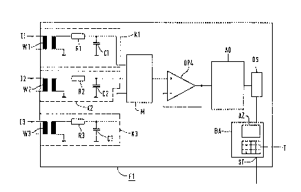
In Fig. 1, an input circuit of an electricity meter E1 is
shown in detail. It has three channels K1, K2, K3, to each
of which a respective one of the current signals I1, I2, I3
of an electrical consumer, not otherwise shown, are supplied
as input signals. Hereinafter, channel K1 will be described
in further detail for each drawing figure, as an example for
all the channels.
The current signal I1 is first supplied to a differentiating
converter W1 in channel K1. Downstream of that is an analog
filter, which is formed by an RC element having a resistor
R1 and a capacitor C1.
This filter is used to limit the voltage peaks that occur at
the output of the converter W1, peaks that can be as high as
several hundred volts and which are very brief in pulse
length. Such voltage peaks occur to an increased extent in
electrical networks in which phase-shift controls are
employed. In that case, in fact, a ma~or change in the
current occurs within a short time. These voltage peaks are
markedly higher than the voltage range on the input side of
the downstream electronics, in particular the downstream
analog/digital converter (hereinafter called converter AD~
and can reach voltage values of up to several hundred volts.
Merely lopping off these voltage peaks would cause an
unacceptably major adulteration in the measurement signal in
the ensuing integration. In a power or energy measurement,
this would lead to a measurement error.
E33f02~11998 1~: 47 9~i!511131 I ERNER GREENBER~i PAGE 136
CA 02231053 1998-03-03
6a
~he c:hann~ls K1, K2, K3 ~re c:onr~ecte~ to one comr~on
multiplexer M, whose output s~ gnal is suppli~d via an
operational amplifi~r OP4 with r~eg~ive f~e~ack tv the
conve~er ~. Th~ put 4 of th~ con~rer~er ~ i ~ c~rriecl
to a deviGe D~ ~or di~ital ~ nal ~rGcessix~g, which performs
d~ta-spe~ific processing of the digltize~ cUrren~ signals
I1-I3 In ~his proces~in~, consumer metering, error
monito~ing, or o~hsr functions ess~ntial ~or prote~tion or
counting purposes ~an be pe~foLmed. It i-q ~n~erstood that
for cal~:ul~Ltiny power, ~he device ~S can also be sup~?lied
~ith ~dditionai voltage ~igr.~ls of the ~e~pec~tive co~lmer
via Gh~nnels not shown in further detail. By way Of
exampl~, the digital de~i~e ~S may b~ embodi~d as a c~i~it~l
~ignF~l pro~es~or or as ~ comput~tion cl~vi~e w~h a
micropr4~es~0r .
The cl~7ice 1~ is ~ollowecl dowrlstream by an irl,pu~ a~.d displ~y
device ~A, which includ~s ope~tor control means, s~h ~ a
ke!yboarcl T ~nd display me~ns AZ. The operator cont~ol and
di~play ar~ngement 3A c~n also h~e an int~rface STt which
i5 use~ ~or dat~ excha~ge, fo~ instance wi~h a ~and-~eld
ter~in~l or higher-leve~ cont~ol de~ice~ for re~ote pollin~.
integratlon ~un~tio~ is realized in the ~evic~ DS with an
di~it~l fiLter. Thi~ integr~tion f~nction is use~ ~o
compens2te for the differenti~t~ng infl~enc:e o~ the input
con~er~ers Wl, W~, W3.
The analog f~l~er~ ll~it th~ vario~s p~lses OF sign~l~ an~
the ~ame time propag~te the~. Hence the si~al ~comes
adulterate~ in ~gnitude/a~unt an~ ~ngle, a~ a ~nCtion of
t~e fr~aue~cy. This adulteratio~ is compensa~ed for in th~
d~ e DS with the ai~ of ~n ~d~itio~1 digital filter. ~hi~
addit~onal digit~l filte~ has an i~ver~ transfer functlon to
RE~LA~EME~T ~A~
33~02~1g93. 1~ 7 92511~1 L~N~I~ r;~ NBEP.G PkGE 07
6b
~hat o~ th~ analog fllte~ n thi~ way, the in~luenc~ of thP
filter~ on ~he transfer
~EPLACEM~Ntr PAGES
CA 022310~3 1998-03-03
7a
function to that of the analog filter. In this way, the
influence of the filters on the transfer function in the
lower frequency range is substantially eliminated.
The transfer function of the analog filters is as follows:
1 + ja~RC
A simulation of an RC member as a digital filter, with the
aid of a bilinear transformatio n, furnishes the following
transfer function for the Z range:
A(z)=
1 -~z-
To compensate for the analog filter using the digital
filter, the inverse transfer function as follows is
necessary:
1 _ ~lZ-l
Since A(z) and A(~) agree only for very high scanning rates,
a further adaptation must be performed with the aid of delay
members. This means that the filter to be made must
preferably be of a higher order. One example of a possible
transfer function is shown below.
B(z) = - 1 -2 -3 -4
o~ + ~lZ + ~2Z + ~3Z + ~4Z
In this last equation, the symbols have the following
meanings:
~ CA 02231053 1998-03-03
7b
R resistance
C capacitance
~ circuit frequency
a, ~, z coefficients
CA 022310~3 1998-03-03
8a
The values for the various coefficients can be specified by
one skilled in the art, using the methods familiar to him.
Fig. 2 shows another variant of an electricity meter E2,
which in principle has the same layout as the electricity
meter E1 of Fig. 1. Here for the sake of simplicity the
operational amplifier OP4 is omitted.
In this version, K1, K2, K3 have a higher-order, in
particular a second-order, band limitation filter as their
filter. To that end, the low-pass filter with the resistor
R1 and the capacitor C1 is followed by an operational
amplifier OP1 with a voltage divider comprising the
resistors R11 and R12 and a positive feedback capacitor C11.
In this way, the influence on low frequencies is very
slight. The drift in the capacitors, especially the
capacitor C1, thus has only a slight effect on the resultant
angle errors.
Fig. 3 shows a further version, which compared with the
version of Fig. 2 has a simplified layout. Here the
components R1 and C1, specifically, are omitted. With this
version, which includes a first-order filter, compared with
the version of Fig. 1, level adaptation and impedance
conversion are possible. This is attained by providing that
the filter includes an active component, namely the
operational amplifier OP1 as its amplifier.
Fig. 4 shows an electricity meter E4 in accordance with the
version E1 of Fig. 1, but in which in addition voltage
signals are processed, for instance for energy measurement.
For the sake of simplicity, only one voltage channel Ku and
one current channel Ki are shown, which are carried to a
common multiplexer M. It is understood that once again a
separate channel formation with separate multiplexers and
CA 02231053 1998-03-03
8b
analog/digital converters is actually preferred. Both
channels Kn and Ki have a first-order analog filter.
03~02.'~gc8 1~: ~7 9~511~1 CA 02231053 1998-o3-o33ERG PAGE e8
.
I'he analog filters are em~odied i~ such a r,Jay ~h~t for the
various ~ als they cause ~he same pha~e di~plzc:emen'c. As
a result, this sisnal adulteration rleecl rlot be takeT~ into
acc~ur~t~ in t~e device DS, whic~ ~hu~ economizes on
computatioIl time. Th~ cligital ~ilter ~or compensating ~or
the ~nalog 4'~ ~ter or ~il~ers neecl mere~y corhpe~sate in te~ns
of the ~mount . 'rhls sir~plii~ie~ the compens~ti~n ~1 gori~hm
Pr~ferably ~ mc~dulator is used for ~he conver~er AD. I~
i~ dist~n~uis~ed b~ ~avor~ proper~le~ ~or u~se :~n
consur~ption ~e~urelr;en~; by the spec~ fica~ion o~ ~-er~in
para~eters, o~timal ad~ptation with regard to proces~ ng
time ancl aGc~cy can be ~chie~ed t~ thQ ~r~ricuS kinds o~
s~ gnal proces~ing. Hawe~er, other embodimen~s are alsc~
poss ibie
RE~?I~CE~NT PAG~5