Language selection

Search

Patent 2231306 Summary

Third-party information liability

Some of the information on this Web page has been provided by external sources. The Government of Canada is not responsible for the accuracy, reliability or currency of the information supplied by external sources. Users wishing to rely upon this information should consult directly with the source of the information. Content provided by external sources is not subject to official languages, privacy and accessibility requirements.

Claims and Abstract availability

Any discrepancies in the text and image of the Claims and Abstract are due to differing posting times. Text of the Claims and Abstract are posted:

  • At the time the application is open to public inspection;
  • At the time of issue of the patent (grant).
(12) Patent Application: (11) CA 2231306
(54) English Title: IMPROVED MONOLITHIC INTEGRATED CIRCUIT AND ANTENNA COIL STRUCTURE COMPRISING A PERIPHERAL PROTECTIVE RING
(54) French Title: STRUCTURE AMELIOREE A CIRCUIT INTEGRE MONOLITHIQUE ET A BOBINE D'ANTENNE COMPORTANT UN ANNEAU PROTECTEUR PERIPHERIQUE
Status: Deemed Abandoned and Beyond the Period of Reinstatement - Pending Response to Notice of Disregarded Communication
Bibliographic Data
(51) International Patent Classification (IPC):
  • H01Q 23/00 (2006.01)
  • G06K 19/077 (2006.01)
  • H01Q 1/22 (2006.01)
  • H01Q 1/38 (2006.01)
  • H01Q 1/48 (2006.01)
  • H01Q 7/00 (2006.01)
  • H01Q 7/04 (2006.01)
  • H04B 1/59 (2006.01)
(72) Inventors :
  • KUNZ, PASCAL (Switzerland)
(73) Owners :
  • EM MICROELECTRONIC-MARIN SA
(71) Applicants :
  • EM MICROELECTRONIC-MARIN SA (Switzerland)
(74) Agent: GOWLING WLG (CANADA) LLPGOWLING WLG (CANADA) LLP
(74) Associate agent:
(45) Issued:
(22) Filed Date: 1998-03-05
(41) Open to Public Inspection: 1998-09-24
Examination requested: 2002-03-21
Availability of licence: N/A
Dedicated to the Public: N/A
(25) Language of filing: English

Patent Cooperation Treaty (PCT): No

(30) Application Priority Data:
Application No. Country/Territory Date
0702/97 (Switzerland) 1997-03-24

Abstracts

English Abstract


The present invention concerns an integrated circuit
structure (1) formed in a substrate (2) and including at
least one integrated circuit element (3, 4), an antenna
coil (5) capable of transmitting and/or receiving data,
and associated with said integrated circuit element(s) (3,
4); and a metal protective ring (20) situated at the
periphery of the integrated circuit structure (1). The
present invention is characterised in that said protective
ring (20) comprises at least one ohmic interruption, so
that it does not form a closed circuit on itself. The
integrated circuit structure (1) according to the
invention is improved in that the operation of the antenna
coil (5) is made insensitive to the presence of the
protective ring (20).


French Abstract

La présente invention porte sur une structure à circuit intégré (1) formée sur un substrat (2) qui comporte au moins un élément à circuit intégré (3, 4), une bobine d'antenne (5) capable d'émettre et/ou de recevoir des données associée à ces éléments à circuit intégré (3, 4), et un anneau protecteur métallique (20) monté à la périphérie de cette structure à circuit intégré (1). L'invention est caractérisée par le fait que l'anneau protecteur (20) comporte au moins une discontinuité électrique et ne constitue pas un circuit fermé. La structure à circuit intégré (1) de l'invention est améliorée du fait que le fonctionnement de la bobine d'antenne (5) est insensible à la présence de l'anneau protecteur (20).

Claims

Note: Claims are shown in the official language in which they were submitted.

- 4 -
WHAT IS CLAIMED IS
1. An integrated circuit structure formed in a
semiconductor substrate and including:
- at least one integrated circuit element;
- an antenna coil arranged to transmit and/or
receive data, and be connected with said at least one
integrated circuit element; and
- a metal protective ring situated at the periphery
of said integrated circuit structure;
wherein said protective ring is arranged with at least one
ohmic interruption, so that it does not form a closed
circuit on itself, which makes the operation of the
antenna coil insensitive to the presence of the protective
ring.

Description

Note: Descriptions are shown in the official language in which they were submitted.


CA 02231306 1998-03-0~
Case 1515
AG/kdp
IMPROVED MONOLITHIC INTEGRATED CIRCUIT AND ANTENNA COIL
STRUCTURE COMPRISING A PERIPHERAL PROTECTIVE RING
The present invention concerns a monolithic
integrated circuit structure and, more particularly, a
monolithic structure essentially including an antenna coil
provided with a peripheral protective ring.
Structures including integrated circuits and an
antenna coil are conventionally used, in particular for
making a transceiver which is generally called a
" transponder N, By way of example, WO 88/00785 discloses
a transponder device including a monolithic structure 1
formed in a substrate 2, and comprising different
integrated circuits 3, 4 and an antenna coil 5, as is
shown in Figure 1 by way of illustrative example. In this
example, coil 5 is formed by several conductive turns 6
which surround different logic circuits 3, 4.
Moreover, during manufacturing of the mask intended
to make the structures of the aforementioned type, a metal
protective ring 8 is generally formed at the periphery of
structure 1, as is shown in Figure 1. A protective ring of
this type usually has numerous advantages in that it
protects structure 1 against mechanical stress exerted on
the different layers deposited on substrate 2 during
dicing of the integrated circuits formed on substrate 2,
in that it allows a high quality finish of the edges of
the integrated circuits, and in that it avoids corrosion
of integrated circuit elements 3, 4 and 5.
However, the Applicant has observed that, in such
structures, the metal protective ring forms what may be
called a parasitic short-circuit turn for the elements
situated within said turn, in particular the antenna coil.
Essentially, this parasitic turn surrounding the antenna
coil affects in particular the action of external fields
intended essentially for said coil, which causes
undesirable disturbances in the operation thereof.

. CA 0223l306 l998-03-0
- 2 -
It goes without saying that an integrated circuit
structure in which the coil does not necessarily surround
all the integrated circuit elements, has the same
malfunction.
An object of the present invention is to provide an
improved integrated circuit structure including in
~ particular an antenna coil and a peripheral protective
ring, in order to avoid disturbed operation of said coil.
This object, in addition to others, are achieved by
the improved integrated circuit structure formed in a
substrate and including:
- at least one integrated circuit element;
- an antenna coil capable of transmitting and/or
receiving data, and associated with said at least one
integrated circuit element; and
- a metal protective ring situated at the periphery
of said integrated circuit structureisaid structure being
characterised in that said protective ring includes at
least one ohmic interruption, so that it does not form a
closed circuit on itself, which makes the operation of the
antenna coil insensitive to the presence of the protective
ring.
An advantage of the present invention is to provide
such a structure fitted with a non-continuous peripheral
protective ring all the way along the periphery of said
structure, which avoids said ring forming a peripheral
closed circuit.
The objects, features and advantages of the present
invention, will appear more clearly upon reading the
detailed description of a preferred embodiment of the
invention, given solely by way of example, in relation to
the annexed drawings, in which :
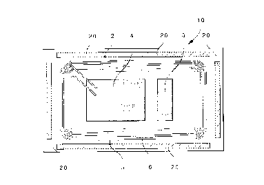
- Figure 1, already cited, shows an integrated
circuit and antenna coil structure according to the prior
art; and
- Figure 2 shows an integrated circuit structure
surrounded by an antenna coil and a protective ring
according to the invention.

- CA 02231306 1998-03-0
_ 3 _
An integrated circuit structure 10 shown in Figure 2
is close to the integrated circuit structure described
hereinbefore. For the sake of simplicity, the components
shown in Figure 2 and designated by the same references as
those shown in Figure 1 are substantially identical to
those designated in Figure 1.
Integrated circuit structure 10 formed in a
monolithic manner in a substrate 2 consists of various
integrated circuit elements 3, 4 and an antenna coil 5
formed by several conductive turns 6 which surround, in
this example, the various logic circuit elements 3, 4.
Integrated circuit structure 10 further includes a
protective ring 20 formed at the periphery of integrated
circuit structure 10, by manufacturing methods commonly
known to the man skilled in the art. Protective ring 20 is
designed so that it does not form a circuit closed on
itself. Protective ring 20 is therefore provided with
ohmic interruptions. It goes without saying that the four
ohmic interruptions of protective ring 20 are only shown
by way of illustration in Figure 2.
By way of alternative, other embodiments of
protective ring 20 may be provided. For example, the shape
of the protective ring may be modified according to the
shape of the integrated circuit structure at the periphery
of which the protective ring is formed.
The fact of locally cutting metal protective ring 20
by at least one ohmic interruption of protective ring 20
thus avoids formation of a parasitic short-circuit turn as
described hereinbefore, which makes the operation of
antenna 5 insensitive to the presence of protective ring
20.
It goes without saying for the man skilled in the art
that the detailed description hereinbefore may undergo
various modifications without departing from the scope of
the present invention.

Representative Drawing
A single figure which represents the drawing illustrating the invention.
Administrative Status

2024-08-01:As part of the Next Generation Patents (NGP) transition, the Canadian Patents Database (CPD) now contains a more detailed Event History, which replicates the Event Log of our new back-office solution.

Please note that "Inactive:" events refers to events no longer in use in our new back-office solution.

For a clearer understanding of the status of the application/patent presented on this page, the site Disclaimer , as well as the definitions for Patent , Event History , Maintenance Fee  and Payment History  should be consulted.

Event History

Description Date
Inactive: IPC from MCD 2006-03-12
Application Not Reinstated by Deadline 2004-03-05
Time Limit for Reversal Expired 2004-03-05
Deemed Abandoned - Failure to Respond to Maintenance Fee Notice 2003-03-05
Letter Sent 2002-07-11
Letter Sent 2002-04-30
Request for Examination Requirements Determined Compliant 2002-03-21
All Requirements for Examination Determined Compliant 2002-03-21
Request for Examination Received 2002-03-21
Application Published (Open to Public Inspection) 1998-09-24
Inactive: First IPC assigned 1998-06-18
Classification Modified 1998-06-18
Inactive: IPC assigned 1998-06-18
Inactive: Filing certificate - No RFE (English) 1998-05-22
Filing Requirements Determined Compliant 1998-05-22
Application Received - Regular National 1998-05-21

Abandonment History

Abandonment Date Reason Reinstatement Date
2003-03-05

Maintenance Fee

The last payment was received on 2002-03-05

Note : If the full payment has not been received on or before the date indicated, a further fee may be required which may be one of the following

  • the reinstatement fee;
  • the late payment fee; or
  • additional fee to reverse deemed expiry.

Please refer to the CIPO Patent Fees web page to see all current fee amounts.

Fee History

Fee Type Anniversary Year Due Date Paid Date
Application fee - standard 1998-03-05
Registration of a document 1998-03-05
MF (application, 2nd anniv.) - standard 02 2000-03-06 2000-02-22
MF (application, 3rd anniv.) - standard 03 2001-03-05 2001-02-22
MF (application, 4th anniv.) - standard 04 2002-03-05 2002-03-05
Request for examination - standard 2002-03-21
Owners on Record

Note: Records showing the ownership history in alphabetical order.

Current Owners on Record
EM MICROELECTRONIC-MARIN SA
Past Owners on Record
PASCAL KUNZ
Past Owners that do not appear in the "Owners on Record" listing will appear in other documentation within the application.
Documents

To view selected files, please enter reCAPTCHA code :


To view images, click a link in the Document Description column. To download the documents, select one or more checkboxes in the first column and then click the "Download Selected in PDF format (Zip Archive)" or the "Download Selected as Single PDF" button.

List of published and non-published patent-specific documents on the CPD .

If you have any difficulty accessing content, you can call the Client Service Centre at 1-866-997-1936 or send them an e-mail at CIPO Client Service Centre.


Document
Description 
Date
(yyyy-mm-dd) 
Number of pages   Size of Image (KB) 
Representative drawing 1998-09-28 1 19
Abstract 1998-03-05 1 20
Description 1998-03-05 3 142
Claims 1998-03-05 1 16
Drawings 1998-03-05 1 75
Cover Page 1998-09-28 1 61
Courtesy - Certificate of registration (related document(s)) 1998-05-25 1 116
Filing Certificate (English) 1998-05-22 1 163
Reminder of maintenance fee due 1999-11-08 1 111
Acknowledgement of Request for Examination 2002-04-30 1 179
Courtesy - Abandonment Letter (Maintenance Fee) 2003-04-02 1 178
Correspondence 2002-07-11 5 21
Correspondence 2002-07-11 2 65