Note: Descriptions are shown in the official language in which they were submitted.
CA 0223162~ 1998-03-09
- 1 - CFO 12645 ~S
SEMICONDUCTOR SUBSTRATE HAVING COMPOUND SEMICONDUCTOR
LAYER, PROCESS FOR ITS PRODUCTION, AND ELECTRONIC
DEVICE FABRICATED ON SEMICONDUCTOR SUBSTRATE
BACKGROUND OF THE INVENTION
Field of the invention
This invention relates to a semiconductor
substrate and a process for its production. More
particularly, it relates to a semiconductor substrate
comprising a silicon substrate and a single-crystal
compound semiconductor formed thereon, suited for the
fabrication of electronic devices and formation of
integrated circuits, and to a process for its
production. It also relates to an electronic device
fabricated on this semiconductor substrate.
Related Background Art
Group IV elements belonging to Group IV of the
periodic table, such as Si and Ge, have been used from
old times as materials for substrates (wafers) for
semiconductor devices and have highly advanced. At
present too, as well known, a variety of electronic
devices such as DRAMs, MPUs, logic ICs and analog ICs
are fabricated on silicon (Si) substrates, and these
elements are utilized as materials for active regions
of diodes, MOS transistors and bipolar transistors.
These Group IV elements, however, are not suited for
making up light-emitting diodes.
CA 0223162~ 1998-03-09
Meanwhile, Group III-V or II-VI compound
semiconductors as typified by GaAs, GaP, InP, GaN and
ZnSe are very suited for light-emitting devices such as
LEDs and lasers. Researches are made thereon in great
variety, and LEDs and semiconductor lasers have already
been put into practical use. Also, HEMTs (High
Electron Mobility Transistors) are prepared using these
compound semiconductors, and high-frequency circuits
that can be used at GHz band regions have been put into
practical use.
Compound semiconductor substrates, however, have
so low a mechanical strength that it is difficult to
produce large-area wafers of compound semiconductors.
Accordingly, such wafers have a fairly smaller size
than silicon wafers, and hence are obtained at a lower
production efficiency than silicon wafer processes.
Moreover, the production cost of the wafer themselves
is a little more than 10 times that of silicon wafers
having the same size.
To overcome such problems, it is attempted to make
heteroepitaxial growth of compound semiconductors on
the silicon substrates that have a high mechanical
strength and enable production of large-area wafers, as
typified by GaAs on Si. This technique is a method by
which light-emitting devices or high-speed electronic
devices such as LEDs and lasers making use of compound
semiconductors are formed on silicon substrates having
CA 0223162~ 1998-03-09
a high mechanical strength and also being inexpensive
and still also having a high thermal conductivity,
thereby aiming at imp~ov~ -nt of productivity,
achievement of cost reduction and so forth and spread
of these devices. In addition, since such
light-emitting devices and high-speed electronic
devices can be integrated on the same substrates as
those of highly advanced Si-LSIs, it becomes possible
to realize Opto-Eletronic Integrated Circuits (OEICs).
However, some problems are pointed out in respect
of the growth of compound semiconductors on such Si,
and there are many difficulties in the fabrication of
devices by the use of the compound semiconductors grown
on Si.
One of them is the occurrence of antiphase domains
caused by polarity/non-polarity, which causes a great
stress or lattice imperfections in epitaxial layers.
The other is the presence of a difference in
coefficient of thermal expansion and a lattice
mismatch, which causes a stress or lattice
imperfections between silicon substrates and compound
semiconductor films.
The former can be restrained by using silicon
substrates having off-angles. The latter can not be
settled with ease, and many research institutes have
made studies on various crystal growth techniques, but,
at present, can not still break the barrier of 106/cm2
CA 0223162~ 1998-03-09
with ease in respect of the dislocation density that
can be an indication of crystal quality. This is said
to be due a lattice strain caused by disagreement in
lattice constant between silicon substrates and
compound semiconductor layers. Lattice defects brought
in at a high density may deteriorate device
characteristics such as light-emitting characteristics
and lifetime, and are not practical. Accordingly, it
is sought to form on silicon substrates, III-V or II-VI
compound semiconductor thin films having a low defect
density comparable to compound wafers.
Many studies on single-crystal semiconductor films
of IV-IV compounds such as SiC and SiGe are also
reported as light-emitting materials, and these
slngle-crystal compound-semiconductor films are also
desired to be formed on silicon substrates. Thus, for
similar reasons, it has been strongly demanded to
decrease such crystal defects also when the
single-crystal films of SiGe or SiC IV-IV compound type
ones are formed on silicon substrates.
As discussed above in detail, the demand for
heteroepitaxy by which single crystals having a good
crystal quality are grown on silicon substrates is at a
high level, but there is still only a low possibility
of accomplishing it.
Many reports are made on heteroepitaxial growth on
such silicon substrates.
CA 0223162~ 1998-03-09
Some reports have presented an attempt to form a
porous silicon layer on the surface of a silicon
substrate and make heteroepitaxial growth on that layer
so as to decrease the crystal defects.
Ohmachi et al. have reported in The Society of
Applied Physics 1987 20aX5, "GaAs Growth on Porous Si",
NTT ECL Y. Ohmachi, W. Watanabe, Y. Kadota and H.
Okamoto, that there are differences in surface
properties and half width between an offset substrate
and a just substrate when crystals are grown by MOCVD
(Metal Organic Chemical-Vapor Deposition) and MBE
(Molecular-Beam Epitaxy) on 10 ,um thick porous silicon
substrates.
It is also known that, when GaAs crystals are
grown by MBE on 10 ~m thick porous silicon substrates,
their cross-sectional TEM observation reveals the
presence of more defects than GaAs crystals grown on
silicon substrates under the same conditions.
Thus, some attempts to improve crystal quality by
the use of porous silicon are reported. Although the
crystal strain of compound semiconductor layers formed
by heteroepitaxial growth can be relieved in some
instances, the compound semiconductors have so poor a
crystal quality that it has been very difficult to
apply them to devices.
In heteroepitaxial growth on silicon substrates
having a main plane of (100)-plane in plane direction,
CA 0223162~ 1998-03-09
the films grown commonly have rough surfaces. To solve
this problem, it has been necessary to use what is
called an offset substrate, in which the plane
direction is angled by some degrees from the
(110)-plane. The PA of Fig. 3 shows an off-angle
dependence of surface roughness (average square
roughness). In order to attain good surface
morphology, the off-angle must be precisely controlled.
Such precise control has tended to bring about an
increase in yield and in substrate cost as well.
Meanwhile, in homoepitaxy on porous silicon
substrates, the present inventors have discovered that,
in silicon homoepitaxial growth by heat CVD using a
source gas diluted with hydrogen, the crystal quality
can be improved when surface pores are stopped up by
hydrogen prebaking carried out immediately before the
source gas is supplied (N. Sato, K. Sakaguchi, K.
Yamagata, Y. Fujiyama and T. Yonehara, J. Electrochem.
Soc. 142 (1995), p.3116).
Figs. 2A and 2B are diagrammatic illustrations to
describe a process in conventional techniques. In
Figs. 2A and 2B, reference numeral 20 denotes a porous
layer (porous silicon substrate); 21, walls of the
porous layer; 22, pores of the porous layer; 24, a
single-crystal compound-semiconductor film; and 25,
crystal defects.
First, a porous silicon substrate 20 is prepared
CA 0223162~ 1998-03-09
(Fig. 2A). Next, the porous silicon substrate 20 is
placed in a reaction chamber of a CVD apparatus, and a
single-crystal film 24 of a compound semiconductor such
as GaAs is formed by heteroepitaxial growth on the
porous silicon substrate, using trimethyl gallium
(TMGa) or arsine (AsH3) as a source gas (Fig. 2B).
In the single-crystal compound semiconductor film
24 thus formed, crystal defects 25 due to strain,
lattice mismatch and grain boundaries are produced on
the side of the surface 26 of the porous silicon
substrate 20.
SUMMARY OF THE INVENTION
An object of the present invention is to provide a
semiconductor substrate as a large-area silicon
substrate on which a single-crystal
compound-semiconductor film having less crystal defects
can be formed in a high productivity, a high
uniformity, under a high controllability and at a low
cost.
Another object of the present invention is to
provide a process by which a single-crystal
compound-semiconductor film having smooth surface and
less crystal defects can be formed on a large-area
silicon substrate where the offset (off-angle of plane
direction) is not particularly specified.
To achieve the above objects, the present
CA 0223162~ 1998-03-09
invention provides a semiconductor substrate comprising
a silicon substrate having a porous region, and a
semiconductor layer provided on the porous region,
wherein;
the semiconductor layer comprises a single-crystal
compound semiconductor and is formed on the surface of
the porous region with its pores having been sealed at
the surface.
The present invention also provides a process for
producing a semiconductor substrate, comprising the
steps of;
heat-treating a silicon substrate having a porous
region, to seal pores at the surface of the porous
region; and
forming a single-crystal compound-semiconductor
layer by heteroepitaxial growth on the porous region
having the pores sealed by the heat treatment.
According to the present invention, a compound
semiconductor layer having a good crystal quality and a
smooth surface can be formed over a large area on a
silicon substrate the off-angle of plane direction of
which is not particularly specified.
In particular, the compound semiconductor layer
having both a good crystal quality and a smooth surface
can be formed by heteroepitaxial growth over a large
area at one time even on substrates having a low
off-angle, e.g., silicon substrates having an off-angle
CA 0223162~ 1998-03-09
within 1~ with respect to the (100)-plane, which are
commercially available in variety.
According to the present invention, a
semiconductor device, a semiconductor substrate and a
process for its production can be provided which can
answer the problems the prior art has had. More
specifically, compound semiconductor substrates with a
high quality can be produced using inexpensive silicon
substrates, and, using such substrates, compound
semiconductor devices with good characteristics can be
fabricated at a low cost.
BRIEF DESCRIPTION OF THE DRAWINGS
Figs. lA, lB and lC are diagrammatic
cross-sectional views to describe a process of the
present invention.
Figs. 2A and 2B are diagrammatic cross-sectional
views to describe a process of the prior art.
Fig. 3 is a graph showing the relationship between
off-angles and surface roughness of substrates.
Fig. 4 is a cross-sectional view of a solar cell
as a photoelectric transducer (photovoltaic device)
according to the present invention.
Fig. 5 is a cross-sectional view of an LED as a
light-emitting device according to the present
invention.
Fig. 6 is a cross-sectional view of a
CA 0223162~ 1998-03-09
-- 10 --
semiconductor laser as a light-emitting device
according to the present invention.
Fig. 7 is a cross-sectional view of an HEMT as a
transistor according to the present invention.
DESCRIPTION OF THE PREFERRED EMBODIMENTS
In an embodiment of the present invention, before
a single-crystal compound semiconductor layer is formed
by heteroepitaxial growth on a porous silicon
substrate, the substrate is heat-treated in an
atmosphere of hydrogen, whereby a single-crystal
compound semiconductor layer improved in crystal
quality can be formed on the silicon substrate, the
compound semiconductor layer with a good crystal
quality can be formed on the silicon substrate
surpassingly in view of productivity, uniformity,
controllability and economical advantages, and also a
semiconductor substrate production process can be
proposed which can be applied to conventional compound
semiconductor devices while ensuring their advantages.
In another embodiment of the present invention,
pores at the surface of porous silicon formed by
processing a silicon substrate originally having a good
crystal quality are sealed by heat treatment while
supplying a trace amount of silicon, to form thereon a
single-crystal compound-semiconductor layer with a good
quality. Thus, a large number of substrates can be
CA 0223162~ 1998-03-09
processed at one time, and their crystal quality can be
improved to a level comparable to or higher than that
of single-crystal compound-semiconductor substrates
themselves without lowering their productivity and
economical advantages.
In the present invention, pores at the surface of
porous silicon formed by processing a silicon substrate
originally having a good crystal quality are sealed by
heat treatment while supplying a trace amount of
silicon, to form the single-crystal
compound-semiconductor layer over a large area at one
time without bringing in the single-crystal
compound-semiconductor layer any crystal defects due to
strain and lattice mismatch. Thus, photoelectric
transducers such as solar cells, light-emitting devices
such as lasers and light-emitting diodes and
transistors such as HEMTs can be formed on such
single-crystal compound-semiconductor layers while
ensuring the characteristics comparable to instances
where they are formed on single-crystal
compound-semiconductor substrates themselves, and also
can be formed surpassingly in view of productivity,
uniformity, controllability and economical advantages.
The present invention will be described below in
detail with reference to the accompanying drawings.
Figs. lA to lC are diagrammatic cross-sectional
views showing a process for producing a semiconductor
CA 0223162~ 1998-03-09
- 12 -
substrate as a preferred embodiment of the present
invention.
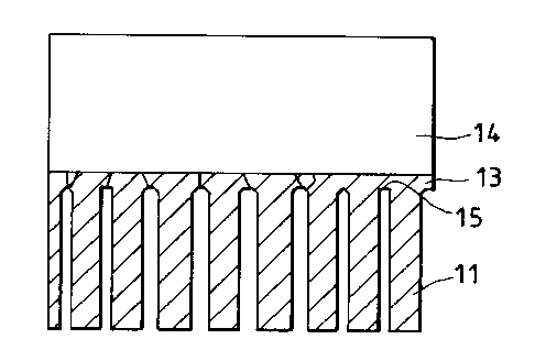
In Figs. lA to lC, reference numeral 10 denotes a
silicon substrate having a porous region, which has
pores 12 of the porous region and walls 11 that form
the pores. In the drawing, the pores 12 are
illustrated in a simple form for the purpose of easy
understanding. Actually, in many cases, the pores 12
have a complicated form like branched open pores.
As shown in Fig. lA, first, the silicon substrate
10 having a porous region is prepared (Fig. 2A). Such
a silicon substrate 10 may be obtained by anodizing a
commonly available silicon wafer (non-porous silicon
substrate), whereby the whole wafer or only the surface
portion of the wafer can be made porous.
Next, the silicon substrate 10 having a porous
region is heat-treated in an atmosphere of hydrogen.
As a result of this heat treatment in an atmosphere of
hydrogen, native oxide films unwantedly formed on the
surface of the substrate are removed. The native oxide
films are removed by the following reaction in a
high-temperature atmosphere of hydrogen.
SiO2 + Si ~ 2SiO~
The heat treatment in an atmosphere of hydrogen is
further continued, whereupon the migration of surface
atoms takes place at the surface of the porous silicon
so as to smoothen fine roughness to decrease surface
CA 0223162~ 1998-03-09
energy. As the result, the pores at the surface are
stopped up and a surface portion 13 is formed in which
the pore density has remarkably decreased.
This surface portion 13 can also be regarded as a
very thin, non-porous silicon layer as shown in Fig.
lB. This silicon layer is sufficiently thinner than
the compound semiconductor layer formed later.
Next, as shown in Fig. lC, a single-crystal
compound semiconductor film 14 is formed by
heteroepitaxial growth on the silicon substrate having
the porous region whose pores at the surface have been
stopped up or sealed.
As described above, as a result of the formation
of the single-crystal compound-semiconductor film 14,
any crystal defects 15 that may be brought in because
of the lattice mismatch with silicon, the drop of
temperature from film-forming temperature to room
temperature and the difference in coefficient of
thermal expansion are brought in only the very thin
silicon layer 13 that seals the pores of porous silicon
and are not brought in the single-crystal
compound-semiconductor film 14. This is because the
very thin silicon layer 13 formed on the porous region
which is more fragile than the bulk silicon is far more
fragile than the single-crystal compound-semiconductor
film 14. Hence, the crystal defects 15 are
preferentially brought in this silicon layer 13.
CA 0223162~ 1998-03-09
- 14 -
In this way, the crystal defects 15 are
preferentially brought in the silicon layer 13, so that
the single-crystal compound-semiconductor film 14
having less crystal defects can be obtained also by
heteroepitaxial growth.
In the above treatment to seal the pores 12, the
substrate is heat-treated in an atmosphere of hydrogen
where no gases containing silicon atoms are present.
Alternatively, it may be heat-treated in an atmosphere
of hydrogen to which a trace amount of gas containing
silicon atoms has been added. Stated specifically, it
may be heat-treated in an atmosphere of, e.g., hydrogen
only, a mixed gas of hydrogen and inert gas, a mixed
gas of hydrogen and silicon compound, or a mixed gas of
hydrogen, inert gas and silicon compound.
If residual oxygen or water content is unwantedly
present in the atmosphere for the heat treatment, these
may react with silicon to form silicon oxide, and also
the reaction according to the above scheme may further
proceed, so that the silicon may be etched depending on
the size of pores and the heat treatment temperature
and hence the pores at the porous surface may not be
sealed.
Accordingly, in the present invention, the
substrate may be heat-treated while compensating the
silicon that is lost as a result of etching, or while
supplying silicon a little in excess of it. In this
CA 0223l62~ l998-03-09
- 15 -
heat treatment, not only silicon atoms on the porous
surface but also silicon atoms adsorbed on the porous
silicon surface migrate so as to decrease the surface
energy, so that the pores at the surface are stopped up
and the surface portion in which the pore density has
remarkably decreased is formed.
Steps that can be employed in the process for
producing the semiconductor substrate of the present
invention will be detailed below.
- Porous Silicon -
On porous silicon, since its discovery in 1964 by
Uhlir et al, researches keeping its application to
FIPOS process in mind have been made in 1970's. Also,
since discovery of photoluminescence of porous silicon
by L.T. Canham et. al.'s group and U. Gosele et. al.'s
group, researches ~ g at its application to
light-emitting devices have been made in 1990's. In
the researches on light-emitting device systems, n~-type
and p~-type silicon substrates are preferred. On the
other hand, in the case where non-porous single
crystals are formed on porous silicon by
heteroepitaxial growth, n+-type and p~-type silicon
substrates are preferred to the n~-type and p~-type
silicon substrates in view of structural stability of
the crystals and good crystal quality of the epitaxial
silicon layer. The porous silicon intended in the
present invention is substantially the same as these
CA 0223l62~ l998-03-09
- 16 -
porous silicon having been studied until know, and can
be produced by anodization or the like process, which,
however, has no limitations on the impurities, plane
direction, production process, etc., of the substrate
so long as it is porous silicon.
The pore density on the porous surface may differ
depending on its production process and the impurity
density of the substrate. For example, it is about 101~
to 1012/cmZ
When the porous silicon is formed by anodization,
an aqueous solution composed chiefly of HF
(hydrofluoric acid) is used as an anodizing solution.
An alcohol such as ethanol is commonly added to make
the contact angle on the silicon surface greater so
that any bubbles adsorbed thereon can be eliminated at
a higher rate to make the anodization uniformly take
place. Of course, the porous structure can be formed
also without use of the alcohol. The porous silicon in
the present invention may preferably have a porosity
lower than that used in the FIPOS process (a porosity
of about 50% or less, and more preferably 30% or less),
but not limited to it.
The porous silicon is formed by the action of
electrolytic etching in the anodization, and hence its
surface has a fine roughness also at the part other
than the pores when observed with a Field Emission Type
Scanning Electron Microscope (FESEM).
CA 0223l62~ l998-03-09
- 17 -
- Preoxidation -
The walls between adjoining pores in the porous
silicon have a very small thickness of from several nm
to tens of nm, and hence rearrangement of pores in the
interior of the porous layer may take place at the time
of epitaxial growth and at the time of thermal
oxidation of the surface of the epitaxially grown
layer, as well as at the time of heat treatment in the
subsequent step, so that characteristics of speed-up
etching of the porous silicon may be damaged.
Accordingly, after the porous silicon has been formed,
thin protective films may previously be formed on the
wall surfaces of pore walls by thermal oxidation or the
like process. This restrains the pores from becoming
rough. In the formation of the protective films, it is
essential to leave the regions of single-crystal
silicon inside the pore walls. Thus, the protective
films may be in a layer thickness of about several nm
at most.
This step (preoxidation) may be omitted if the
heat treatment temperature is made sufficiently lower
and any structural change of the porous silicon is
restrained.
- HF Immersion -
Because of the above preoxidation or any native
oxidation occurring after the formation of the porous
silicon, protective films such as silicon oxide films
CA 0223162~ 1998-03-09
- 18 -
are formed on the surface of the porous silicon and the
inner wall surfaces of the pores in the porous silicon.
Hence, this porous silicon is immersed in an aqueous HF
solution to remove the protective films from only the
S vicinity of the surface of the porous region. According
to the present process, the oxide films on the pore
walls at the inner part of the porous silicon are not
removed, and hence the pores in the porous interior can
be well restrained from becoming rough even when the
subsequent heat treatment is made at a high
temperature.
- Heat Treatment -
In the present invention, in order to seal thepores at the surface of the porous silicon region, the
porous silicon region is heat-treated.
The heat treatment to seal the pores at the
surface of the porous silicon region may be carried out
in an atmosphere where no gases containing silicon
atoms are present or in an atmosphere of hydrogen which
contains gases containing silicon atoms.
The heat treatment in an atmosphere of hydrogen
where no gases containing silicon atoms are present may
be made at a temperature of from 600~C to 1,400~C, and
preferably from 900~C to 1,200~C. There are no
particular limitations on the pressure, and preferably
the heat treatment may be carried out at the
atmospheric pressure or below. Hydrogen gas used may
CA 0223162~ 1998-03-09
-- 19 --
be a gas having a dew point of -92~C or below.
Hydrogen gas with a high dew point has residual oxygen
and water content in a large quantity. Such gas,
however, oxidizes silicon and the silicon oxide thus
formed is removed by reaction.
Consequently, it follows that silicon is etched in
excess. Once it occurs, the quantity of silicon atoms
necessary for sealing the pores become short, resulting
in a decrease of pore density. Attention must be well
paid to any leak from chambers so that the dew point
may not rise.
The heat treatment atmosphere used in the present
invention may be not only an atmosphere of hydrogen
only, but also an atmosphere of a mixed gas of hydrogen
and inert gas such as argon or helium. Since the
atmosphere is affected by the residual water, oxygen
and so forth in the gas, a mixed gas having a dew point
of -92~C or below is used also in this instance. When
the mixed gas is used, hydrogen is in a lower
concentration, and hence safety can be made higher in
case it leaks by any chance.
The migration of surface silicon atoms takes place
in this way, whereby the pores at the surface of the
porous region are sealed. The silicon layer thickness
required to seal the pores is so much small as to be
substantially equal to, or not larger than, the
diameter of each pore, and stated specifically 100 nm
CA 0223162~ 1998-03-09
- 20 -
or smaller, and preferably 30 nm or smaller. The
surface where the pores have been sealed stands a
surface having gentle irregularities (undulations) with
an amplitude of about 1 to 10 nm at periods of from 0.5
to 50 ,um, preferably from 1 to 9 ~m, and typically
several ~m. Observation of this surface by the use of
an atomic force microscope reveals that atomic steps
are formed along the irregularities. These
irregularities (undulations) have a pressure
dependence, and the undulations can be made larger in
amplitude when the heat treatment atmosphere is
controlled preferably at a pressure not higher than the
atmospheric pressure, and more preferably a pressure of
from 200 Torr to 0.001 Torr. As the result, the
surface of the compound semiconductor film formed
thereon can have the morphology as shown in Fig. 3,
where the surface is smoother than that of an instance
CE on the bulk silicon free of off-angles and does not
depend on off-angles. This is presumably because the
formation of gentle irregularities (undulations) makes
the step density higher like the off substrate even if
the off-angles are small.
In order to prevent unwated nitridation or
oxidation of silicon surface, it is also desired that
the heat treatment atmosphere has been replaced by
hydrogen at the time of temperature rise and drop
before and after the step of heat treatment in a steady
CA 0223l62~ l998-03-09
- 21 -
state, when it stands at least at a temperature of
800~C or above, and preferably 600~C or above.
In the heat-treating step used in the present
invention, a trace amount of a gas containing silicon
atoms may be supplied so that the porous silicon is
heat-treated in an atmosphere to which a trace amount
of the gas containing silicon atoms has been added.
This step of heat treatment will be described below.
As to the atmosphere at the time of heat
treatment, the heat treatment may preferably be made in
a non-oxidative atmosphere, and more preferably in an
atmosphere comprised of hydrogen, or hydrogen and an
inert gas. Alternatively, it may be done in vacuo. As
a result of the heat treatment in any of these
atmospheres, the pores at the surface of porous silicon
are sealed. If, however, residual oxygen or water
content is present in the atmosphere for the heat
treatment, these may react with silicon to form silicon
oxide, and also this reaction may further proceed, so
that the silicon may be etched and hence the pores at
the porous surface may not be sealed.
Accordingly, in the present invention, the pore at
the porous surface is sealed by heat-treating the
substrate while compensating the silicon that is lost
as a result of etching, or while supplying silicon a
little in excess of it. In this heat treatment, on the
surface of the porous silicon, the silicon atoms on the
CA 0223162~ 1998-03-09
- 22 -
porous surface migrate so as to smoothen the fine
roughness and decrease the surface energy and, among
silicon atoms supplied from the gaseous phase, the
silicon atoms adsorbed on the porous silicon surface
also migrate so as to decrease the surface energy, so
that the pores at the surface are stopped up and the
surface portion in which the pore density has
remarkably decreased is formed. The migration of
silicon atoms on the surface is attributable to the
supplied heat energy.
In the present invention, in order to cause
especially the surface silicon atoms to migrate in a
good efficiency, the heat treatment may preferably be
carried out at a relatively high temperature of the
melting point of silicon or lower. Stated
specifically, it may preferably be done at a
temperature of from 600~C to 1,400~C, more preferably
from 800~C to 1, 200~C, and still more preferably from
1,000~C to 1, 200~C. There are also no particular
limitations on the pressure, and preferably the heat
treatment may be carried out at the atmospheric
pressure or below. A smooth surface tends to be formed
especially in an atmosphere containing hydrogen.
After this heat treatment, as is seen from
observation of cross-sectional structure, the porous
structure remains, only the pores at the surface are
sealed, and a thin silicon film with a very small
CA 0223162~ 1998-03-09
- 23 -
thickness of from 1 nm to 100 nm is formed on the
surface.
The surface where the pores have been sealed in
this way stands a surface having undulations (gentle
irregularities) with an amplitude of about 1 to 10 nm
at periods of from 0.5 to 50 ~m, preferably from 1 to 9
~m, and typically several ~m. Observation of this
surface by the use of an atomic force microscope
reveals that atomic steps are formed along the
irregularities. These undulations (irregularities)
have a pressure dependence, and the undulations can be
made larger in amplitude when the heat treatment
atmosphere is controlled preferably at a pressure not
higher than the atmospheric pressure, and more
preferably a pressure of 200 Torr or below.
As the result, the surface of the compound
semiconductor film formed thereon can have the
morphology as shown in Fig. 3, where the surface is
smoother and does less depend on off-angles than that
of an instance CE on the bulk silicon free of
off-angles. This is presumably because the formation
of undulations makes the step density higher like the
off substrate even if the off-angles are small.
In the instance where the silicon is supplied from
the gaseous phase in excess of the silicon that is lost
from the porous region as a result of etching, a very
thin film of silicon is formed concurrently with the
CA 0223162~ 1998-03-09
- 24 -
sealing of pores. If such a very thin film comes to
have a large layer thickness, the crystal defects may
be brought in the compound semiconductor layer, too,
when the single-crystal compound-semiconductor layer is
formed. This disagrees with the object of the present
invention. Such a very thin film may preferably be in
a layer thickness smaller than that of the compound
semiconductor layer, e.g., not more than 1/5, and more
preferably not more than 1/10, of the latter. Stated
specifically, its thickness may be selected from the
range of 1 nm to 100 nm while taking account of the
layer thickness of the compound semiconductor layer.
When a silicon gas such as SiH2Cl2, SiH4, SiCl3 or
SiCl4 is used as a supply source of silicon atoms, the
flow rate of the source gas may be so set that the very
thin silicon layer is formed at a growth rate of 20
nm/min or below, preferably 10 nm/min or below, and
more preferably 2 nm/min or below. In a film-forming
process in which the silicon is supplied from a solid
source and the substrate temperature is as low as 800~C
or below, as in the case of the MBE process, it may
preferably be formed at a growth rate of 0.1 nm/min or
below.
- Heteroepitaxial growth of compound semiconductor
single crystal -
The single-crystal compound semiconductor is
formed by MOCVD or MBE on the silicon substrate having
CA 0223162~ 1998-03-09
- 25 -
the porous silicon layer whose pores at the surface
have been sealed. In usual heteroepitaxial growth on
single-crystal silicon wafers, the wafers are heat-
treated to about 1,200~C in ultra-high vacuum in order
to remove native oxide films from the silicon surfaces
before growth. In the present invention, because of
use of the porous silicon, which tends to thermally
change in properties, the substrate may preferably be
heat-treated at a temperature sufficiently lower than
1,200~C.
The native oxide films can be removed at such a
lower temperature by previously immersing the substrate
in HF or the like to remove the native oxide films
therefrom and immediately setting the substrate in a
heat treatment container, and by heat-treating the
substrate using H2 gas having a low dew-point
temperature.
Alternatively, the substrate may be previously
dipped in HF and thereafter placed in an atmosphere of
hydrogen with a high purity, whereby the native oxide
films are removed by themselves even at a low
temperature of about 800~C and thereafter the
heteroepitaxial growth proceeds.
Still alternatively, without exposing the silicon
substrate to the air after the above heat treatment,
the silicon substrate may be placed in a chamber used
for growing a single crystal of the compound
CA 0223162~ 1998-03-09
- 26 -
semiconductor, whereby the native oxide films can be
remarkably restrained from being formed and hence the
above heat treatment for removing native oxide films is
not required. Preferably, the heat treatment in an
atmosphere of hydrogen and the growth of the compound
semiconductor single crystal may be carried out in the
same chamber; this is a good method. More preferably,
in the course of the heat treatment in an atmosphere of
hydrogen and the growth of the compound semiconductor
single crystal, it is necessary for the substrate
temperature not to become lower than the temperature
that is lower between the both processes.
When the single-crystal compound-semiconductor
film is formed in the manner as described above, the
crystal defects that may be brought in because of the
lattice mismatch with silicon, the drop of temperature
from film-forming temperature to room temperature and
the difference in coefficient of thermal expansion are
brought in only the very thin silicon layer that seals
the pores of porous silicon and are not brought in the
single-crystal compound-semiconductor film. This is
because the very thin silicon layer formed on the
porous region which is more fragile than the bulk
silicon is far more fragile than the single-crystal
compound-semiconductor film, and hence the crystal
defects can be readily brought in that layer.
To bring out the above characteristics, the
CA 0223162~ 1998-03-09
- 27 -
single-crystal compound-semiconductor film formed by
heteroepitaxial growth may preferably have a large
thickness, and may preferably be at least 50 nm thick,
and more preferably at least 200 nm thick.
The compound semiconductor herein referred to may
be typically selected from, but not limited to, III-V
compounds such as GaAs, GaP, InP and GaInAs, II-VI
compounds such as ZnTe, ZnSe, ZnS, CdTe, HgTe and
CdHgTe, and IV-IV compounds such as SiGe and SiC.
- Fabrication of Devices -
The single-crystal compound-semiconductor film
formed in the manner as described above may be used in
the fabrication of light-emitting devices such as
light-emitting diodes and semiconductor lasers and
high-speed electronic devices such as HEMTs, where the
film can contribute to the achievement of
characteristics comparable to or better than those in
the case where the single-crystal compound
semiconductor itself is used, in the case of
homoepitaxial growth made on the single-crystal
compound-semiconductor substrate or in the case of
heteroepitaxial growth having a very small lattice
strain.
The present invention will be further described
below by giving Examples.
Example 1
Four p-type (replaceable with n-type) 6-inch
CA 0223162~ 1998-03-09
diameter (100) single-crystal silicon substrates each
having a thickness of 61S ,um and a specific resistance
of 0.01 Q-cm were anodized in a solution of HF diluted
with alcohol to form porous silicon layers on its
one-side specular main surfaces.
The substrates were anodized under the following
conditions.
Current density: 7 mA/cm2
Anodizing solution: HF:H20:C2H50H = 1:1:1
Time: 12 minutes
Thickness of porous silicon layer: 10 ~um
Porosity: 20%
Next, the resultant substrates were oxidized in an
atmosphere of oxygen at 400~C for 1 hour. As a result
of this oxidation, the inner wall surfaces of porous
silicon were covered with very thin thermal oxide
films.
Next, two of the substrates were heat-treated at
1,050~C at 760 Torr for 10 minutes in an atmosphere of
hydrogen (H2) with a dew point of -95~C, to seal the
surface pores. The remaining two substrates were heat-
treated at 1,050~C at 760 Torr for 10 minutes in an
atmosphere of hydrogen (H2) with a dew point of -90~C or
below, to seal the surface pores. The atmosphere of
hydrogen was used also when the temperature was raised
and dropped.
In this state, each one of the above two sets of
CA 0223162~ 1998-03-09
- 29 -
substrates was taken out and its surface roughness was
measured with an atomic force microscope, where
undulations with an amplitude of 3 nm at periods of
about 2 ,um were observed. The remaining substrates not
put to this observation were brought to the subsequent
step.
Next, on this porous silicon, single-crystal GaAs
was epitaxially grown by MOCVD (Metal Organic Chemical
Vapor Deposition) in a thickness of 1 ,um. It was grown
under the following conditions.
Source gas: TMGa/AsH3/H2
Gas pressure: 80 Torr
Temperature: 700~C
As a result of cross-sectional observation with a
transmission electron microscope, it was confirmed that
no crystal defects were brought in the GaAs layer and a
GaAs layer with a good crystal quality was formed. At
the same time, it was also confirmed that a very clear
and smooth interface was formed between the porous
silicon layer sealed with silicon at its surface and
the GaAs layer. A region of 50 ,um square of the GaAs
layer was also measured with the atomic force
microscope to find the surface roughness. The
roughness of the surface of the substrate heat-treated
in an atmosphere of hydrogen with a dew point of -95~C
and on which the compound semiconductor layer was
formed was 0.3 nm as average square roughness (Rrms),
CA 0223162~ 1998-03-09
- 30 -
which was much smoother than the surface roughness of
3.5 nm found in an instance where the porous silicon
was not formed and the GaAs layer was directly formed
on the silicon substrate (an instance of off-angle of 0
degree), and was better than the surface roughness of
0.42 nm found in an instance of off-angle of 4 degrees.
Crystal defects actualized by defect-actualizing
ethcing were also counted on an optical microscope to
find defect density, which was found to be about 1 x
104/cm2.
Meanwhile, in the instance where the substrate was
heat-treated in an atmosphere of hydrogen with a dew
point of -90~C or below, the surface roughness was 0.9
nm and the defect density was about 1 x 10⁵/cm2.
Example 2
A p-type (replaceable with n-type) 5-inch diameter
(100) single-crystal silicon substrate of 0 degree in
off-angle, having a thickness of 625 ~m and a specific
resistance of 0.01 n ~ cm was anodized in a solution o.f
HF diluted with alcohol to form a porous silicon layer
on its one-side specular main surface.
The substrate was anodized under the following
conditions.
Current density: 7 mA/cm2
Anodizing solution: HF:H20:C2H50H = 1:1:1
Time: 12 minutes
Thickness of porous silicon layer: 10 ~m
CA 0223l62~ l998-03-09
- 31 -
Porosity: 20~
Next, the resultant substrate was oxidized in an
atmosphere of oxygen at 300~C for 1 hour. As a result
of this oxidation, the inner wall surfaces of porous
silicon were covered with very thin thermal oxide
films.
Next, this substrate was immersed in a 1.25~ HF
solution for 20 seconds to strip off the very thin
thermal oxide films formed on the porous surface and on
the inner wall surfaces of the pores in the vicinity
thereof, followed by rinsing with pure water and then
spin-drying.
Next, this porous silicon was heat-treated at
1,050~C at 80 Torr for 10 minutes in an atmosphere of
hydrogen (H2) with a dew point of -92~C or below, to
seal the surface pores.
In this state, the substrate was taken out and its
surface roughness was measured with an atomic force
microscope, where undulations with an amplitude of 4 nm
at periods of about 4 ~m were observed. A substrate
treated in the same r-nn~r but not put to this
observation was brought to the subsequent step.
Next, on this porous silicon, single-crystal GaAs
was epitaxially grown by MOCVD (Metal Organic Chemical
Vapor Deposition) in a thickness of 1 ~m. It was grown
under the following conditions.
Source gas: TMGa/AsH3/H2
CA 0223162~ 1998-03-09
- 32 -
Gas pressure: 80 Torr
Temperature: 700~C
As a result of cross-sectional observation with a
transmission electron microscope, it was confirmed that
no crystal defects were brought in the GaAs layer and a
GaAs layer with a good crystal quality was formed. At
the same time, it was also confirmed that a very clear
and smooth interface was formed between the porous
silicon layer sealed with silicon at its surface and
the GaAs layer. A region of 50 ~m square of the GaAs
layer was also measured with the atomic force
microscope to find the surface roughness. The surface
roughness was 0.4 nm as average square roughness
(Rrms), which was much smoother than the surface
roughness of 3. 5 nm found in an instance where the
porous silicon was not formed and the GaAs layer was
directly formed on the silicon substrate (an instance
of off-angle of 0 degree), and was substantially equal
to the surface roughness of 0.42 nm found in an
instance of off-angle of 4 degrees.
Crystal defects actualized by defect-actualizing
ethcing were also counted on an optical microscope to
find defect density, which was found to be about 1 x
104/cm2 .
Example 3
A p-type (replaceable with n-type) 5-inch diameter
(100) single-crystal silicon substrate of 0 degree in
CA 0223162~ 1998-03-09
- 33 -
off-angle, having a thickness of 625 ~m and a specific
resistance of 0.01 Q-cm was anodized in a solution of
HF diluted with alcohol to form a porous silicon layer
on its one-side specular main surface.
The substrate was anodized under the following
conditions.
Current density: 7 mA/cm2
Anodizing solution: HF:H2O:C2H50H = 1:1:1
Time: 12 minutes
Thickness of porous silicon layer: 10 ~m
Porosity: 20%
Next, the resultant substrate was oxidized in an
atmosphere of oxygen at 300~C for 1 hour. As a result
of this oxidation, the inner wall surfaces of porous
silicon were covered with very thin thermal oxide
films.
Next, this substrate was immersed in a 1.25% HF
solution for 20 seconds to strip off the very thin
thermal oxide films formed on the porous surface and on
the inner wall surfaces of the pores in the vicinity
thereof, followed by rinsing with pure water and then
spin-drying.
Next, this porous silicon was heat-treated at
1,050~C at 80 Torr for 10 minutes in an atmosphere of
hydrogen (H2) with a dew point of -92~C or below to seal
the surface pores, and the temperature was dropped to
700~C as it was. On this porous silicon,
CA 0223162~ 1998-03-09
- 34 -
single-crystal GaAs was epitaxially grown by MOCVD
(Metal Organic Chemical Vapor Deposition) in a
thickness of 1 ~um. It was grown under the following
conditions.
Source gas: TMGa/AsH3/H2
Gas pressure: 80 Torr
Temperature: 700~C
As a result of cross-sectional observation with a
transmission electron microscope, it was confirmed that
no crystal defects were brought in the GaAs layer and a
GaAs layer with a good crystal quality was formed. At
the same time, it was also confirmed that a very clear
and smooth interface was formed between the porous
silicon layer sealed with silicon at its surface and
the GaAs layer. A region of 50 ~m square of the GaAs
layer was also measured with an atomic force microscope
to find the surface roughness. The surface roughness
was 0.4 nm as average square roughness (Rrms), which
was much smoother than the surface roughness of 3.5 nm
found in an instance where the porous silicon was not
formed and the GaAs layer was directly formed on the
silicon substrate (an instance of off-angle of O
degree), and was substantially equal to the surface
roughness of 0.42 nm found in an instance of off-angle
of 4 degrees.
Crystal defects actualized by defect-actualizing
ethcing were also counted on an optical microscope to
CA 0223l62~ l998-03-09
- 35 -
find defect density, which was found to be about 5 x
103/cm2 .
Example 4
A p-type (replaceable with n-type) 5-inch diameter
(100) single-crystal silicon substrate of 0 degree in
off-angle, having a thickness of 625 llm and a specific
resistance of 0.01 n ~ cm was anodized in a solution of
HF diluted with alcohol to form a porous silicon layer
on its one-side specular main surface.
The substrate was anodized under the following
conditions.
Current density: 7 mA/cmZ
Anodizing solution: HF:H20:C2HsOH = 1:1:1
Time: 12 minutes
Thickness of porous silicon layer: 10 ,um
Porosity: 20~
Next, the resultant substrate was oxidized in an
atmosphere of oxygen at 300~C for 1 hour. As a result
of this oxidation, the inner wall surfaces of porous
silicon were covered with very thin thermal oxide
films.
Next, this substrate was immersed in a 1.25~ HF
solution for 20 seconds to strip off the very thin
thermal oxide films formed on the porous surface and on
the inner wall surfaces of the pores in the vicinity
thereof, followed by rinsing with pure water and then
spin-drying.
CA 0223162~ 1998-03-09
Next, this porous silicon was heat-treated at
1,050~C at 80 Torr for 10 minutes in an atmosphere of
hydrogen (H2) with a dew point of -92~C or below to seal
the surface pores, and the temperature was dropped to
700~C as it was. On this porous silicon,
single-crystal AlGaAs was epitaxially grown by MBE
(Molecular Beam Epitaxy) in a thickness of 1 ~m.
As a result of cross-sectional observation with a
transmission electron microscope, it was confirmed that
no crystal defects were brought in the AlGaAs layer and
an AlGaAs layer with a good crystal quality was formed.
At the same time, it was also confirmed that a very
clear and smooth interface was formed between the
porous silicon layer sealed with silicon at its surface
and the AlGaAs layer. A region of 50 ,um square of the
AlGaAs layer was also measured with an atomic force
microscope to find the surface roughness. The surface
roughness was 0.41 nm as average square roughness
(Rrms), which was much smoother than the surface
roughness of 3.7 nm found in an instance where the
porous silicon was not formed and the AlGaAs layer was
directly formed on the silicon substrate (an instance
of off-angle of O degree), and was substantially equal
to the surface roughness of 0.42 nm found in an
instance of off-angle of 4 degrees.
Crystal defects actualized by defect-actualizing
ethcing were also counted on an optical microscope to
CA 0223162~ 1998-03-09
find defect density, which was found to be about 1 x
104/cm2 .
Example 5
A p-type (replaceable with n-type) 5-inch diameter
(100) single-crystal silicon substrate of 0 degree in
off-angle, having a thickness of 625 ~m and a specific
resistance of 0.01 n ~ cm was anodized in a solution of
HF diluted with alcohol to form a porous silicon layer
on its one-side specular main surface.
The substrate was anodized under the following
conditions.
Current density: 7 mA/cmZ
Anodizing solution: HF:H20:C2H50H = 1:1:1
Time: 12 minutes
Thickness of porous silicon layer: 10 ~m
Porosity: 20%
Next, the resultant substrate was oxidized in an
atmosphere of oxygen at 400~C for 1 hour. As a result
of this oxidation, the inner wall surfaces of porous
silicon were covered with very thin thermal oxide
films.
Next, this substrate was immersed in a 1.25% HF
solution for 20 seconds to strip off the very thin
thermal oxide films formed on the porous surface and on
the inner wall surfaces of the pores in the vicinity
thereof, followed by rinsing with pure water and then
spin-drying.
CA 0223162~ 1998-03-09
- 38 -
Next, this porous silicon was heat-treated at
1,150~C at 760 Torr for 10 minutes in an atmosphere of
hydrogen (H2) with a dew point of -92~C or below to seal
the surface pores. Thereafter, on this porous silicon,
single-crystal GaP was epitaxially grown by a
liquid-phase growth process in a thickness of 1 ~m.
As a result of cross-sectional observation with a
transmission electron microscope, it was confirmed that
no crystal defects were brought in the GaP layer and a
GaP layer with a good crystal quality was formed. At
the same time, it was also confirmed that a very clear
and smooth interface was formed between the porous
silicon layer sealed with silicon at its surface and
the GaP layer. A region of 50 ~m square of the GaP
layer was also measured with an atomic force microscope
to find the surface roughness. The surface roughness
was 0.4 nm as average square roughness (Rrms), which
was much smoother than the surface roughness of 3. 5 nm
found in an instance where the porous silicon was not
formed and the GaP layer was directly formed on the
silicon substrate (an instance of off-angle of 0
degree), and was substantially equal to the surface
roughness of 0.42 nm found in an instance of off-angle
of 4 degrees.
Crystal defects actualized by defect-actualizing
ethcing were also counted on an optical microscope to
find defect density, which was found to be about 1 x
CA 0223162~ 1998-03-09
- 39 -
104/cm2 .
Example 6
Fig. 4 is a cross-sectional diagrammatic view of a
solar cell as a photovoltaic device according to the
present invention. In Fig. 4, reference numeral 41
denotes a silicon substrate; 42, a porous layer; 43, a
silicon layer as the pore-sealed portion of the porous
layer; 44, a p~-type GaAs layer; 45, a p+-type InGaP
layer; 46, a p-type GaAs layer; 47, an n~-type GaAs
layer; 48, an nt-type InGaP layer; 49, an n~-type AlInP
layer; 410, an anti-reflection layer; and 411 and 412,
first and second electrodes. A process for fabricating
the device of the present Example will be described
below.
A p-type 5-inch diameter (100) single-crystal
silicon substrate having a thickness of 625 ~m and a
specific resistance of 0.01 n-cm was anodized in a
solution of HF diluted with alcohol to form a porous
silicon layer on its one-side specular main surface.
The substrate was anodized under the following
conditions.
Current density: 7 mA/cm2
Anodizing solution: HF:H20:C2HsOH = 1:1:1
Time: 12 minutes
Thickness of porous silicon layer: 10 ,um
Porosity: 20%
Next, the resultant substrate was oxidized in an
CA 0223162~ 1998-03-09
- 40 -
atmosphere of oxygen at 400~C for 1 hour. As a result
of this oxidation, the inner wall surfaces of porous
silicon were covered with very thin thermal oxide
films.
Next, this substrate was immersed in a 1.25% HF
solution for 30 seconds to strip off the very thin
thermal oxide films formed on the porous surface and on
the inner wall surfaces of the pores in the vicinity
thereof, followed by rinsing with pure water and then
spin-drying.
Next, this porous silicon was heat-treated at
1,100~C at 760 Torr for 10 minutes in an atmosphere of
hydrogen (H2) with a dew point of -92~C or below to seal
the surface pores. Thereafter, on this porous silicon,
single-crystal GaAs was epitaxially grown by a
liquid-phase growth process in a thickness of 5 ~um.
On this layer, the p+-type InGaP layer, the p-type
GaAs layer, the n+-type GaAs layer, the n+-type InGaP
layer and the n~-type AlInP layer were further
superposingly formed, and the first electrode and the
anti-reflection layer were formed on the surface of the
AlInP layer 49. On the back of the silicon substrate
41, the second electrode was formed. Thus, a solar
cell was fabricated.
The fill factor of this solar cell was measured to
confirm that it was 0.831 in an instance where the like
structure was formed on the same single-crystal silicon
CA 0223162~ 1998-03-09
substrate as the above except that the porous silicon
layer was not formed; 0.807 in an instance where the
porous silicon layer was formed but the pores at the
porous surface were not sealed; and 0.870 in the
present Example according to the present invention,
showing an improvement in characteristics.
Example 7
Fig. 5 is a cross-sectional diagrammatic view of
an LED as a light-emitting device according to the
present invention. In Fig. 5, reference numeral 51
denotes a silicon substrate; 52, a porous layer; 53, a
silicon layer as the pore-sealed portion of the porous
layer; 54, an n~-type GaAlAs layer; 55, a p~-type GaAlAs
layer; 56, p~-type GaAlAs layer; and 57, electrodes. A
process for fabricating the device of the present
Example will be described below.
An n-type 5-inch diameter (100) single-crystal
silicon substrate having a thickness of 625 ~um and a
specific resistance of 0.01 ~-cm was anodized in a
solution of HF diluted with alcohol to form a porous
silicon layer on its one-side specular main surface.
The substrate was anodized under the following
conditions.
Current density: 7 mA/cm2
Anodizing solution: HF:H20:C2HsOH = 1:1:1
Time: 12 minutes
Thickness of porous silicon layer: 10 ~um
CA 0223162~ 1998-03-09
- 42 -
Porosity: 20%
Next, the resultant substrate was oxidized in an
atmosphere of oxygen at 400~C for 1 hour. As a result
of this oxidation, the inner wall surfaces of porous
silicon were covered with very thin thermal oxide
films.
Next, this substrate was immersed in a 1.25% HF
solution for 30 seconds to strip off the very thin
thermal oxide films formed on the porous surface and on
the inner wall surfaces of the pores in the vicinity
thereof, followed by rinsing with pure water and then
spin-drying.
Next, this porous silicon was heat-treated at
1,100~C at 760 Torr for 10 minutes in an atmosphere of
hydrogen (H2) with a dew point of -92~C or below to seal
the surface pores. Thereafter, on this porous silicon
thus pore-sealed, single-crystal n~-type GaAs was
epitaxially grown by a liquid-phase growth process in a
thickness of 5 ,um.
The n~-type GaAlAs layer and the p~-type GaAlAs
layer were further superposingly formed thereon, and
first and second electrodes were formed on the surface
of the GaAlAs layer 56 and the back of the silicon
substrate 51, respectively. Thus, a light-emitting
diode was fabricated. As a result, red-light emission
at an intensity equivalent to that of an instance where
such device structure was formed on a GaAs substrate.
CA 0223l62~ l998-03-09
- 43 -
Example 8
Fig. 6 iS a cross-sectional diagrammatic view of a
semiconductor laser as a light-emitting device
according to the present invention. In Fig. 6,
reference numeral 61 denotes a silicon substrate; 62, a
porous layer; 63, a silicon layer as the pore-sealed
portion of the porous layer; 64, an n~-type GaAs layer;
65, a p~-type GaAs layer; 66, an n~-type ZnSe buffer
layer; 67, an n~-type ZnMgSSe layer; 68, a ZnSSe/ZnCdSe
layer; 69, a p~-type ZnMgSSe layer; 610, a p~-type ZnSe
layer; 611, a p~-type ZnSe/ZnTe layer; 612, a p~-type
ZnTe layer; and 613, electrodes. A process for
fabricating the device of the present Example will be
described below.
An n-type 5-inch diameter (100) single-crystal
silicon substrate having a thickness of 625 llm and a
specific resistance of 0.01 n-cm was anodized in a
solution of HF diluted with alcohol to form a porous
silicon layer on its one-side specular main surface.
The substrate was anodized under the following
conditions.
Current density: 7 mA/cm2
Anodizing solution: HF:H20:C2HsOH = 1:1:1
Time: 12 minutes
Thickness of porous silicon layer: 10 ~m
Porosity: 20%
Next, the resultant substrate was oxidized in an
CA 0223162~ 1998-03-09
- 44 -
atmosphere of oxygen at 400~C for 1 hour. As a result
of this oxidation, the inner wall surfaces of porous
silicon were covered with very thin thermal oxide
films.
Next, this substrate was immersed in a 1.25~ HF
solution for 30 seconds to strip off the very thin
thermal oxide films formed on the porous surface and on
the inner wall surfaces of the pores in the vicinity
thereof, followed by rinsing with pure water and then
spin-drying.
Next, this porous silicon was heat-treated at
1,000~C at 10 Torr for 10 minutes in an atmosphere of
hydrogen (H2) with a dew point of -92~C or below to seal
the surface pores. Thereafter, on this porous silicon,
single-crystal n~-type GaAs was epitaxially grown by MBE
in a thickness of 5 ,um.
The p~-type GaAs layer and the n~-type ZnSe layer
were further superposingly formed thereon, and then the
n~-type ZnSe layer was patterned and removed in stripes.
Thereafter, the n-type ZnMgSSe layer, the ZnSSe/ZnCdSe
layer, the p~-type ZnMgSSe layer, the p~-type ZnSe
layer, the p~-type ZnSe/ZnTe layer, and the p~-type ZnTe
layer were further formed thereon. On the surface of
the uppermost layer, a first An/Pt/Pd electrode was
formed, and on the back a second In electrode, then a
pulse voltage was applied. As a result, light was
emitted at room temperature like an instance where such
CA 0223l62~ l998-03-09
- 45 -
device structure was formed on a GaAs substrate. The
threshold current density was 210 A/cm2 in either case.
Example 9
Fig. 7 iS a cross-sectional diagrammatic view of
an HEMT (High Electron Mobility Transistor) as a
transistor according to the present invention. In Fig.
7, reference numeral 71 denotes a silicon substrate;
72, a porous layer; 73, a silicon layer as the
pore-sealed portion of the porous layer; 74, a
single-crystal GaAs layer; 75, a non-doped GaAs layer;
76, an n-type AlGaAs layer; 77, an n-type GaAs layer;
78, an AuGe source electrode; 79, an Al gate electrode;
and 710, an AuGe drain. A process for fabricating the
device of the present Example will be described below.
An n-type 5-inch diameter (100) single-crystal
silicon substrate having a thickness of 625 ,um and a
specific resistance of 0.01 n-cm was anodized in a
solution of HF diluted with alcohol to form a porous
silicon layer on its one-side specular main surface.
The substrate was anodized under the following
conditions.
Current density: 7 mA/cm2
Anodizing solution: HF:H20:C2H50H = 1:1:1
Time: 12 minutes
Thickness of porous silicon layer: 10 ,um
Porosity: 20%
Next, the resultant substrate was oxidized in an
CA 0223162~ 1998-03-09
- 46 -
atmosphere of oxygen at 400~C for 1 hour. As a result
of this oxidation, the inner wall surfaces of porous
silicon were covered with very thin thermal oxide
films.
Next, this substrate was immersed in a 1.25% HF
solution for 30 seconds to strip off the very thin
thermal oxide films formed on the porous surface and on
the inner wall surfaces of the pores in the vicinity
thereof, followed by rinsing with pure water and then
spin-drying.
Next, this porous silicon was heat-treated at
l,000~C at l Torr for lO minutes in an atmosphere of
hydrogen (H2) with a dew point of -92~C or below to seal
the surface pores. Thereafter, on this porous silicon,
single-crystal GaAs was epitaxially grown by MBE in a
thickness of 5 ,um.
The non-doped GaAs layer, the n-type AlGaAs layer
and the n-type GaAs layer were further formed thereon.
The gate, the source and the drain were fabricated
thereon to set up an HEMT. As a result, it operated at
a high speed like an instance where such device
structure was formed on a GaAs substrate.
Example 10
Two substrates among three p-type (replaceable
with n-type) 6-inch diameter (100) single-crystal
silicon substrates each having a thickness of 615 ,um
and a specific resistance of 0.01 n ~ cm were anodized in
CA 0223162~ 1998-03-09
- 47 -
a solution of HF diluted with alcohol to form porous
silicon layers on its one-side specular main surfaces.
The substrates were anodized under the following
conditions.
Current density: 7 mA/cm2
Anodizing solution: HF:H20:C2H50H = 1:1:1
Time: 12 minutes
Thickness of porous silicon layer: 10 ~m
Porosity: 20%
Next, the resultant substrates were oxidized in an
atmosphere of oxygen at 400~C for 1 hour. As a result
of this oxidation, the inner wall surfaces of porous
silicon were covered with very thin thermal oxide
films.
Next, one of these substrates was heat-treated at
1,050~C at 760 Torr for 1 minute while flowing 230
l/min of H2 and further heat-treated for 5 minutes with
addition of 50 sccm of SiH4, to seal the surface pores.
Next, on these three pre-treated or non-treated
(100) silicon substrates, single-crystal GaAs was
epitaxially grown by MOCVD (Metal Organic Chemical
Vapor Deposition) in a thickness of 1 ,um. It was grown
under the following conditions.
Source gas: TMGa/AsH3/H2
Gas pressure: 80 Torr
Temperature: 700~C
As a result of cross-sectional observation with a
CA 0223162~ 1998-03-09
- 48 -
transmission electron microscope, it was confirmed that
no crystal defects were brought in the GaAs layer
formed on the porous silicon heat-treated with addition
of SiH4 and a GaAs layer with a good crystal quality was
formed. At the same time, it was also confirmed that a
very clear and smooth interface was formed between the
porous silicon layer sealed with silicon at its surface
and the GaAs layer. With regard to the substrate on
which the porous surface was formed but the GaAs layer
was formed without the heat treatment with addition of
SiH4, cross-sectional observation with an electron
microscope revealed that the interface between the
porous silicon and the GaAs layer was in a disorder
with a difference in height of about 100 nm. As for
the instance where the GaAs layer was formed directly
on the silicon substrate without forming the porous
layer, it was confirmed that countless twin defects,
stacking faults and dislocations were brought in the
GaAs layer from the Si/GaAs interface.
A region of 50 ~um square of the GaAs layer was
also measured with an atomic force microscope to find
the surface roughness. The roughness of the surface of
the substrate heat-treated in an atmosphere of hydrogen
with a dew point of -95~C and on which the compound
semiconductor layer was formed was 0.3 nm as average
square roughness (Rrms), which was much smoother than
the surface roughness of 3.5 nm found in an instance
CA 0223162~ 1998-03-09
- 49 -
where the porous silicon was not formed and the GaAs
layer was directly formed on the silicon substrate (an
instance of off-angle of 0 degree), and was better than
the surface roughness of 0.42 nm found in an instance
of off-angle of 4 degrees.
Crystal defects actualized by defect-actualizing
ethcing were also counted on an optical microscope to
find defect density, which was found to be about 1 x
104/cm2 .
Meanwhile, in the instance where the porous layer
was not formed, the defect density was as high as about
1 x 10⁶/cm2, and in the instance where the porous layer
was formed but was not heat-treated with addition of
SiH4, it was about 1 x 10⁵/cm2.
Example 11
A p-type (replaceable with n-type) 5-inch diameter
(100) single-crystal silicon substrate of 0 degree in
off-angle, having a thickness of 625 ~m and a specific
resistance of 0.01 n ~ cm was anodized in a solution of
HF diluted with alcohol to form a porous silicon layer
on its one-side specular main surface.
The substrate was anodized under the following
conditions.
Current density: 7 mA/cm2
Anodizing solution: HF:H20:C2HsOH = 1:1:1
Time: 12 minutes
Thickness of porous silicon layer: 10 ,um
CA 0223162~ 1998-03-09
- 50 -
Porosity: 20~
Next, the resultant substrate was oxidized in an
atmosphere of oxygen at 300~C for 1 hour. As a result
of this oxidation, the inner wall surfaces of porous
silicon were covered with very thin thermal oxide
films.
Next, this substrate was immersed in a 1.25% HF
solution for 20 seconds to strip off the very thin
thermal oxide films formed on the porous surface and on
the inner wall surfaces of the pores in the vicinity
thereof, followed by rinsing with pure water and then
spin-drying.
Next, this porous silicon was heat-treated at
1,050~C at 80 Torr for 10 minutes in an atmosphere of
hydrogen (H2) while adding 20 sccm of SiH4, to seal the
surface pores.
In this state, the substrate was taken out and its
surface roughness was measured with an atomic force
microscope, where undulations with an amplitude of 4 nm
at periods of about 4 ,um were observed. A substrate
treated in the same manner but not put to this
observation was brought to the subsequent step.
Next, on this porous silicon, single-crystal GaAs
was epitaxially grown by MOCVD (Metal Organic Chemical
Vapor Deposition) in a thickness of 1 ~um. It was grown
under the following conditions.
Source gas: TMGa/AsH3/H2
CA 0223162~ 1998-03-09
Gas pressure: 80 Torr
Temperature: 700~C
As a result of cross-sectional observation with a
transmission electron microscope, it was confirmed that
no crystal defects were brought in the GaAs layer and a
GaAs layer with a good crystal quality was formed. At
the same time, it was also confirmed that a very clear
and smooth interface was formed between the porous
silicon layer sealed with silicon at its surface and
the GaAs layer. A region of 50 ~m square of the GaAs
layer was also measured with the atomic force
microscope to find the surface roughness. The surface
roughness was 0.4 nm as average square roughness
(Rrms), which was much smoother than the surface
roughness of 3.5 nm found in an instance where the
porous silicon was not formed and the GaAs layer was
directly formed on the silicon substrate (an instance
of off-angle of 0 degree), and was substantially equal
to the surface roughness of 0.42 nm found in an
instance of off-angle of 4 degrees.
Crystal defects actualized by defect-actualizing
ethcing were also counted on an optical microscope to
find defect density, which was found to be about 5 x
103/cm2 .
Example 12
A p-type (replaceable with n-type) 5-inch diameter
(100) single-crystal silicon substrate of 0 degree in
CA 0223162~ 1998-03-09
off-angle, having a thickness of 625 ~m and a specific
resistance of 0.01 n- cm was anodized in a solution of
HF diluted with alcohol to form a porous silicon layer
on its one-side specular main surface.
The substrate was anodized under the following
conditions.
Current density: 7 mA/cm2
Anodizing solution: HF:H20:C2H50H = 1:1:1
Time: 12 minutes
Thickness of porous silicon layer: 10 ,um
Porosity: 20~
Next, the resultant substrate was oxidized in an
atmosphere of oxygen at 300~C for 1 hour. As a result
of this oxidation, the inner wall surfaces of porous
silicon were covered with very thin thermal oxide
films.
Next, this porous silicon was heat-treated at
1,050~C at 80 Torr for 5 minutes in an atmosphere of
hydrogen (H2) and subsequently heat-treated for 5
minutes with addition of 20 sccm of SiH2Cl2, to seal the
surface pores. The temperature was dropped to 700~C as
it was. On this porous silicon, single-crystal GaAs
was epitaxially grown by MOCVD (Metal Organic Chemical
Vapor Deposition) in a thickness of 1 ,um. It was grown
under the following conditions.
Source gas: TMGa/ASH3/H2
Gas pressure: 80 Torr
CA 0223162~ 1998-03-09
- 53 -
Temperature: 700~C
As a result of cross-sectional observation with a
transmission electron microscope, it was confirmed that
no crystal defects were brought in the GaAs layer and a
GaAs layer with a good crystal quality was formed. At
the same time, it was also confirmed that a very clear
and smooth interface was formed between the porous
silicon layer sealed with silicon at its surface and
the GaAs layer. A region of 50 ~m square of the GaAs
layer was also measured with an atomic force microscope
to find the surface roughness. The surface roughness
was 0.4 nm as average square roughness (Rrms), which
was much smoother than the surface roughness of 3.5 nm
found in an instance where the porous silicon was not
formed and the GaAs layer was directly formed on the
silicon substrate (an instance of off-angle of 0
degree), and was substantially equal to the surface
roughness of 0.42 nm found in an instance of off-angle
of 4 degrees.
Crystal defects actualized by defect-actualizing
ethcing were also counted on an optical microscope to
find defect density, which was found to be about 5 x
103/cm2 .
Example 13
A p-type (replaceable with n-type) 5-inch diameter
(100) single-crystal silicon substrate of 0 degree in
off-angle, having a thickness of 625 ~um and a specific
CA 0223162~ 1998-03-09
- 54 -
resistance of 0.01 n ~ cm was anodized in a solution of
HF diluted with alcohol to form a porous silicon layer
on its one-side specular main surface.
The substrate was anodized under the following
conditions.
Current density: 7 mA/cm2
Anodizing solution: HF:H2O:C2H5OH = 1:1:1
Time: 12 minutes
Thickness of porous silicon layer: 10 ,um
Porosity: 20%
Next, this substrate was immersed in a 1.25% HF
solution for 20 seconds to strip off very thin oxide
films formed on the porous surface and on the inner
wall surfaces of the pores in the vicinity thereof,
followed by rinsing with pure water and then
spin-drying.
Next, this porous silicon was heat-treated at
950~C at 20 Torr for 10 minutes in an atmosphere of
hydrogen (H2) while adding 30 sccm of SiH4, to seal the
surface pores, and the temperature was dropped to 700~C
as it was. On this porous silicon, after supply gases
were changed, single-crystal AlGaAs was epitaxially
grown by MBE (Molecular Beam Epitaxy) in a thickness of
1 ,um.
As a result of cross-sectional observation with a
transmission electron microscope, it was confirmed that
no crystal defects were brought in the AlGaAs layer and
CA 0223162~ 1998-03-09
- 55 -
an AlGaAs layer with a good crystal quality was formed.
At the same time, it was also confirmed that a very
clear and smooth interface was formed between the
porous silicon layer sealed with silicon at its surface
and the AlGaAs layer. A region of 50 ,um square of the
AlGaAs layer was also measured with an atomic force
microscope to find the surface roughness. The surface
roughness was 0.41 nm as average square roughness
(Rrms), which was much smoother than the surface
roughness of 3.7 nm found in an instance where the
porous silicon was not formed and the AlGaAs layer was
directly formed on the silicon substrate (an instance
of off-angle of 0 degree), and was substantially equal
to the surface roughness of 0.42 nm found in an
instance of off-angle of 4 degrees.
Crystal defects actualized by defect-actualizing
ethcing were also counted on an optical microscope to
find defect density, which was found to be about 7 x
103/cm2 .
Example 14
A p-type (replaceable with n-type) 5-inch diameter
(100) single-crystal silicon substrate of 0 degree in
off-angle, having a thickness of 625 ~um and a specific
resistance of 0.01 n ~ cm was anodized in a solution of
HF diluted with alcohol to form a porous silicon layer
on its one-side specular main surface.
The substrate was anodized under the following
CA 0223162~ 1998-03-09
- 56 -
conditions.
Current density: 7 mA/cm2
Anodizing solution: HF:H20:C2H50H = 1:1:1
Time: 12 minutes
Thickness of porous silicon layer: 10 ,um
Porosity: 20%
Next, this substrate was immersed in a 1.25~ HF
solution for 20 secon~c to strip off very thin oxide
films formed on the porous surface and on the inner
wall surfaces of the pores in the vicinity thereof,
followed by rinsing with pure water and then
spin-drying.
Next, this porous silicon was heat-treated at
1,100~C at 760 Torr for 10 minutes in an atmosphere of
4%-H2:96%-Ar while adding 30 sccm of SiH4, to seal the
surface pores, and the temperature was dropped to 700~C
as it was. On this porous silicon, after supply gases
were changed, single-crystal AlGaAs was epitaxially
grown by MBE (Molecular Beam Epitaxy) in a thickness of
1 ~m.
As a result of cross-sectional observation with a
transmission electron microscope, it was confirmed that
no crystal defects were brought in the AlGaAs layer and
an AlGaAs layer with a good crystal quality was formed.
At the same time, it was also confirmed that a very
clear and smooth interface was formed between the
porous silicon layer sealed with silicon at its surface
CA 0223162~ 1998-03-09
- 57 -
and the AlGaAs layer. A region of 50 ~m square of the
AlGaAs layer was also measured with an atomic force
microscope to find the surface roughness. The surface
roughness was 0.41 nm as average square roughness
(Rrms), which was much smoother than the surface
roughness of 3.7 nm found in an instance where the
porous silicon was not formed and the AlGaAs layer was
directly formed on the silicon substrate (an instance
of off-angle of 0 degree), and was substantially equal
to the surface roughness of 0.42 nm found in an
instance of off-angle of 4 degrees.
Crystal defects actualized by defect-actualizing
ethcing were also counted on an optical micro~cope to
find defect density, which was found to be about 7 x
103/cm2.
Example 15
A p-type (replaceable with n-type) 5-inch diameter
(100) single-crystal silicon substrate of 0 degree in
off-angle, having a thickness of 625 ~m and a specific
resistance of 0.01 Q-cm was anodized in a solution of
HF diluted with alcohol to form a porous silicon layer
on its one-side specular main surface.
The substrate was anodized under the following
conditions.
Current density: 7 mA/cm2
Anodizing solution: HF:H20:C2H50H = 1:1:1
Time: 12 minutes
CA 0223162~ 1998-03-09
- 58 -
Thickness of porous silicon layer: 10 ,um
Porosity: 20%
Next, the resultant substrate was oxidized in an
atmosphere of oxygen at 300~C for 1 hour. As a result
of this oxidation, the inner wall surfaces of porous
silicon were covered with very thin thermal oxide
films.
Next, this porous silicon was heat-treated at
1,150~C for 10 minutes in ultra-high vacuum with a
degree of ultimate vacuum of 1 x 10⁻¹~ Torr while
supplying a trace amount of silicon, to seal the
surface pores. Thereafter, on this porous silicon,
single-crystal GaP was epitaxially grown by a
liquid-phase growth process in a thickness of 1 ,um.
As a result of cross-sectional observation with a
transmission electron microscope, it was confirmed that
no crystal defects were brought in the GaP layer and an
GaP layer with a good crystal quality was formed. At
the same time, it was also confirmed that a very clear
and smooth interface was formed between the porous
silicon layer sealed with silicon at its surface and
the GaP layer. A region of 50 ~m square of the GaP
layer was also measured with an atomic force microscope
to find the surface roughness. The surface roughness
was 0.4 nm as average square roughness (Rrms), which
was much smoother than the surface roughness of 3.5 nm
found in an instance where the porous silicon was not
CA 0223162~ 1998-03-09
- 59 -
formed and the GaP layer was directly formed on the
silicon substrate (an instance of off-angle of 0
degree), and was substantially equal to the surface
roughness of 0.42 nm found in an instance of off-angle
of 4 degrees.
Crystal defects actualized by defect-actualizing
ethcing were also counted on an optical microscope to
find defect density, which was found to be about 1 x
104/cm2 .
Example 16
A solar cell as a photovoltaic device according to
the present invention has the same constitution as that
shown in Fig. 4. Reference numeral 41 denotes a
silicon substrate; 42, a porous layer; 43, a silicon
layer as the pore-sealed portion of the porous layer;
44, a p~-type GaAs layer; 45, a p~-type InGaP layer; 46,
a p-type GaAs layer; 47, an n'-type GaAs layer; 48, an
n+-type InGaP layer; 49, an n~-type AlInP layer; 410, an
anti-reflection layer; and 411 and 412, first and
second electrodes.
A process for fabricating the device of the present
Example will be described below.
A p-type 5-inch diameter (100) single-crystal
silicon substrate having a thickness of 625 ~m and a
specific resistance of 0.01 n-cm was anodized in a
solution of HF diluted with alcohol to form a porous
silicon layer on its one-side specular main surface.
CA 0223162~ 1998-03-09
- 60 -
The substrate was anodized under the following
conditions.
Current density: 7 mA/cmZ
Anodizing solution: HF:H20:C2HsOH = 1:1:1
Time: 12 minutes
Thickness of porous silicon layer: 10 ,um
Porosity: 20~
Next, the resultant substrate was oxidized in an
atmosphere of oxygen at 400~C for 1 hour. As a result
of this oxidation, the inner wall surfaces of porous
silicon were covered with very thin thermal oxide
films.
Next, this substrate was immersed in a 1.25% HF
solution for 30 seconds to strip off the very thin
thermal oxide films formed on the porous surface and on
the inner wall surfaces of the pores in the vicinity
thereof, followed by rinsing with pure water and then
spin-drying.
Next, this porous silicon was heat-treated at
1,100~C at 760 Torr for 1 minute in an atmosphere of
hydrogen (H2) and subsequently heat-treated for 5
minutes with addition of 20 sccm of SiH2Cl2, to seal the
surface pores. Thereafter, on this porous silicon,
single-crystal GaAs was epitaxially grown by a
liquid-phase growth process in a thickness of 5 ,um.
On this layer, the p+-type InGaP layer, the p-type
GaAs layer, the n~-type GaAs layer, the n+-type InGaP
CA 0223l62~ l998-03-09
- 61 -
layer and the n~-type AlInP layer were further
superposingly formed, and the first electrode and the
anti-reflection layer were formed on the surface of the
AlInP layer 49. On the back of the silicon substrate
41, the second electrode was formed. Thus, a solar
cell was fabricated.
The fill factor of this solar cell was measured to
confirm that it was 0.831 in an instance where the like
structure was formed on the same single-crystal silicon
substrate as the above except that the porous silicon
layer was not formed; 0.807 in an instance where the
porous silicon layer was formed but the pores at the
porous surface were not sealed; and 0.870 in the
present Example according to the present invention,
showing an improvement in characteristics.
Example 17
An LED as a light-emitting device according to the
present invention has the same constitution as that
shown in Fig. 5. Reference numeral 51 denotes a
silicon substrate; 52, a porous layer; 53, a silicon
layer as the pore-sealed portion of the porous layer;
54, an n~-type GaAlAs layer; 55, a p~-type GaAlAs layer;
56, p~-type GaAlAs layer; and 57, electrodes. A process
for fabricating the device of the present Example will
be described below.
An n-type 5-inch diameter (100) single-crystal
silicon substrate having a thickness of 625 ~m and a
CA 0223l62~ l998-03-09
- 62 -
specific resistance of 0.01 Q-cm was anodized in a
solution of HF diluted with alcohol to form a porous
silicon layer on its one-side specular main surface.
The substrate was anodized under the following
conditions.
Current density: 7 mA/cm2
Anodizing solution: HF:H20:C2H50H = 1:1:1
Time: 12 minutes
Thickness of porous silicon layer: 10 ~m
Porosity: 20%
Next, the resultant substrate was oxidized in an
atmosphere of oxygen at 400~C for 1 hour. As a result
of this oxidation, the inner wall surfaces of porous
silicon were covered with very thin thermal oxide
films.
Next, this substrate was immersed in a 1. 25% HF
solution for 30 seconds to strip off the very thin
thermal oxide films formed on the porous surface and on
the inner wall surfaces of the pores in the vicinity
thereof, followed by rinsing with pure water and then
spin-drying.
Next, this porous silicon was heat-treated at
1,100~C at 760 Torr for 1 minute in an atmosphere of
hydrogen (H2) and subsequently heat-treated continuously
for 6 minutes with addition of 20 sccm of SiH4, to seal
the surface pores.
Thereafter, on this porous silicon thus
CA 0223162~ 1998-03-09
- 63 -
pore-sealed, single-crystal n~-type GaAs was epitaxially
grown by a liquid-phase growth process in a thickness
Of 5 ,um.
The n~-type GaAlAs layer and the p~-type GaAlAs
layer were further superposingly formed thereon, and
first and second electrodes were formed on the surface
of the GaAlAs layer 56 and the back of the silicon
substrate 51, respectively. Thus, a light-emitting
diode was fabricated. As a result, red-light emission
at an intensity equivalent to that of an instance where
such device structure was formed on a GaAs substrate.
Example 18
A semiconductor laser as a light-emitting device
according to the present invention has the same
constitution as that shown in Fig. 6. Reference
numeral 61 denotes a silicon substrate; 62, a porous
layer; 63, a silicon layer as the pore-sealed portion
of the porous layer; 64, an n~-type GaAs layer; 65, a p~
-type GaAs layer; 66, an n~-type ZnSe buffer layer; 67,
an n~-type ZnMgSSe layer; 68, a ZnSSe/ZnCdSe layer; 69,
a p~-type ZnMgSSe layer; 610, a p~-type ZnSe layer; 611,
a p~-type ZnSe/ZnTe layer; 612, a p~-type ZnTe layer;
and 613, electrodes. A process for fabricating the
device of the present Example will be described below.
An n-type 5-inch diameter (100) single-crystal
silicon substrate having a thickness of 625 ,um and a
specific resistance of 0.01 Q-cm was anodized in a
CA 0223162~ 1998-03-09
- 64 -
solution of HF diluted with alcohol to form a porous
silicon layer on its one-side specular main surface.
The substrate was anodized under the following
conditions.
Current density: 7 mA/cm2
Anodizing solution: HF:H20:C2HsOH = 1:1:1
Time: 12 minutes
Thickness of porous silicon layer: 10 ,um
Porosity: 20%
Next, the resultant substrate was oxidized in an
atmosphere of oxygen at 400~C for 1 hour. As a result
of this oxidation, the inner wall surfaces of porous
silicon were covered with very thin thermal oxide
films.
Next, this substrate was immersed in a 1.25% HF
solution for 30 seconds to strip off the very thin
thermal oxide films formed on the porous surface and on
the inner wall surfaces of the pores in the vicinity
thereof, followed by rinsing with pure water and then
spin-drying.
Next, this porous silicon was heat-treated at
1,100~C at 760 Torr for 1 minute in an atmosphere of
hydrogen (H2) and subsequently heat-treated continuously
for 6 minutes with addition of 20 sccm of SiH4, to seal
the surface pores.
Thereafter, on this porous silicon, single-crystal
n~-type GaAs was epitaxially grown by MBE in a thickness
CA 0223162~ 1998-03-09
- 65 -
Of 5 ,um.
The p~-type GaAs layer and the n~-type ZnSe layer
were further superposingly formed thereon, and then the
n~-type ZnSe was patterned and removed in stripes.
Thereafter, the n-type ZnMgSSe layer, the ZnSSe/ZnCdSe
layer, the p~-type ZnMgSSe layer, the p~-type ZnSe
layer, the p~-type ZnSe/ZnTe layer, and the p~-type ZnTe
layer were further formed thereon. On the surface of
the uppermost layer, a first An/Pt/Pd electrode was
formed, and on the back a second In electrode, then a
pulse voltage was applied. As a result, light was
emitted at room temperature like an instance where such
device structure was formed on a GaAs substrate. The
threshold current density was 210 A/cmZ in either case.
Example 19
An HEMT (High Electron Mobility Transistor) as a
transistor according to the present invention has the
same constitution as that shown in Fig. 7. Reference
numeral 71 denotes a silicon substrate; 72, a porous
layer; 73, a silicon layer as the pore-sealed portion
of the porous layer; 74, a single-crystal GaAs layer;
75, a non-doped GaAs layer; 76, an n-type AlGaAs layer;
77, an n-type GaAs layer; 78, a source electrode; 79, a
gate electrode; and 710, a drain. A process for
fabricating the device of the present Example will be
described below.
An n-type 5-inch diameter (100) single-crystal
CA 0223162~ 1998-03-09
silicon substrate having a thickness of 625 ~m and a
specific resistance of 0.01 n-cm was anodized in a
solution of HF diluted with alcohol to form a porous
silicon layer on its one-side specular main surface.
The substrate was anodized under the following
conditions.
Current density: 7 mA/cm2
Anodizing solution: HF:H20:C2H50H = 1:1:1
Time: 12 minutes
Thickness of porous silicon layer: 10 ,um
Porosity: 20%
Next, the resultant substrate was oxidized in an
atmosphere of oxygen at 400~C for 1 hour. As a result
of this oxidation, the inner wall surfaces of porous
silicon were covered with very thin thermal oxide
films.
Next, this substrate was immersed in a 1.25% HF
solution for 30 seconds to strip off the very thin
thermal oxide films formed on the porous surface and on
the inner wall surfaces of the pores in the vicinity
thereof, followed by rinsing with pure water and then
spin-drying.
Next, this porous silicon was heat-treated at
1,000~C at 1 Torr for 5 minutes in an atmosphere of
hydrogen (H2) while adding 10 sccm of SiH4, to seal the
surface pores. Thereafter, on this porous silicon,
single-crystal GaAs was epitaxially grown by MBE in a
CA 0223162~ 1998-03-09
- 67 -
thickness of 5 ,um.
The non-doped GaAs layer, the n-type AlGaAs layer
and the n-type GaAs layer were further formed thereon.
The gate, the source and the drain were fabricated
thereon to set up an HEMT. As a result, it operated at
a high speed like an instance where such device
structure was formed on a GaAs substrate.
As described above in detail, according to the
present invention, the semiconductor device, the
semiconductor substrate and the process for its
production can be provided which can overcome the
problems the prior art has had. More specifically,
compound semiconductor substrates with a high quality
can be produced using inexpensive silicon substrates,
and, using such substrates, compound semiconductor
devices with good characteristics can be fabricated at
a low cost.
In the present invention, when the single-crystal
compound semiconductor layer is formed on the porous
silicon substrate, the substrate is heat-treated in an
atmosphere cont~i n ing hydrogen, whereby the
single-crystal compound semiconductor layer improved in
crystal quality and surface smoothness having been
questioned in the prior art can be formed on the
silicon substrate.
In addition, according to the present invention,
the compound semiconductor layer having a smooth
CA 0223162~ 1998-03-09
- 68 -
surface, a good crystal quality and a clear and smooth
interface between the substrate and the compound
semiconductor layer can be formed even without use of
the single-crystal silicon substrate having off-angles
necessary for obtaining a smooth surface. In
particular, limitations on substrates can be lessened
because, e.g., silicon substrates having an off-angle
of about (100) +1~ can be used which are widely
circulated in the market of substrates having low
off-angles.
According to the present invention, the compound
semiconductor layer with a good crystal quality can be
formed on the silicon substrate surpassingly in view of
productivity, uniformity, controllability and
economical advantages.
According to the present invention, the
semiconductor substrate production process can be
proposed which can be applied to conventional compound
semiconductor devices while ensuring their advantages.
According to the present invention, the pores at
the surface of porous silicon formed by processing a
silicon substrate originally having a good crystal
quality are sealed by heat-treating the substrate in an
atmosphere of hydrogen, to form the single-crystal
compound-semiconductor layer with a good quality.
Thus, a large number of substrates can be processed at
one time, and their crystal quality can be improved to
CA 0223162~ 1998-03-09
- 69 -
a level comparable to or higher than that of
single-crystal compound-semiconductor substrates
themselves without lowering their productivity and
economical advantages.
According to the present invention, the pores at
the surface of porous silicon formed by processing a
silicon substrate originally having a good crystal
quality are sealed by heat-treating the substrate in an
atmosphere of hydrogen, to form a single-crystal
compound-semiconductor layer over a large area at one
time. Thus, photoelectric transducers such as solar
cells and photosensors, light-emitting devices such as
lasers and light-emitting diodes and transistors such
as HEMTs can be formed on such single-crystal
compound-semiconductor layers while ensuring the
characteristics comparable to instances where they are
formed on single-crystal compound-semiconductor
substrates themselves, and also these can be formed
surpassingly in view of productivity, uniformity,
controllability and economical advantages.