Note: Descriptions are shown in the official language in which they were submitted.
CA 02232084 1998-03-13
i
Semicandu;tor Heterostructure Radiation Detector Having Two
Spectral Sensitivity Ranqes
~ s c r i p t i o n
Technical Field
The prese~a invention relates to a semiconductor
heterostrl:cture radiation detector having two spectral
sensitivi'~y ranges. They two spectral sensitivity ranges
result from adjacent semiconductor layer regions in which
photons h~.ving differer.~t energies respectively can be
absorbed. The photons optically excite charge carriers
present i5~ the semiconductor layer regions in such a manner
that a phc.to current can be generated in dependence on an
external electric voltage applied via electrodes provided at
the semicc.nductor layer structure.
State of the Art
In the field of semiconductor radiation detectors,
photodiod~s are known with conventional p-i-n junctions as
well as so-called.quant:um well intersubband photodetectors
(QWIP), w=pose spectral sensitivity properties can be set
according to the selection of material layer systems, layer
thickness parameters a:~ well as the selection of n-doping or
p-doping. Conventional photodiodes possess spectral
sensitivity in the vis:Lble to the near-infrared spectral
range. Defending on ths~ selection of material, they can also
detect. wa~:-elengths in t:he ~m range. The so-called quantum
well i.nte~-subband photodetectors actually have spectral
sensit.ivir.y ranges in i~he long wave spectral range,
preferably in the range. between the 3 and 20 ~ln range, which
can be see by means of the choice of material and layer
thickness parameters.
In addition to performance enhancement and optimization of
indivi.dua~ radiation detectors, combinations of radiation
detectors with which e:Lectromagnetic radiation of different
wavelengtYa can be detected are being examined. Known are
CA 02232084 1998-03-13
2
so-called two=color dei~ectors, which by way of illustration
are emplo~~ed in thermoc~raphy and for the optical
discri.min~.tion of certain ob jects within the field detected
by the rac:iation deteci;or.
The artic_.e by A. Kock et al.:" Double Wavelength Selective
GaAs/AlGa~.s Infrared DE~tector Device" , Appl . Phys . Lett .
60, 2011 11992) proposE~s combining two QWIP semiconductor
structure: having diffE~rent detection wavelengths. The 2-
step QWIP system introduced in this article comprises
alternatir:g sequences of GaAs/AlGaAs layers respectively.
Quantum will structures differing in the dimensions of the
barrier hE:ight respectpvely the band gap as well as well-
width res;~ectively layer thickness characteristic of the
quantum wEll structure are employed for setting different
spectral ~~ensitivity. ~'he QWIP structures conditioned for
detecting different wavelengths, however, are separated by
an add.itir;nal doped contact layer. Although the physical
separa.tio_-°. attained by this means has the advantage that
both ~!WIP structures can be separately optimized to their
respective operating wavelength, this arrangement has the
drawback ,:hat, due to t:he separation at least one additional
electrode is required f:or voltage supply.
Therefore, for rationalization purposes, an attempt has been
made to o~:,erate the detector structure described in the
aforem.ent~oned publications with a not connected, additional
electrode (see the paper by K.L. Tsai et al. " Two-Color
Infrared Phototodector Using GaAs/AlGaAs and Strained
InGaAs/AlC=aAs Multiquantum Wells" , Appl. Phys. Letter 62,
3704, (19~~3)). Operation of detector structures of this type
has revea_.ed that the relative sensitivity can be tuned with
regard to the two oper~~ting wavelengths by applying suited
electrica_ voltage. However, there is the disadvantage that
the indiv__dual in-series-connected detectors influence each
other electrically. Defending on the application of external
voltage, the photosensitivity of one of the two combined
detectors,can be raised, with the sensitivity of the other
detector being lowered. The overall noise behavior of this
detector combination is. also determined by the respective
CA 02232084 1998-03-13
3
detector c:lement~not participating in photodetection.
Consequen;:ly the signa l-to-noise ratio of this detection
structure is relatively poor.
Further~rno::e a two-color detector based on a single QWIP
structure having two possible intersubband junctions with
wavelengths of 5~m and 10~m is known from a paper by K.
Kheng cat ~~.1. :" Two-colon GaAs/ (AlGa)As Quantum Well Infrared
Detector with Voltage-Tunable Spectral Sensitivity at 3-5
and 8-12~:,:'' , Appl . Phys . Letter 61 , 666 ( 1992 ) . The
selection of operating wavelengths is made possible by the
fact that the Sum junction demonstrates photovoltaic and the
l0~un junction photocond.uctive behavior. In this case as
well, the principal disadvantage is that the noise behavior
is also determined at short operating wavelengths by the
noise associated with long wave detection.
Finally, electrically tunable two-color detectors formed by
combining two back-to-back p-i-n photodiodes are known (see
the paper by M.P. Reine et al.:" Independently Accessed
Back-To-B~.ck HgCdTe Photodiodes: A New Dual-Band Infrared
Detect.or'' , J. Electronic Mater. 24, 669 (1995).
Descri.pti~~n of the Inve=ntion
The object. of the presE~nt invention is to improve in such a
manner a ~-emiconductor heterostructure radiation detector
having two; adjacent semiconductor layer regions sensitive in
different spectral ranges, in which regions photons having
different energies respectively can be absorbed, which
photons oiaically excite the charge carriers present in the
semicondur:tor layer regions in such a manner that a photo
current ir. the respective semiconductor layer region can be
generated in dependence on an external electric voltage
applic=d v~.a electrodes provided at the semiconductor
heterostrl:cture, that the spectral sensitivity ranges of
both ;semi~_:onductor layer structures can be set separately
without l~;stingly influencing the overall noise behavior of
the two-cc_:lor detector. In particular, the noise behavior of
the two-color detector should be dominated by the noise of
the resper:tively active individual detector. Moreover, the
spectral :sensitivity ranges of both semiconductor layer
CA 02232084 1998-03-13
4
detectors are..~o be set: largely independent of each other
and ca.n be optimized. The solution to the object on which
the preseia invention is based is set forth in claim 1.
Other adv~.ntageous prei:erred embodiments of the inventive
idea a.re :et forth in claims 2ff.
The present invention is based on understanding to design a
semiconductor heterostructure radiation detector according
to the ge:_eric part of claim 1 in such a manner that the two
adjacent ~:emiconductor layer regions differing in their
spectral :sensitivity ranges are provided by a combination of
a photodic:de and a quantum well intersubband photodetector.
By com;bin:_ng a photodiode with a QWIP structure according to
the preser_t invention, contrary to the hitherto attempts at
realizing electrically tunable two-color detectors, the
noise behe.vior of the invented two-color detector can be
determ.inec~ by the noise of the respectively active
individuals. detector.
Preferabl«, the individual detectors of different
construction are appliE~d onto a base substrate in such a
manner th~.a the layer :>equence of a p-i-n photodiode is
precip~itaa.ed by means of epitaxial precipitation processes,
preferabl~.~ molecular beam epitaxy, on top of which the layer
sequence c.f a quantum well intersubband photodetector is
applied i~_ immediate succession. Moreover, at least two
electrodes are provided, of which one is contacted with the
photodiode: contact layer opposite the QWIP structure and the
other electrode with tree top covering layer of the QWIP
structure.
Upon appl:.cation of an external electric voltage to the
electrode:.< in such a manner that the p-i-n photodiode is
operated -n forward direction, the spectral sensitivity of
the invented two-color detector is determined by the
semiconductor layer region of the QWIP structure. The reason
for this ._s that the photodiode, which is operated in
forward d~.rection possE~sses a negligible differential
intrinsic resistance. Consequently, it does not lastingly
influence the sensitivity of the active QWIP structure.
CA 02232084 2003-05-28
On the other hand, if the external voltage is applied in
such a manner that the photodiode is located in the block
direction the sensitivity of the entire two-color detector
is solely determined by the photodiode. The reason for
this is that the photodiode possesses a high dark
resistance compared to which the differential intrinsic
resistance of the QWIP structure can be ignored.
In accordance with one aspect of the present invention
there is provided a semiconductor heterostructure
radiation detector having first and second adjacent
semiconductor layer regions which absorb photons having
different energies respectively and which are sensitive in
different spectral ranges, absorbed photons optically
exciting charge carriers present in said semiconductor
layer regions in such a manner that a photo current can be
generated in said respective semiconductor layer regions
in response to an external electric voltage applied via
electrodes provided at the semiconductor heterostructure,
wherein said first semiconductor layer region is a
photodiode; and said second semiconductor layer region is
a quantum well intersubband photodetector.
In accordance with another aspect of the present invention
there is provided a semiconductor heterostructure
radiation detector in which absorbed photons optically
excite charge carriers present therein whereby a photo
current can be generated in response to an externally
applied voltage, said radiation detector comprising: a
first semiconductor layer region which absorbs photons
having a first energy level and is sensitive in a first
spectral range; a second semiconductor layer region which
is adjacent said first semiconductor region, and which
absorbs photons having a second energy level different
from said first energy level, and is sensitive to a second
CA 02232084 2003-05-28
6
spectral range different from said first spectral range;
and electrodes for applying voltage to said semiconductor
heterostructure; wherein said first semiconductor layer
region comprises a photodiode layer structure; and said
second semiconductor layer region comprises a quantum well
intersubband photodetector layer structure.
In accordance with yet another aspect of the present
invention there is provided a semiconductor
heterostructure radiation detector, comprising: a first
semiconductor layer region forming a photodiode; a second
semiconductor layer region forming a quantum well
intersubband photodetector in series electrical contact
with said first semiconductor layer region; and electrodes
for applying a bias voltage across said first and second
semiconductor layer regions.
Brief Description of the Drawings
The present invention is made more apparent, by way of
example, in the following using preferred embodiments with
reference to the drawings, depicting in:
FIG. 1 is a schematic depiction of the layer structure of
a radiation detector according to the invention;
FIGS. 2(a) and (b) are band diagrams which depict two
different states of operation of the two-color detector
according to the invention; and
FIG. 3 shows the variation of the detector sensitivity as
a function of the applied external voltage.
Description of the Preferred Embodiments
In FIG. l, a layer sequence of a p-i-n photodiode 1 is
deposited on a substrate layer 2 with the layer sequence
CA 02232084 2003-05-28
7
FIG. 3 shows the variation of the detector sensitivity as
a function of the applied external voltage.
Description of the Preferred Embodiments
In FIG. 1, a layer sequence of a p-i-n photodiode 1 is
deposited on a substrate layer 2 with the layer sequence
of an intersubband photodetector 3 applied immediately on
top of the p-i-n photodiode structure. A p-doped GaAs
layer (la), which serves as the p-region of the p-i-n
photodiode, is applied to a base substrate layer (2)
composed of GaAs. Moreover, all further layer sequences
are applied on top of each other with the aid of molecular
beam epitaxy. The intrinsic (i) region (1b) characteristic
for a photodiode possesses a multiplicity of thin,
alternating InGaAs layers in succession with GaAs layers.
An n-doped GaAs layer (lc), which is precipitated onto the
so-called pared multiquantum well structure in the
i-region, provides the n-region of the p-i-n photodiode. A
quantum well intersubband structure (3) having the layer
sequence AlGaAs (3a) and GaAs (3b) is applied immediately
on top of the n-layer, and an n-doped GaAs layer is
employed as the final covering layer of the quantum
intersubband structure.
The invented combination of a photodiode and a QWIP
structure is provided, according to the preferred
embodiment of FIG. 1 as described there, with the
electrodes E1, E2 and E3. Electrode E2, which preferably
is applied to the n-region of the photodiode, is executed
as a floating electrode.
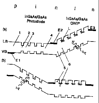
FIG. 2 shows in details a and b, the band diagrams
respectively of an advantageous preferred embodiment of
the invented two-color detector. The parallel continuous
lines represent the valance band (VB) and the conduction
CA 02232084 2003-05-28
8
band (CB), respectively. The layers with smaller band gaps
20 in the p-i-n photodiode structure correspond to the
InGaAs layer regions, whereas the layer regions with
larger band gaps contain GaAs. The i-layer designed in
this manner serves, in particular, to expand the
sensitivity range to wavelengths for which the GaAs
substrate is transparent. Regions with a larger band gap
21 in the QWIP structure correspond to the AlGaAs layer
(5), whereas the regions with smaller band gaps
respectively laying therebetween are composed of n-doped
GaAs.
The quantum well structure is dimensioned in such a manner
that the charge carriers L located in the potential wells
assume quantized states and that the barrier height
determined by the large band gap in the AlGaAs layers
prevent the charge carriers from tunnelling through from
one potential well to the other.
In FIG. 2(a) an external voltage applied via electrodes E1
and E3 causes the photodiode to operate in the forward
direction. Under these voltage conditions, the band
diagram of the QWIP structure is bent due to the extant
external electrical field in such a manner that, due to
optical excitation, the electrons located in the lower
subbands are excited into upper states (not shown) lying
near or above the conduction band edge. Due to the optical
excitation, charge carriers of this type can also be
partially raised into the continuum i.e., above the
conduction band edge energy so that they are immediately
drawn off laterally due to the external electrical field
and, in this manner, are able to contribute to the photo
current.
CA 02232084 2003-05-28
9
The operating state of the two-color detector according to
FIG. 2(a) represents a case in which the spectral
sensitivity range of the QWIP structure prevails, so that
the developing photo current is solely composed of charge
carriers emanating as a result of intersubband absorption
processes. If however, the external voltage is applied so
that the photodiode is biased in the reverse direction,
the charge carriers generated inside the i-layer are
separated due to the optical absorption by the electric
field prevailing within the i-layer and, in this manner,
contribute to the photo current.
An essential characteristic of the invented two-color
detector is that the noise behavior of the entire detector
is determined by that part of the detector in which the
photo current is generated. This is due in particular to
the fact that the photodiode biased in the block direction
has an extremely high dark resistance relative to the
differential intrinsic resistance of the QWIP structure,
so that the latter can be ignored. Likewise the
differential intrinsic resistance of the photodiode, which
is biased in the forward direction, has such a low value
that the noise portion from this detector region compared
to the noise portion of the actively operated QWIP
structure can be ignored due to an appropriate material
selection.
Preferably the two-color detector, as described in the
mentioned example according to FIG. 2 is optimized to two
wavelengths so that long wave radiation portions are
absorbed by the QWIP structure and the short wavelength
portions are absorbed by the p-i-n photodiode.
FIG. 3 is a diagram showing the dependence of the spectral
sensitivity of the two-color detector of FIG. 1 on the
CA 02232084 2003-05-28
photon energy, for two different voltage conditions. The
spectral sensitivity is shown in amperes per irradiated
photon power in watts along the ordinate. The photon
energies are plotted on the abscissa.
If the external voltage is 2 volts in the forward
direction of the photodiode, the spectral sensitivity of
the QWIP structure is 0.5 A/W at a photon energy of
153 meV. If, however, a bias voltage of 1 volt is applied
in the block direction of the photodiode, a spectral
sensitivity of 0.18 A/W at a photon energy of 1.47 eV is
yielded in the region of the photodiode.
The measured data generated by the invented two-color
detector correspond to the respective detector
sensitivities of separate known individual detectors.
Thus, it can be demonstrated that a combination of a
radiation detector composed of a photodiode and a quantum
well intersubband photodetector possesses similar
detection properties as single individual detectors do.
Furthermore, FIG: 3 shows in the right bottom part of the
diagram that by irradiating the two-color detector from
the back side (back illum.), i.e., from the side of the
base substrate, the sensitivity range breaks off at 1.5
eV, which can be explained by the great absorption of the
base substrate. In contrast, the dotted line indicates the
spectral sensitivity of the photodiode under forward
illumination which lies considerably above the value under
backside illumination.
In addition to the aforementioned preferred embodiments of
the invented two-color detector, other combinations of
materials or doping possibilities are feasible. Thus n-i-p
photodiodes can also be employed and can be combined with
CA 02232084 2003-05-28
11
a correspondingly p-doped quantum well structure. Likewise
inverted layer sequences are feasible in which first the
QWIP structure and then the layers of the photodiode are
precipitated onto the substrate. Additional preferred
embodiments are yielded, by way of illustration, when a
p-doped quantum well intersubband photodetector, i.e., a
QWIP structure having p-doped quantum well layers and a
p-conducting contact, are employed.
Moreover, there are alternatives to the above described
material system AlGaAs/GaAs/InGaAs. Thus, it is also
possible to precipitate onto an InP-substrate, the base
substrate, a multilayer sequence composed of InGaAs/InAlAs
as the QWIP structure adapted to the lattice constant of
the substrate crystal respectively slightly strained.
Furthermore, InGaAs can be selected as the photodiode
material.
Alternatively, a multilayer sequence composed of
GaSb/AlGaSb can be precipitated as the QWIP structure onto
a GaSb substrate on top of which InAs or a superlattice
composed of GaSb-InAs or composed of AlGaSb/InGaSb can be
precipitated as the photodiode layer.
By using different materials, and by a suitable selection
of layer parameters and types of doping, two-color
detectors can be conditioned as desired using the invented
combination of a photodiode and a QWIP structure. Thus,
the detector regions can be separately optimized for
different spectral sensitivity ranges respectively.
A diffraction grating applied onto or under the detector
structure usually employed in connection with QWIP
detectors is utilized as a further advantageous
improvement of the invented semiconductor heterostructure
CA 02232084 2003-05-28
12
radiation detector. The advantage of a grating of this
type is that, due to the polarization selection principles
for intersubband transitions, the incident light must have
a component of the electric field vector along the growth
direction of the semiconductor lattice. This means that
the propagation direction of the light within the detector
structure should occur perpendicular to respectively
diagonal to the growth direction. In order to meet this
demand better, the part of the radiation falling onto the
structure or the part of the radiation reflected opposite
the illuminated side of the detector, which lies in the
spectral sensitivity range of the quantum well
intersubband photodetector, are diffracted diagonal to the
incidence direction.
The invented two-color detectors can be operated in single
operation as well as in an array arrangement. Typical
lateral dimensions of a single detector are (10-1000pm)2
with a typical overall layer thickness of a few um. In
particular, two-color detectors of this type are employed
in so-called focal plane array camera systems which are,
by way of illustration, used in thermography.
The foregoing disclosure has been set forth merely to
illustrate the invention and is not intended to be
limiting. Since modifications of the disclosed embodiments
incorporating the spirit and substance of the invention
may occur to persons skilled in the art, the invention
should be construed to include everything within the scope
of the appended claims and equivalents thereof.