Note: Descriptions are shown in the official language in which they were submitted.
CA 0223261~ 1998-03-18
-- W O ~8/01~ PCT~B97/OU850 -
Dual tr~ncmitter arrangement with back-up switching
The invention relates to tr~ncmitter arrangements for multi-channel
operation, and more particularly to arrangements in which switch-over to a back-up
tr~ncmitfer is desirable.
To prevent direct revenue loss, and loss of subscriber or listener loyalty,
most commercial radio and television transmitter arrangements include some provision for
continued broadcasting even though a portion of the regular tr~ncmitter has failed.
~ometimes an entire duplicate transmitter and modulator are provided. However, such
10 arrangements are quite expensive, so a common arrangement includes a back-up transmitter
of less than half the power of the main tr~ncmit~er. Antenna connections and low level
signal inputs usually must be changed from one tr~ncmitter to the other, and the back-up
tr~ncmitt,or may require a significant warm-up time to provide stable operation. These make
automatic switch over difficult and cause an undesirably long service interruption.
According to the invention, a multi-channel transmitting arrangement
includes at least two tr~ncmittçrs, each of which in normal operation transmits a block of
signals for approxim~tt~ly half the total bandwidth to a communications device such as a
20 cable, waveguide or ~ntenn~ when the chalmels are similar, each transmits half the channels.
In the event of failure of one of the tr~ncmitt~rs, the signals for the block or channels it has
been tr~ncmitting are provided to the other transmitter, which then transmits all the channels.
Preferably the power tr~ncmitt~d per channel will remain substantially nnrh~n~ed, although it
may not be possible or practical to avoid an increase in distortion. Alternatively, the power
25 level per channel may be reduced.
In normal operation, one block of ch~nnel.c may occupy the lower half of
a band, and the other block occupies the upper half. An al~ellla~ive arrangement may use
two blocks with interleaved ch~nn.o.lc, where each block is spread over nearly the entire same
band.
- = -
CA 022326l~ l998-03-l8
~- W O 98/01~9 2 PCT~B97/00850 -
Because high level switching of antenna connections is not required, an
arrangement according to the invention is relatively easy tO aulomate, and no warm-up time
is lost.
Whenever, in normal operation, each tr~n~.nittt~r is operated below its
m~iml]m power output, for example to improve operating life or to reduce distortion, itiS
usually practicable that the back-up mode provide for tr~n~mi~cion at the same power level
per channel, so that service area coverage is not reduced. This is particularly applicable
when adaptive power control is used to vary the tr~mmitting power to accommodate time-
- varying changes in signal propagation over the service area, and the tr~ncmitrçrs may be
iO expected to be operating normally well below saturation.
In situations where signal attenuation in the service area fluctuates widely
over the course of a year, transmitter operating cost considerations may make it desirable to
operate the system such that, when minim~lm transmitter power will suffice, it is possible to
turn off or to put one transmitter in a standby mode, and to use the switch to transfer all
channels to the other tr~n~mitt~r. Where this mode is otherwise practicable, an important
consideration will be the time required to acl:ivate, warm up or stabilize the transmitter which
is not being actively used, so that high reliability of service can be m~3int~in~d.
In a preferred embodiment, the tr~n~mitting arrangement handles a
plurality of television or similar wide-band channels at frequencies above 10 to 12 GHz, such
as a 1 GHz band between 27.5 and 28.5 GHz. For output powers of 1~0 watts per block,
one traveling wave tube for each block of 25 FM channels provides sufficient power per
ch~nn,-l tO provide omnidirectional coverage out to a 3 mile radius. In normal operation, the
lower frequency tube transmits ch~nn~lc 1 - 25 at 27.5 to 28.0 GHz, and the upper tube
transmits channels 26-50 at 28.0 to 28.5 GHz.
In another embodiment, each tr~n~mitter includes a plurality of solid state
amplifying or mixing/amplifying devices connected to one or a like plurality of antenna
elements. Where each such device normally provides power for one small frequency block
or respective channel of a large number of ch~nnel~ being transmitted, under standby
operation each device would then transmit two such blocks or channels.
At some sacrifice in added complexity, the same inventive principle can
be applied in situations where it is desired to have more than two amplifiers h~n~lin~
respective portions of the spectrum, and in the event of failure or poor performance by one,
this portion can be shared among the others, or can be added in its entirety to the block
tr~n~mittPd by another.
CA 0223261F 1998-03-18
-- WO 98J0 1~1g 3 PCT/IB97/00850
Fig. 1 is a schematic diagram of a cellular tr~ncmitring arrangement in
accordance with the invention, and
Fig. 2 is a sch~m~tic diagram of a switching arrangement for use with
5 the invention.
The system shown schem~t~ ly in Fig. 1 includes tWO pluralities of
signal sources 10 and 11, which are respectively modulated and combined in modulators 20
10 and 21 to provide blocks of signals 22 and 23. ~;ach block of signals may include channels
of different types, modulation characteristics and individual bandwidth, or could be a single
broadband channel; it is not n~cÇC~ry that more than one signal source 10 or l l be involved.
In fact, the combined blocks 22 and 23 could represent one ~ery wide band program material
which, because of limit~tinns on tr~n~mitter or receiver technology, or some other reason, is
15 preferably tr~n~mitte-~ in two portions over respective tr,~ncmitters.
The signal blocks 22 and 23 are each input to a primary coupler 30 and a
standby coupler 31. These couplers are normally identi~al, and may be simple signal
combining devices or active devices such as frequency converters. Each coupler has two
outputs, one cont~inin~ signals corresponding to block 22, and the other cont~ining signals
20 corresponding to block 23. The four outputs are input to a switch 40, which would usually
be autom~tic~lly electrically controlled. The switch has two outputs, one providing signals to
transmitter 50 and the other to tran~mitt~r 51. Transmitter 50 has iL~. output fed to antenna
52, and transmitter 51 has its output fed to antenna 53. Of course, where it is
technologically feasible, the outputs of both tr~n~mitt~rs can be fed to one antenna, so long
25 as failure of one tr~n~mitter will not load the other because of coupling through the antenna
or its feed.
A control 6û is connected to sense loss of output from either of the
transmitters S0 and 51. The sensin$ is shown as coming from the respective antennae 52 and
53, but it will be clear that loss of tr~n~mitt~r output can be sensed at other locations within
30 the tr~n~mitter and feed combination, or remote from the antenna. The control 60 has an
output which is connected to cause operation of the switch 40.
In normal operation, switch 40 is set so that the output signals from
primary coupler 30 corresponding to block 22 are input to tr~n~mitter 50, and the output
signals from primary coupler 30 corresponding to block 23 are input to tran~mitter 51. In
CA 0223261~ 1998-03-18
-_ W O 98~ g 4 PCTnB97/00850 -
the event of loss of output from one of the tr~n~mTtters (or any other failLIre affecting output
from one only of the transmitters), the switch 40 is set to couple signals from the standby
coupler 31 to the tr~n~mitter whose output had been normal.
According to another feature of the invention, the control 60 can be
5 connecterl to an adaptive power control circuit, so that the adaptive power control circuit
provides the output loss signal to the control 60, or can use the tr~n~mitt;ng power control to
affect a change in output power per channel autom~tir~lly upon switching to the standby
mode. The adaptive power control circuit ~ay includes one or more sensors 70 provided at
- different locations within the tr~mmitt~r service area, which transmit by wire (e.g.,
10 telephone lines, or telemetry signals such as "carrier current" over local power lines) or
radio or other link tO a unit 72 at the transmitter site. The unit includes a control portion 74
which provides power control signals; and a receiver portion 76 which receives the radio or
other link signals from the sensor or sensors. The power level control is shown as being
performed at the tr~n~mitt~rs 50, 51. However, depending upon the choice of e~uipment and
15 modulation or frequency converting arrangement, it may be preferable to control tr~ncmittl~.r
power level by affecting circuits in the couplers 30, 31 or modulators 20, 21.
The sensors 70 can be provided at one or more predetermined, fi~ced
locations. Alternatively, some or all of the normal service receivers, such as customer
premises equipments, may be equipped for two-way operation. In that case the receiving
20 sections at those service receiving sites can be polled periodically to provide a report signal
related to the signal strength being received at the individual site. Where propagation is
affected heavily by rainfall, such a system provides a higher likelihood of identifying the
effect of small intense rain cells.
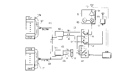
The switching arrangement shown in Fig. 2 is especially adapted for
25 tr~n~mi~ion of a large number of FM television channels having a nominal bandwidth of 20
MHZ each. Of course, one or more channels can have wider or narrower bandwidth, and
can carry digital or other signals at varying bit or burst rates. There is no need that the
number of ch~nn.~ or their spacing be the same for the two blocks.
Frequency agile motl~ tor bloc~cs 120 and 121 each contain 25 individual
30 modulators such as 120a, and take input signals (not shown) which may be baseband signals
o} may themselves be higher frequency signals such as ISDN or T-1 or E-1 signals, and
modulate them at different ~h~nnel frequencies. The outputs of modulator blocks 120, 121
are bloclcs of signals 122, 123 between 50 and ~50 MHZ, so that a total of 1 GHz of channel
space is being provided without need for modulators which will operate at or above 1 GHz.
CA 0223261~ 1998-03-18
~- W O 98~ G'~ ~ PCT~B97/00~50
Each of these blocks is input to a primary L-band upconverter 130 and a standby L-band
upconverter 131.
In this embodiment the two upconverters are identical. They have
respective outputs of two signal blocks 132, 134 and 133, 135. Blocks 132 and 133 contain
S signals between 2.1 G~Iz and 2.6 GHz, and blocks 134 and 135 contain signals between 2.6
GHz and 3. I GHz. The blocks 133 and 135 are then combined in a coupler 137 to form a
block between 2.1 GHz and 3.1 GHz, and provided to a common terminal of a single pole,
double throw coaxial switch 147 which is part of a three independent section electrically
controlled switch 140. For normal operation, over a normally closed contact set whose
common contact is connPctPd to a mixer 15~ of a tr~n~mitt~r 150, a switch section 142
connects the block 132 to the input of the tr~n~mitter 150; similarly, over a normally closed
contact set switch section 144 connects bloclc 134 to a transmitter 151.
In the event that tr~n~mittPr 151 is sensed to have improper or no output,
switch 142 is operated to connect the input tO mixer 154 to a normally open contact which in
turn is connected to a normally closed contact of switch 147, thereby providing the signals
forming blocks 133 and 135 to the mixer 154. At the same time, switch 144 is operated.
The normally open contact of switch 144 is connected to a normally open contact of switch
147, so that the input to tr~ncmitrpr 151 is hll~llu~d.
In the event that transmitter 150 is sensed to have improper or no output,
switch 144 is operated to connect the input to transmitter 151 to the normally open contact
which in turn is connected to the normally open contact of switch 147. Simultaneously,
switch 147 is operated to connect signals from the coupler 137 to its normally open contact,
thereby providing the signals forming blocks 133 and 135 to the transmitter 151. At the
same time, switch 142 is set to the normally open contact which is connected to the normally
closed contact of switch 147, so that the input to transmitter 150 is interrupted.
In this embodiment, tr~n~mitter 150 includes an oscillator 155 conn~ctPd
to the mixer 154, to upconvert the L-band IF signals to the 27.5 to 28.5 GHz band. The 28
GHz band signals are then amplified in a traveling wave tube amplifier 158 which is
connPctPfl to the antenna 152.
The inventive arrangement is usable whether or not transmitter distortion
cancellation techniques are included. Such techniques may, for example, include feed
ful wdld, or predistortion.
It will be noted that the preferred embodiment is optimized for
trancmi~sion over a 1 GHz continuous band. If frequencies allocated for service are not in
CA 022326l5 l998-03-l8
-- W 098~-~5-1~ 6 PCT~B97/008S0 -
one contiguous band, different variations may be ~lel~ d. For example, if transmission is
permitted from 27.5 to 28.35 G~Iz and from 29.1 to 29.25 GHz, and possibly also from 31
to 31.3 GHz, practical limit~tic-n~ on the equipment may requsre careful opt;mi7~tinn. For
example, it may be preferred, if only the two frequency bands below 30 GHz are utilized, to
S extend the IF band to a total of 1.75 GHz, and to leave a portion with no signal. This has
the advantage that only one upconversion is required, but it greatly widens the pass band
required for the rF. Alternatively, the modulators can be set to provide jUSt sufficient empty
band between those ch~nnPIc below 28.35 GHz and those above, so that sharp cut-off filters
in the tr~n~mitt~r can feed the lower blocks to one upconverter (mixer and oscillator) and the
10 upper block to another upconverter. The latter technique appears more suitable if the band
above 30 GHz is also to be utilized
Many other variations using the invention will become clear to those of
ordinary skill, upon reading this application. For example, the split band described above,
where three somewhat separated blocks of frequency are used, may be optimized by use of
IS more than two tr~ncmi~ting sections, and at some additional cost each, or selected ones, of
the transmitting sections may have filters or other circuits permitting transmission, when
operating in the back-up mode, at frequency bands separated from that normally transmitted.
It will be clear that different bands or channels may not only have different bandwidths, but
may contain markedly different signal types or be differently modulated. Although
20 undesirable from the standpoint of complexity, back-up operation in which the added block is
tr~n~mitt~d with a different polarization is also possible.
accordingly, the scope of the invention should be measured only by the appended claims.