Note: Descriptions are shown in the official language in which they were submitted.
CA 02232734 2003-02-24
WH-10 075CA
OPTICAL MODULATOR HAVING A REFLECTION
ELATE MOL'~T'rED ON A REFLECTION END WTTH
AN INCLINED ANGLE AGIANST T~-iE REFLECTION END
Background of , tlze,:Invent'_ic>n
This :.nvent~.or~. ralar_,es to an optical modulator using
a waveguide formed ~»~ a substrate exhibiting the elector-
optical Poc:kels eff:~~rt .
U.S. Patent No. 5,278,499 andJP-A-5 273260, disclose
an optical modulator which is used irn a device such as a
modulator or a device for optically rneasuxing an
electromagnetic field intensity, and which utilizes a
substrate of an elect~ro--optic crystal such as LiNb03 or
the like. In detai.:l, a waveguide of a branched
interferometer type is formed by Ti thermal diffusion on
the surface of the s2rbstrate. The waveguide has an
incident er..d at an end surface of the substrate,
extending to the opposite end surface of the substrate,
with two branched w;~.~reguide portions brarrc.hed at a
branched point and exposing their ends at the opposite
end surface. Modulating electrodes are formed on the
surface of the substrate in the vicinity of the
waveguide, and a light reflecting plate is fixedly
mounted on the oppo;a:i.t:e end surface of the substrate by
use of an .adhering ;agent of, for example, an ultraviolet
curing type.
In the optical modulator, a light beam is incident
into the incident end. of the wageguide at the end surface
of the modulator and propagates in the waveguide. The
light beam is split at. the branched point :into split
beams which, in turn, propagate through branched
waveguide portions <:;md then is :refl.ected as reflected
light beams by the .r.~eflecting plate. The reflected light
beams propagate backward in the branched waveguide
CA 02232734 2003-02-24
WH-10 075CA
,,
r
portions and are cc~~nb:ined at the branched portion, then
outgoing a.:~ an outs:wt= l~.ght from the incident end. Its
will be not:ed that the incident end is also used as a
light outgoing end. 'C.l~e intensify of the output light:
beam is changed by application of a voltage to the
modulating electrode" :The intensity change is dependent
on a trigcnometri.c :~1.AI'lCtion of the voltage applied and
has the maximum and the minimum.
The o.~~tlcal mo:~a.r:Lator_ has ar~ optical. bias point
which is determined as an intensity of the output light
when the a~~plied vo:Lt:age :is 2erc~. TLie opt.ic~al bias point
is present at the m,:zf~umum point ef <r trigonometric
function cL.rve of the: output .light intensity change if
the optical modulat::~z° coul_d be formed in a geometrically
symmetric form.
The o~tir.<~1 moc:lulat:or :is requir~e~d to have its
optical bias point :_rc:1-'pusted at: a middle point on a linear
portion between the maximum and the minimum of the
intensity change of t: rue output:. light.. Thus, the light.
beam is linear:Ly modulated by the voltage applied. On the
contrary, when the yt::ical. bias point is offset from the
middle point toward:: t'tue maximum or the minimum, the
intensity modulation linearity and sensitivity are
degraded.
Since it is vex-y difficult to adjust the optical
bias point by ~:~roce;::ase~s f_or producing the optical
modulator. Tlnis r~:_>c~,tzires high production accuracy, and
results in a law production yield.
Summary of the- Invention._
It is an object: c,~i_ this i.n~~~ention to provide an
optical moclulat:or wluose optical bias point is easy to
adjust and which therefore has excellent intensity
modulation linE~arit~,~~ a.nd sensitivity.
According to t}iis invent:ior~, there is provided an
CA 02232734 2003-02-24
WH-10 075CA
3 _
optical modulator c~~rnprising a substrate exhibiting an
electro-optical Pockets effect and having a first and a
second end surfaces opposite r_o each ether, an optical
waveguide of a branched interferometer type formed on the
substrate ~.nd havin~_~ a fz_rst anci a second branched
waveguide portions with an input end and a reflection
side end e:x:posed in >aid f=first: and second end surfaces
respectively, a modui.ating electrode formed on the
substrate in t:he vic::.nity of the branched :interferometer
type optical waveguide, and a reflection plate mounted on
the second end surf::~c~e, wherein the reflect:ion plate has
an inclination against the second end surface of the
substrate.
The optical modulator may preferably further
comprise a spacer d:i_~;posed between a side of said
reflection plate an~~l said second end surface of said
substrate to tlnereb~ for-rrc said incl.~nation and a space
between said second end surface and said reflection
plate.
In the optical modulator, the space is preferably
filled with an adhe;::>i ~~c:~ to adhe-r-e the secoxxd end surface,
the reflection plate and the spacer to each other.
Brief _-Descr-ipt:icn _of-the Drawings_
Fig. 1 i.s a scluEnm~.tic plan view of a mown optical
modulator;
Fig. ? is a scl:cematic plan view of an optical
modulator according to a first embodiment of this
invention;
Fig. :3 is a gr~.ph. showing a modulated intensity
curve in tlm~ optica:!. mod.ulato:r of FIG. l :ir~ r_omparison
with that :i_ n the opt: i cal madul_ato:r of FIG . 1 ; and
Fig. 4 is a schematic plan view of an optical
modulator according t.o a second embodiment of this
invention.
CA 02232734 2003-02-24
WH-10 075CA
Descri.~tion of._-the-Preferred Embodiments:
Prior to description of preferred embodiments of
this invention, desc~x-ipt~ion w:1:1 be made a:~ to a known
optical moo.ulator illustrated in FICi. 1 in order to
support the better ~.zrw~erst:and.ing of this invention.
Referring to Fig. 1, the known optical modulator 5
comprises a lithium niobate (~i~TbO<sub>3</sub>) substrate l on
which a waveguide 9 c>f a branched interferometer type is
formed by 'Ii thermal_ diffusion. The branched
interferometer type waveguide has two first and second
branched waveguid.e :~c:>z-tions 17. :end 1.3. On t:he substrate
7, a modulating elert.rode 15 is formed in the vicinity of
the waveguide 9 and oornpri.ses f~.rst, second and third
longitudinal e::Lectr~::~dE:e portions 17, 19 and 21 extending
in paralle:L wit=h th,~ waveguide 9, a first -_ateral
electrode portion 2.~ e::~tending From one side toward the
opposite side of th~=_. substrate 7 and in a direction
perpendicu:Lar to the first anti 1-:bird longitudinal
electrode portions l.7 and 21 and connected to an end of
each of th: fig=st a:nd. third lon<~itudinal electrode
portions 17 and 21, and a second lateral electrode
portion 25 extendinyt f~:~om the opposite sided toward the
one side of the sub:~t~:~ate and im a direction
perpendicular t:o thfe l.c~r~gitudin<xl second electrode
portion 19 and connfected to an c_>pposite end of the second
longitudinal electrode portion 19. Terminal_ pads 27 and
29 are formed apt thee terminal emds of the f:i.rst and the
second lata_ral elect..rade portions 23 and 25 at opposite
sides of the substrate 7, respectively.
The substrate '% has a light incident side end 31 and
a reflection side eruct surface 3;'s opposite to the light
incident s:ide end surface 31. On the reflection side end
surface 33, a light x.~ef:lectior7 ~:date 35 having a
reflecting surface 3'7 is adhered by, for example, an
CA 02232734 2003-02-24
baI-I-10 075CA
j
ultraviolet: light curing adhesive agent. The intensity of
the output light is measured by a light intensity
detector (not shown) connected to an end of the waveguide
9.
In the known optical modulator 5, when a light beam
or a laser propagat~~.~5 iro t: he waveguvc~e 9, :its intensity
is changed dependin~_on a trigoncmet.ric function by an
electric field due t:c:a a voltage app~_ied to the modulating
electrode 15, as is represented bye
Pout= . alpha . Pin { 1+c.~~~ ('J1 . mutt idot . . pi . /V . p:i . + . phi . )
} /2
(1) where Fout is o~,ztp~.zt 1_ight intensity, 1?in being
incident light inten~~~ity, V.pi. beirig a voltage
corresponding to a half period of the output light
intensity change der.~e=~ruciing on tie tz~igonometric function
of the applied voltage (which will be referred to as "1/2
wavelength voltage"), .al.pha. bE:eing a light: loss factor,
V1 being the applie~::~ voltage, amd .phi. being a phase
angle of the optical bias point shifted from the maximum
point when the appl:i.ed voltage is zero.
The known opti~~:al modulator 5 of FIG. 1 was produced
by forming a patter:u of Ti film with 40-100 nm thickness
on a lithi-am niobat~.~ ~~ubstrate '~ which was cut out in a
direction perpendic~_ilar to the X crystal axis, performing
the Ti diffusion at a t;emperat.ur_~e of 1,000-1,100. degree.
C. for 4-10 hours tc~ form the waveguide 9, and forming a
metallic pattez:w of the modulating electrode 15 in the
vicinity of- the braocch.ed wavegu:i.de portions 11 and 13.
Then, the -Light injection end surface 31 and the
reflection side end ~~uz.°face 33 c:~f th.e substrate 7 were
polished into a mirvc~r surface. On the reflection side
end surface 33, there was fixedly mounted a reflection
plate 35 which compl~i.ses a glass plate coated with a
metallic coating suc~~h as gold. '~'he produced optical
modulator c_>f the knc.:wn type had a width (w) o.f 6 mm, with
a distance ~~f 3 6 . ml.i . m. between the branched waveguide
CA 02232734 2003-02-24
wH-10 075CA
F -
portions. 7.'he produck:d optical modu::iator 5 was measured
in a characteristic of the output Eight responsive to the
voltage applied. The measured characteristic is shown at
a dotted line 43 in ~~ :ig . 3 .
Referring to F:ic~. 3, the known optical modulator has
an optical b:ias poia:~t: 45 at a positwon close to the
maximum of the output light intensit:y curve 43 and
V.pi.=5 V.
The known optical modulator however has the problems
as described in the F-3ackgx-oun.d of t:hE~ Invention.
Now, a.escription will be made as to an embodiment of
this invention with reference t~o Fic~~;. 2 and 3.
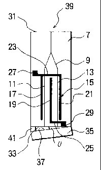
Referring to Fic~. 2, the optical modulator 39 shown,
therein comprises a ~su:k~strate 7 of 7 ithium niobate on
which a branched int~E.er.ferometer type waveguide 9 is
formed by Ti thermal diffusion, and a modulating
electrode :L5 dispos:~~:1 :iri the vi~~ini.ty of the waveguide 9
in the similar arrangement to the known opptical
modulator. A light i..r:.t:~=_nsity detector (not shown) is also
connected to an end c~f the waveguide 9 so as to measure
the intensity c>f an c.:~t.~t~.put lighT: thE~refrom.
The optical mo~~ii.rlator 39 is different from the known
optical mo~:3ulat:or i:u t.luat. a refl.ect.ian plate 35 having a
light reflection far~.e 37 is mounted on a light reflection
side end 33 of the ;:substrate 7 through a spacer 41 by
which the :reflectiorL ~~ide end surface 33 and the light
reflection face 37 make an angle .theta, therebetween.
The s~.zbstrate ~% , t:he ref le<rt ion plate 23 , and the
spacer 41 are fixed to each other by an adhesive agent
such as an ultx~avio:l.et curing adhesive agent. It is
preferable that the adrnesive agent is filled in a space
defined by the subs t:rat:e '7, the reflection plate 23, and
the spacer 41.
In detail, the spacer 41 is disposed between a side
of the ref:l.~action s=:.de end surface .',3 and a corresponding
CA 02232734 2003-02-24
WH-10 075CA
7 -
side of the light reflection face 37 and has a thickness
d so as tc~ make the. ~:~ngle . tl-~eta. . 'rYue thickness d is
given by the following c~quati.on:
d= (Va/V.pi . ) * ( .lambda. /4n) * (wjL) (2l
where Va i:~ an appl i_ec~ voltage :required to shift the
phase angle to the middle point when .theta.=0, .lambda.
being a wavelength «.f- the light, n being a refractive
index of the adhesiv;re agent, z~ being a distance between
the branched wavegu:ide portions, and w being a width of
the substr~.te. The ~cYhe~~ive agent i:~ prefe:rably one
having refractive index similar to the waveguide 9, for
example, n--1.48.
In the optical modulator 39, the split beams passing
through the branche~:~ waveguide port_ons 11 and 13 are
emitted from the sul:~~t::-ate 7 and ref_l.ected as the
reflected light beams by the light reflection face 37
into the branched w;:~wegui.de porl:ion; 1.1 and 13. The
reflected light beams ;,propagate backward in the branched
waveguide ~::ortions :_~. ;:~r.:d 13 anal thE~n combined into a
combined light beam at. the bran...ched point, which is
emitted as the outp:.it~ :Light . Due to the inclination angle
.theta. of the light: x-eflection faced 37, tYuere is a
difference of (Va/V.pi.)*(.lambda./~n) between optical
paths for frhe :split Y::~eams passing through t:he branched
waveguide portions v::o t:he light reflection face 37.
Therefore, the combl.n.ed light beam r~as an intensity
corresponding t:o th~>. middle point between t:he maximum and
the minimum when thc~ applied Vo_Ltage is zero. That is,
the optical bias po::~.r~t is adjusted to the middle point.
Now, she optic<xl modulator of F'ig. 2 will be
described .in connect: ion with it;~ prcduction method and
its modulation characteristic.
An optical modmlator shown in Fig. 2 according to a
first embodimernt of this invention was produced in the
producing manner similar to the known modulator of Fig. 1
CA 02232734 2003-02-24
WH-10 075CA
_. g _
as described above. After the reflewtion side end surface
33 of the :substrate 7 was polished, a reflection plate 35
was fixedly mounted on the reflection side end surface 33
with a spacer 41 of ,x thickness of LC, .rnu.m being
disposed between a side portion of the reflection plate
35 and the reflec:ti.on side end surface 33 so that the
reflection. plate 35 ::.s inclined aga=inst the reflection
side end surface 33. 'Che optical adhesive agent is filled
within a s~>ace defined by the reflec;t:ion side end surface
33, the reflection :surface 37 and. tl~e spacer 41. The
thickness ~c~f the sp~:xa:e.r 47_ was selected to adjust the
bias point into the optimum point as determined by
equation (2 ) describe=.c~ above .
Vlith respect to the optical. modulator 39 as
produced, a charact.~~:~ist.i.c: of the output Eight responsive
to the voltage applied was measured and is shown in Fig.
3.
Referring to Fig. 3, the optical modulator 39 of the
present invent~~on h<:~:-<:~ bias f~oint pat a middle point
between the maximum and the minimum ef a light intensity
curve 47 responsive t:c> the appl.ed voltage variation.
Referring to F:i_g. 4, an optical modulator 31
according to a secomci. embodiment= of this iruvention shown
therein comprises a ti.t:anium niobate substrate 7 on which
a pair of waveguide,::> 9 and. 53 of a branched
interferometer type i~, formed b~. Ti thermal. diffusion.
The waveguide 9 has fix:st and second branched waveguide
portions 1:L and 55 <-:nd. the otheo~ waveguide 53 has also
has first and second branched waveguide portions 13 and
57 which a:re connected to the branched first and second
waveguide portions .11 and 55, respectively, at the
reflection side end surface 33. A modulating electrode 59
is formed in the vi<: ini.ty of ~he branched waveguide
portions 1;L, 55, 13 and 57. The modulating electrode 59
comprises first thr<ugh fourth longitudinal electrode
CA 02232734 2003-02-24
WH-10 075CA
portions 6~_, 63, 65 and 67 extending along and over the
branched w~~veguide ;~o:rt:i ons 1. l , 55 , l;'s and 5 l' ,
respectivea.y. The rru~d~.x:Lat:ing electrode 59 has a first
lateral electrode portion 69 which e=xtends from one side
of the sub~~trate tc~,aard the other s:ide in a direction
perpendicular to the :longitudinal e_Lectrade portions and
is connected to one ends of the first and third elect=rode
portions 61. and 65. "_Che modul.atir~g electrode 59 further
has a second lateral eler_trode port=ion 71 "which extends
toward the one side r:o:. the substrate from the other side
in a direction perpendicular to the longitudinal
electrode ,abortions :;.end is connected t=o the opposite ends
of the second and fourth electrode portions 63 and 67.
Terminal pads '73 ancx "'15 ar-e formed at. a terminal end of
the first lateral electrode portion 69 at the one side of
the substrate 7 and at a terminal end of the second
lateral electrode p::~rt;.i.c>n. 71 at the c>ther ride,
respectively.
A reflection p'~at:c.~ 35 having a light :reflection face
37 is also fixedly mounted on a reflection side end
surface 33 of the sn.zbstrat.e 7 byr means of an adhesive
agent such as an ult:z:~aviolet curing adhesive with a
spacer 41 held between the light reflection face 37 and
the reflection side enc~i surface 33 to therE:~by form an
inclination angle .:.ret:.a. of the light ref-~ection face 37
against the ref_lectvi_c:~n side end surface 3.3.. The
inclination angle . L:lLet~.a. is also determined by d
according to equati~:~r~. ;2) .
In the above mfern.t.ioned embc:~diments, the substrate 7
has been described <:~s being made of lithium niobate.
However, the substra::~t: a can be made of any other material
having the electro-<_>ptical Pockets effect, such as,
lithium tantalite, 1=~L~~~~C', GaBs, and InP. As a method for
forming the waveguicle, moreover, the epitaxial growth
method or t; he proto:u exchange mc~tnod can be used in place
CA 02232734 2003-02-24
V~IH-10 075CA
- 1.0 -
of Ti thermal diffusion.
Still further, j~he spacer can be made of any
insulatable material having the thickness d, and is
preferably made of a:::.~.zrn_ina.
Although various preferred embodiments of the
present invent ion h:x,,~e been described here in in detail ,
it will be appreciated by those skirled in the art, that
variations may be m~:~r.:~e thereto without departing from the
spirit of the invention or the scope of the appended
claims.