Note: Descriptions are shown in the official language in which they were submitted.
' " CA 02232843 1998-06-18
- 1 -
PLASTIC PACKAGE, SEMICONDUCTOR DEVICE,
AND METHOD OF MANUFACTURING PLASTIC PACKAGE
BACKGROUND OF THE INVENTION
1. Field of the invention
This invention relates to a plastic package for
packaging a element, e.g. IC, CCD (charge coupled
device). More particularly, to a plastic package
possessing excellent moisture resistance.
2. Description of the Related Art
A resin package is used for packaging a chip in a
semiconductor device. A hollow package comprises a box
molded product made of plastic with a lead inserted
therein, a semiconductor chip is secured to the internal
bottom of the molded product, and a transparent or
semitransparent cover called "lid" is used to seal an
upper opening of the molded product, thereby fabricating
a semiconductor device. This hollow package is a type
of plastic package.
Semiconductor devises are used by incorporating it
into electronic products such as a video camera.
Therefore, strict moisture resistance is required for
such a semiconductor device so that a semiconductor chip
stored in electronic products always works in a normal
manner. For that, the hollow package which corresponds
to a container in a semiconductor device necessarily has
excellent moisture resistance for a long period of time
CA 02232843 2001-06-08
- 2 -
such that it can with:~i~and a severe test such as a
pressure cooker test.
Improvements in plastic compositions constituting the
resin package body have been made to raise the level of
the moisture resistance of the hollow package. For
instance, there has been a trial to convert the chemical
structure of an epoxy resin to various modified struct:ures
from the basic struc''ur_es such as a Novolak° type,
bisphenol type, or the like. However, this trial
unnecessarily satisfies improvements in the moisture
resistance. Also, other ingredients constituting the
plastic composition, f-or example, a mold release agent: for
improving the releasability from a metal mold and various
fillers added to control the coefficient of thermal
expansion and the heat. conductivity can insufficiently
contribute to the improvement in the moisture resistance
of the hollow package even if the sorts or amounts of
these are adjusted.
In order to solve these problems, a trial is made in
Japanese Patent Appl:ic:ation :Laid-Open (JP-A) No. 8-55927
which describes "As a result of various studies to improve
the moisture resistance of a hollow package, it has been
found that there is the cause controlling the moisture
resistance of the hol~_ow package in the condition of the
boundary between a lead and a plastic layer. Specifically,
it was clarified that a hollow package which has
adhesiveness between t;he lead and the
CA 02232843 1998-06-18
- 3 -
plastic layer can be obtained with an increase in
moisture resistance in long time use". Based on these
fact, Japanese Patent Application Laid-Open (JP-A) No.
8-55927 discloses a hollow package comprising a plastic
package body having a concave portion for storing a
chip; and a lead including one end extending to the
concave portion, the other end protruding from the
package body, and an intermediate portion embedded in
the package body, the one end being electrically
connected with the semiconductor element, wherein the
intermediate portion of the lead is formed so as to have
a roughened face. This structure results in achieving a
relatively long durability in terms of a durable time in
pressure cooker test as long as 14 hours.
The rough face is formed in the intermediate
portion of the lead by a sand blast method in which the
intermediate portion of the lead is processed by air
blast using alumina micropowder to form a rough face on
the lead.
Such a sand blast method for forming the rough face
on the lead, however, has the problem that it requires
troublesome operations for sufficiently removing alumina
micropowder attached to the surface of the lead. This
method also has the drawback of non-uniformity of the
roughened face condition caused by the accumulation of
polished powder on the surface of a metal mask used for
a lead frame. Further, this method imparts cost
CA 02232843 1998-06-18
- 4 -
problems including a great cost of expendable supplies
such as a metal mask for lead frame, alumina polishing
powder, and the like and a great maintenance cost
associated with the troubles of a sand blast apparatus
S itself, a compressor, or the like caused by the
polishing powder.
On the other hand, there is a greatly increased
demand for the provision of the moisture resistance of
the hollow package in a semiconductor device including a
CCD. It is required in practice to achieve an increase
in durable time in a pressure cooker test. It is also
required to develop a new process for manufacturing an
inexpensive hollow package having excellent moisture
resistance since there are exacting demands of a more
inexpensive hollow package.
SUMMARY OF THE INVENTION
It is an object of the present invention to provide
a plastic package which is inexpensive and is improved
in moisture resistance.
According to a first aspect of the present
invention, there is provided a plastic package
comprising: a plastic package body for storing a chip; a
lead member having one end extending to the inside of
the package body, the other end protruding from the
package body, and an intermediate portion embedded in
the package body, the one end being to be electrically
CA 02232843 1998-06-18
- 5 -
connected with the chip; and an oxide layer formed on a
part of the surface of the intermediate portion in the
lead member so as to have a thickness greater than
thickness of an oxide layer formed on the remainder part
of the lead member.
The use of the plastic package having such a
structure allows the adhesion between the lead member
and the plastic package body to be improved, whereby a
plastic package having a higher moisture resistance than
that of conventional plastic packages can be provided.
According to another aspect of the present
invention, there is provided a resin package comprising:
a plastic package body for storing a chip; a lead
member having one end extending to the inside of the
package body, the other end protruding from the package
body, an intermediate portion embedded in the package
body, the one end being to be electrically connected
with the semiconductor chip; and an irregular portion
having cyclical irregularities formed at a pitch of 10
to 100 um on the surface of the intermediate portion of
the lead member, the irregular portion having a length
of 0.1 mm or more in a longitudinal direction of the
lead member.
In this structure in which an irregular portion is
formed on the surface of the intermediate layer of the
lead member, the adhesion between the lead member and
the plastic package body is improved, which ensures the
CA 02232843 1998-06-18
- 6 -
provision of a plastic package having a more excellent
moisture resistance than those of conventional plastic
packages.
According to a further aspect of the present
invention, there is provided a semiconductor device
comprising a chip stored in the plastic package of the
types described above.
A semiconductor device having a higher moisture
resistance than that of conventional plastic packages
can be provided by adopting such a structure. Here,
solid state imaging devices are preferably used as the
chip and, among these, a CCD is preferable.
According to a still further aspect of the present
invention, there is provided a process for manufacturing
a plastic package comprising: a step of irradiating
pulsed laser beams to an intermediate portion of a lead
member of which one end is to be electrically connected
with a chip, while it is scanned, to form an oxide layer
on the intermediate portion of the lead member; and a
step of molding the lead member and a plastic
monolithically to make the intermediate portion of the
lead member buried in the plastic while externally
protruding the other end of the lead member from the
plastic.
If the plastic package is manufactured by such a
process, only a portion required to be treated is
selectively treated without providing the masking or the
CA 02232843 1998-06-18
_ 7 _
like on the subject in a different way from the sand
blast method, thereby enabling a manufacturing process
to be more simplified than conventional processes.
BRIEF DESCRIPTION OF THE DRAWINGS
Other objects and advantages of the present
invention will become apparent during the following
discussion conjunction with the accompanying drawings,
in which:
Fig. 1 is a schematically sectional view showing an
example of a plastic package of an embodiment according
to the present invention;
Fig. 2 is a schematically top plan view of the
plastic package of an embodiment according to the
present invention;
Fig. 3 is a schematically top plan view of a lead
constituting a part of the plastic package of an
embodiment according to the present invention;
Fig. 4 is a top plan view of a metal plate used in
a preliminary test of examples;
Fig. 5 is a top plan view of a metal mold for
manufacturing a test specimen used in a preliminary test
of examples; and
Fig. 6 is a graph showing a result of the Q
switch-frequency dependency of pull-out adhesion in
examples.
CA 02232843 1998-06-18
_ g _
DETAILED DESCRIPTION OF THE PREFERRED EMBODIMENT
The present invention will now be explained in
detail with reference to the drawings.
The plastic package of the present invention
comprises a plastic package body for storing a
semiconductor chip and a lead which is to be
electrically connected with each electrode of the
semiconductor chip.
(1) Structure of a plastic package
As the plastic package, those having a structure of
a lead mounting system or a surface mounting system may
be used. However, the present invention has the most
effect on a structure called a hollow package comprising
a plastic package body having a cavity and leads molded
monolithically with the plastic package body.
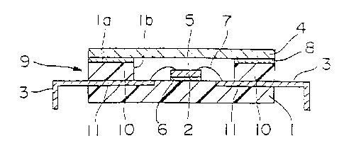
Fig. 1 is a schematically sectional view showing an
example of a plastic package of an embodiment according
to the present invention. A plastic package 9 comprises
a box plastic package body 1 and a lead 3 (a lead
member). A chip is stored in the plastic package and a
lid is used to close the plastic package and thereby to
manufacture a semiconductor device in which the
semiconductor chip is sealed in the plastic package. In
the concrete, the plastic package body 1 is provided
with a concave portion 5 for storing the semiconductor
chip 2 in the center thereof. The chip 2 is secured
within the concave portion 5 using an adhesive 6. Each
CA 02232843 1998-06-18
- 9 -
electrode (not shown) of the chip 2 is electrically
connected with the lead 3 via a bonding wire 7. A lid 4
is secured to the upper surface la of the plastic
package body 1 to close an upper opening lb of the
plastic package body 1. The lead 3 is integrated with
the plastic package body 1 to form a molded product as
the plastic package of the present invention.
There are no limitations to a process for
manufacturing such a plastic package. For example, the
plastic package body 1 can be produced by transfer
molding or injection molding. At this time, the lead 3
is inserted into a metal mold in advance prior to the
molding and plastic is then injected and cured or
solidified to produce a plastic package.
Fig. 2 is a top plan view of a plastic package 9
viewed from the side of the upper opening lb. The lead
3 is embedded into the plastic package body l, one end
(an inner lead 3a) of the lead 3 extends to the inside
of the plastic package body and is to be electrically
connected with the chip 2, and the other end of the lead
3 (an outer lead 3b) to be externally connected
protrudes from the plastic package body 1 and is
exposed. In this condition, an intermediate portion 11
defined between the inner lead 3a and the outer lead 3b
is embedded into the plastic package body 1,
specifically, a plastic layer 10 constituting the
plastic package body 1.
CA 02232843 1998-06-18
- 10 -
Accordingly, the intermediate portion 11 of the
lead 3 is secured within the plastic layer 10 whereby
the lead 3 is secured with the position thereof being
fixed. Then, the lead 3 is electrically connected with
the chip 2 via the inner lead 3a.
(2) Plastic package body
Examples of materials used as the structure of the
resin package body 1 include heat curable resins such as
an epoxy resin, polyimide resin, phenol resin,
unsaturated polyester resin, silicone resin, and the
like or heat resistant thermoplastic resins such as a
liquid crystal polymer, polyphenylene oxide,
polyphenylene sulfide (PPS) resin, polysulfone,
polyamide/imide, polyarylsulfone resin, and the like.
Among these, an epoxy resin, polyimide resin, PPS, and
the like are preferable.
An inorganic filler such as alumina powder, silica
powder, silicon nitride powder, boron nitride powder,
titanium oxide powder, silicon carbonate powder, glass
fiber, alumina fiber, or the like may be added to each
of these heat resistant resins. Other than the
inorganic filler, other additives such as a curing
agent, hardening accelerator, coupling agent, and the
like may be included, if necessary.
(3) Lead
Examples of materials used as the lead 3 include
iron-based alloys such as an iron-nickel, e.g. 42 alloy,
CA 02232843 1998-06-18
- 11 -
iron-nickel-chrome, iron-nickel-cobalt, and the like, or
copper-based alloys containing several metals selected
from the group consisting of magnesium, silicon,
phosphorus, titanium, chromium, nickel, zinc, tin, and
zirconium. Resides, metals or alloys ordinary used as a
lead material may be used.
The present invention is featured in that, in the
lead 3, at least a part of the portion adhering to the
plastic package body 1 is formed with an oxide layer or
an irregular portion having cyclic irregularities formed
at a pitch of 10 to 100 um. The oxide layer and the
irregular portion and methods for forming these will be
explained.
Fig. 3 is a top plan view of the lead 3. In Fig.
3, an oxide layer lla is formed on the surface of the
intermediate portion 11 of the lead 3, specifically at
the portion adhering to the plastic layer. The oxide
layer lla is required to be formed on at least a part of
the intermediate portion 11 of the lead 3. As shown in
Fig. 3, it is desirable that the oxide layer lla be
formed along the lengthy side of the box plastic package
body 1 so as to traverse the intermediate portion 11 of
each lead. The oxide layer lla is formed on the
intermediate portion 11 of the lead 3 in this manner,
whereby the lead 3 is firmly fixed to the plastic.
Thus, an admission passage for water through the
boundary between the lead and the plastic can be
CA 02232843 1998-06-18
- 12 -
perfectly shut.
The oxide layer must be formed on at least a part
of the surface of the intermediate portion 11 of the
lead 3. In this case, the oxide layer may be formed
S either on one or both of the surfaces of the lead 3
though the provision of the oxide layer formed on the
both surfaces imparts a more excellent moisture
resistant effect.
If, portions other than the intermediate portion 11
of the lead 3, specifically, the inner lead 3a to be
wire-bonded with the chip 2 or the outer lead 3b to be
connected with an external circuit is intentionally
formed with an oxide layer, a burr is stuck to the
surface of the inner lead 3a or outer lead 3b when the
plastic package body 1 is molded. In this case, the
burr can be perfectly removed only with difficulty even
in the succeeding washing step whereby there is the case
where the bonding force with the bonding wire 7 or other
wires is decreased. Therefore, it is desirable that
only the intermediate portion 11 of the lead 3 be formed
with an oxide layer.
Here, the oxide layer means a layer composed of an
oxide of a metal or non-metal and having a thickness of
the fixed order or more and there are no limitations to
the oxide layer except that it is obtained by the
treatment on the surface of the lead. It is noted that
the oxide layer does not include a surface oxide layer
CA 02232843 1998-06-18
- 13 -
formed by natural oxidation of a metal constituting the
lead (this surface oxide layer is hereinafter called "a
natural oxide layer").
As a material used for the oxide layer, it is
desirable to use a metal oxide prepared from at least
one of metal materials forming the lead 3. Such a metal
oxide is, specifically, prepared by oxidizing the
surface of the lead 3. Illustrating specific examples
of such a metal oxide, the oxide is iron oxide and/or
nickel oxide in case of using a 42 alloy as a material
of the lead 3. An oxide of other metals or non-metals
which are chemically stable and highly adhesive to a
material used for the lead may be used. It is
particularly preferable to use iron oxide as the oxide
layer.
The thickness of the oxide layer is not required to
be uniform. The thickness of at least a part of the
oxide layer is preferably from 5 to 500 nm and more
preferably from 10 to 500 nm. When the thickness is in
a range from 50 to 500 nm, the highest effect of the
present invention can be imparted. It is also desirable
that at least one position of the oxide layer of the
intermediate portion has a thickness of 1.5 to 500 times
that of a natural oxide layer formed on the surfaces
other than the intermediate portion. The oxide layer is
desirable to be formed from one edge to the other edge
of the lead in a direction transversely to the
CA 02232843 1998-06-18
- 14 -
intermediate portion of the lead. And it is also
desirable that the oxide layer is formed with a length
of O.lmm or more in the longitudinal directions of the
lead. But, the oxide layer should not always be formed
on the whole area above described.
It is considered that at least a part of the surface of
the lead is formed with the oxide layer having the above
thickness to improve the adhesion between the lead and
the plastic though the true reason has not been
clarified.
If the oxide layer is further provided with
microparticles of a metal oxide with a particle diameter
of 10 nm to 2 um on the surface thereof, the oxide
microparticle acts as an anchor to improve the adhesion
between the lead and the plastic. Also, the particle
diameter of the oxide microparticles is desirably from
50nm to 1 um.
As a method for forming the oxide layer on the
lead, a thermal method including laser irradiation,
electron beam irradiation, plasma processing, high
frequency induction heating, electric discharge
machining, flame treatment, or the like can be used.
Other methods including PVD (physical vapor deposition)
and CVD (chemical vapor deposition) may be used to form
the oxide layer on the surface of the lead though the
above thermal method is suitable in view of ease of the
steps of manufacturing the plastic package. Since the
CA 02232843 1998-06-18
- 15 -
lead has a figure of an extremely thin plate with a
thickness of 0.1 to 0.3 mm and is formed of a material
of an iron alloy or copper alloy, it is important that
the heat input by heat treatment is reduced to decrease
a warp of the lead. Therefore, it is effective to use a
high density heat source, e.g. laser irradiation.
Incidentally, in the case where the oxide layer is
formed on the surface of the lead by laser irradiation,
it is considered that microparticles of metal oxide
formed through the evaporation and scatter of a metal
material forming the lead will be accumulated on and
stuck to the portion exposed to laser beam on the lead.
The intermediate portion 11 of the lead 3 shown in
Fig. 3 may be formed with an irregular portion having
cyclic irregularities formed in one direction at a pitch
of 10 to 100 pm instead of the oxide layer. The
irregular portion can be prepared by roughly processing
the surface of the lead so as to provide the surface
with cyclic irregularities. When the intermediate
portion of the lead is formed with such an irregular
portion, the adhesion between the lead and the plastic
is improved due to an anchor effect. The pitch and the
surface roughness (R,~aX) of the irregular portion are
considered to contribute to the adhesion between the
lead and the resin.
It is more desirable that the pitch of the
irregular portion be from 25 to 100 um. The R~~~x is
CA 02232843 1998-06-18
- 16 -
desirably in a range from 1 to 100 um. The maximum
effect can be obtained when the pitch is in a range from
30 to 50 um and the Rmax is in a range from 3 to 20 um.
The irregular portion is required to be formed with a
length of 0.1 mm in a longitudinal direction of the lead
3 on one of the surfaces of the intermediate portion 11
of the lead 3. And the irregular portion is desirable
to be formed from one edge to the other edge of the lead
in a direction transversely to the intermediate portion
11. If the irregular portion is formed on both surfaces
of the lead 3, a more increased effect can be obtained.
Methods in which the lead 3 is treated by laser
irradiation or etching are exemplified as the method for
forming the irregular portion on the lead 3. Laser
irradiation on the lead 3 is suitable in view of ease of
the process of manufacturing the plastic package.
It is noted that both of the aforementioned surface
oxide layer and irregular portion may be formed on the
intermediate portion 11 of the lead 3. For example, an
oxide layer with a thickness of 5 to 500 nm may be
further formed on the irregular portion formed on the
intermediate portion 11.
When the oxide layer and/or the irregular portion
is formed on the surface of the lead 3 made of an
iron-based alloy of an extremely thin plate shape or the
like by laser irradiation, it is desirable to use laser
radiation at wavelengths ranging within the wave length
CA 02232843 1998-06-18
- 17 -
band of near infrared radiation. As the laser radiation
of wavelengths corresponding to those of near infrared
radiation, which can maintain the shape of the lead and
form an oxide layer on the lead, solid-state laser, e.g.
alexandrite, YAG may be used.
The wavelength of the laser radiation, which lies
in the wavelength band of near infrared radiation, is
desirably near 1 um which allows the laser radiation to
be decreased in energy reflectance of a metal and
increased in energy absorption rate. If pulsed laser
radiation is used as such a laser radiation, cyclic
irregularities can be easily formed in one direction.
Laser radiation having a wavelength of 1.06 um emitted
from Q-switched Nd:YAG laser is most suitable to satisfy
these requirements. When Q switch-type Nd:YAG laser is
used, the power range, which allows an oxide layer to be
formed on the lead without deformation of the lead, is
preferably from 15W to 50W at a working spot. A
desirable frequency of Q switch is in a range from 2 to
20 kHz, preferably from 2 to 8 kHz, and more preferably
from 4 to 7 kHz so that laser radiation is emitted in a
stable manner and the adhesion between the lead and the
plastic is improved. The surface of the lead is
irradiated with laser beams in these conditions whereby
an oxide layer as well as an irregular portion can be
formed on the surface of the lead and hence more
desirable effect can be obtained.
CA 02232843 1998-06-18
- 18 -
If a galvanomiller-scanning method using a f-a
lens-system is used for aligning laser beam when laser
radiation is applied, the surface oxide layer and/or the
irregular portion can be easily formed on only necessary
positions of the lead surface. For example, the pulsed
laser beam with the spot size of 80um on the irradiated
portion irradiates the surface of the lead while
scanning across the intermediate portion of the lead in
the above mentioned frequency. Then, the laser beam
irradiates another part of the lead at intervals of
O.lmm through 0.5mm from the already irradiated part.
This operation is repeated for several times until the
intermediate portion of the lead to be irradiated is
fully irradiated. Thus, irradiated lines are obtained
on the part where the pulsed laser beams are irradiated.
The number of repeating time of the operation may be one
or more, and the number becomes larger, the effect of
the invention becomes larger. Therefore, processes and
jigs, which are required in the conventional sandblast
method, specifically, pretreatment for masking, in
advance, the portions (inner lead 3a, outer lead 3b, and
the like) which is not required to be roughly processed
and jigs used in the pretreatment are unnecessary at all
thereby saving costs of expendable supplies.
EXAMPLES
A preliminary test was performed in advance
CA 02232843 1998-06-18
- 19 -
according to the following method to examine the effects
of an oxide layer and irregular portion formed on a
lead.
(Experiment 1)
Firstly as shown in Fig. 4, a metal plate 14, made
of a 42 alloy having a thickness of 0.25 mm with a
projecting strip 14b with a narrow width projecting from
one end of a rectangular base 14a, was surface-treated
in varied conditions to prepare four types of metal
plate. The surface treatment was performed on an almost
entire of both the surface of the projecting strip 14b
according to the following methods.
Surface treating method A: the sample was
irradiated with laser beams from a Q-switched YAG laser
irradiation apparatus, which delivered a rated power of
50 W, in the following conditions: wave length: 1.06 Vim,
frequency of Q switch: 6 kHz, beam scanning velocity:
200 mm/sec, aperture: fully opened, laser power at the
position 100 mm below the working spot: 22.2 W, and spot
size on the irradiated portion: 80 um. The laser
irradiation is applied by beam scanning on the
projecting strip 14b at intervals of 0.15mm until the
portion to be treated in the projecting strip 14b is
fully irradiated.
Surface treating method B: the sample was
air-blasted using a sandblast apparatus by blowing
alumina powder having an average particle diameter of 14
CA 02232843 1998-06-18
- 20 -
um from a nozzle having a diameter of 3.0 mm under an
air pressure of 5 Kg/cmzG at a feed rate of 18 mm/sec.
Surface treating method C: the sample was
irradiated with laser beam from a Q-switched YAG laser
irradiation apparatus, which delivered a rated power of
50 W, in the following conditions: wave length: 1.06 um,
frequency of Q switch: 12 kHz, beam scanning velocity:
200 mm/sec, aperture: fully opened, laser power at the
position 100 mm below the working spot: 22.2 W, and spot
size on the irradiated portion: 80 um. The laser
irradiation is applied by beam scanning on the
projecting strip 14b at intervals of 0.15mm until the
portion to be treated in the projecting strip 14b is
fully irradiated.
Surface treating method D: no treatment.
Next, the top ends of the projecting strips 14b of
the metal plates 14 respectively treated by the above
surface treating methods A to D were inserted into a
metal mold 12 for preparing a specimen used in a
pull-out test and were molded using a transfer molding
machine by injecting an epoxy resin and pressing at 165°
C under a pressure of 120 Kg/cm~ for two minutes. The
resulting molded products were used as test specimens.
The pull-out adhesion (Kg) between the metal plate
and the epoxy resin layer was measured using a tensile
tester (Tensilon UCT-5T) at a tension speed of 5 mm/min.
Five samples every test specimen were evaluated to
CA 02232843 1998-06-18
- 21 -
determine an average adhesion of five samples as the
pull-out adhesion of the test specimen. A dimension of
one surface of embedded parts of the each projecting
strip 14b is 4mm width and 5mm length in the test
direction. The results are shown in Table 1.
As shown in Table 1, a result was obtained in which
the test specimen treated by the surface treating method
A (hereinafter simply abbreviated as "test specimen A",
similarly in cases of surface treating methods B to D)
exhibited the highest pull-out adhesion. As for the
test specimen C, the same pull-out adhesion as that of
the test specimen B could be obtained. Therefore, it
was confirmed that the surface treatment of the lead
using laser radiation was effective.
Table 1
Surface ~ I ~~ I
treating A B C I D ~~,
eethodi
I
~ i
Pull-out
adhesion 3 2. 1 4. 1 3. 5 i 4.
(Kg) 0 8 1 I
(Experiment 2)
A lead frame plate, in which twelve leads 3 shown
in Fig. 3 were connected each other, was prepared and
both surfaces of the intermediate portion 11 of each of
leads 3 were treated by the same treating methods A to D
as in Experiment 1. In the surface treating method B,
CA 02232843 1998-06-18
- 22 -
the inner lead 3a and the outer lead 3b were masked with
a jig or a seal tape and the exposed intermediate
portion 11 was treated by sandblast. In the surface
treating methods A and C, only the intermediate portion
11 was irradiated with laser radiation by means of laser
beam scanning. Then, the lead frame treated by the
surface treating methods A to D was molded using a
transfer molding equipment to obtain a hollow plastic
package made of an epoxy resin shown in Fig. 2. This
plastic package was covered and sealed with a glass lid
using an epoxy resin adhesive and was subjected to a
pressure cooker test. In the pressure cooker test, the
sample was allowed to stand in a steamy atmosphere at
121°C under an humidity of 1000 for a prescribed period
of time and was then placed in a thermostat at 25°C for
30 minutes to observe the occurrence of clouding on the
glass lid. The number of samples was 10 and an average
time passage until clouding occurred was defined as a
durable time. The results are shown in Table 2. The
moisture resistance was determined as better with an
increase in durable time.
Similarly to Experiment 1, the best result was
obtained in the surface treating method A and, in the
surface treating method C, the same result as in the
sandblast method (surface treating method B) was
obtained.
CA 02232843 1998-06-18
- 23 -
Table Z
!Jurface '
.treating methods A i B ; C ~ D
i
Durable time
(hrs) j20. 1 ~14. 0'1 3. 21 4. 3~~
(Experiment 3)
The test specimen (see Fig. 5) used in Experiment 1
was surface-treated at varied frequencies of the Q
switch to examine the Q switch frequency dependency of
the pull-out adhesion. An average value of five samples
was defined as the pull-out adhesion of the test
specimen. The results are shown in Fig. 6. The
pull-out adhesion as well as the durable time largely
varied above the borderline of a frequency of 6 to 8 kHz
and it was confirmed that the durable time was best at
frequencies 7 kHz or less.
(Experiment 4)
The relation between an adherent oxide generated by
laser radiation and the pull-out adhesion was examined.
In order to prepare a sample having no adherent oxide, a
test specimen irradiated with laser radiation at a Q-
switch frequency of 6 kHz was sufficiently washed using
an ultrasonic cleaner to remove oxide micropowder. An
average value of five samples was defined as the
pull-out adhesion of the test specimen. The results are
CA 02232843 1998-06-18
- 24 -
shown in Table 3. It was confirmed that the presence of
an oxide contributed to the improvement in pull-out
adhesion.
Table 3
Sample having adherent having no
I joxide iadherent oxide i
i
Pu I I-out ~ 3 2 . 1 ~ 1 5 . 2
i
adhesion (Kg)
(Experiment 5)
In each of test specimens (see Fig. S) treated by
the surface treating methods A, B, and C, the thickness
of an oxide layer formed on the treated portion
(projecting strip 14b) and the thickness of a natural
oxide layer formed on the portions other than the
treated portion were measured. A method for measuring
the thickness is as follows: Firstly, the surface of the
projecting strip 14b which had not been surface-treated
was irradiated with laser radiation until an oxide layer
with a relatively large thickness was formed. The
projecting strip on which the oxide layer had been
formed was cut off and the cross section was observed
using a scanning electron microscope (SEM). In general,
when the cross section of the projecting strip is
observed using SEM, an oxide layer is viewed to exhibit
a contrast to a metal layer. The thickness of the oxide
CA 02232843 1998-06-18
- 25 -
layer was measured by making use of the contrast between
the oxide layer and the metal layer, which was observed
from a microphotograph of SEM.
Also, in this projecting strip, the same position
as that where the thickness of the oxide layer had been
measured was measured by Auger spectrum analysis.
Specifically, a peak of oxygen was traced while the
surface of the lead was etched using Ar ions and the
point where the peak was saturated to a low value was
defined as the boundary between the oxide layer and the
metal layer. The conditions of Auger spectrum analysis
was as follows: While the surface of the lead was etched
using Ar ions provided with an accelerated voltage of 2
kV, electron beams were applied to the surface of the
lead in the conditions of an accelerated voltage of 5
kV, a current of 100 nA, an angle of incidence of 30
degrees, and a spot diameter of several um to measure
etching time and the peak intensity of oxygen. The
etching time required for an etching spot to reach the
boundary was calibrated based on the result obtained
from SEM to calculate the thickness of the oxide layer
corresponding to a unit etching time.
Further, Auger spectrum analysis was performed on
the surface of the projecting strip 14b of each of test
specimens treated by the above treating processes in the
aforementioned conditions. In the same manner as above,
a peak of oxygen was traced while the surface of the
CA 02232843 1998-06-18
- 26 -
strip was etched and the point where the peak was
saturated to a low value was defined as the boundary of
the oxide layer to measure etching time. The etching
time was calibrated to calculate the thickness of the
oxide layer formed on each of the projecting strips_ In
each of the projecting strips, the portion embedded in
the plastic was subjected to Auger spectrum analysis in
the same manner as above after the projecting strip was
mechanically peeled from the plastic to expose the
surface.
The surface roughness (R~,ax) of the treated portion
in each of the test strips was measured using a surface
roughness measuring meter (SURFCOM, manufactured by
Tokyo Seimitsu Co., Ltd.). The pitch of the irregular
portion was measured by observing the surface using SEM
provided with an accelerated voltage of 15 kV after the
projecting strip was mechanically peeled from the
plastic at the position where the projecting strip was
embedded in the plastic whereby the surface was exposed.
As is clear from Table 4, the treated portions of
the test specimens A and C, which were irradiated with
laser radiation, were formed with an oxide layer with a
thickness greater than those formed on the portions
other than the treated portions. These surfaces of the
treated portions were also formed with an irregular
portion. On the other hand, as for the test specimen B
treated by sandblast, the pitch could not be detected,
CA 02232843 1998-06-18
- 27 -
though the surface of the projecting strip was
roughened. Therefore, it was determined that no
irregular portion having cyclic irregularities was
formed. From these results, it is considered that the
oxide layer and the irregular portion which are formed
by laser irradiation contribute to the moisture
resistance of the lead (durable time in pressure cooker
test).
The pitch of the irregular portion on the surface
of the projecting strip of each of the test specimens A
and C coincides with the interval of a spot on the
surface of the projecting strip, the interval of a spot
being calculated from the frequency of pulse laser
radiation and the scanning velocity of laser radiation.
Therefore, it is considered that an irregular portion
formed from molten metal at the portion irradiated with
pulse laser radiation has an effect on the improvement
in the moisture resistance of the lead.
Table 4
'Surface treating~ A B ~ C
method
j i
Thickness of the 9 0 n < 4 n m 3 0 n
oxide) m m
(layer formed
on the
trated portions
l
iThickness of < 4 n < 4 n m ~ < 4
the ' m I n m I
~~'natural oxide I
layer ~ i
Rm.. 8E.cm O. 5~cm~ 3~r.m
i I
P i tch of the 3 3 ,u - ~ 1 7 ,u m
i rregu I ar m '~
(Portion ~
i
CA 02232843 1998-06-18
- 28 -
Next, with regard to each of the test specimens,
the projecting strip was mechanically peeled from the
plastic to expose the surface of the above treated
portions. Auger spectrum analysis was performed on the
surface in the aforementioned conditions. In the same
manner as above, a peak of oxygen was traced while the
surface of the strip was etched using Ar ions and the
point where the peak was saturated to a low value was
defined as the boundary between the oxide layer and the
metal. Using the etching time required for an etching
spot to reach the boundary, the ratio of the thickness
of an oxide layer formed on the treated portion to the
thickness of an oxide layer formed on the untreated
portion was calculated.
As a result of Auger spectrum analysis, in the test
specimen A which had the best results in any of the
pull-out adhesion, the thickness of the oxide layer
formed on the treated portion, and the durable time in
pressure cooker test, the ratio of the thickness of the
surface oxide layer formed on the treated portion to the
thickness of the natural oxide layer was within the
range from 1.5 to 500 times.
In addition, oxide microparticles were further
stuck to the surface oxide layer of each of the test
specimens A and C. The particle diameter of the oxide
microparticles was measured by observing the surface
oxide layer by SEM provided with an accelerated voltage
CA 02232843 1998-06-18
- 29 -
of 15 kV after the projecting strip was mechanically
peeled from the plastic to expose the surface of the
treated portion. The particle diameter of oxide
microparticles formed on the surface of the test
specimen A was 50 nm to 1 um.
This invention being thus described, it will be
obvious that same may be varied in various ways. Such
variations are not to be regarded as departure from the
spirit and scope of the invention, and all such
modifications would be obvious for one skilled in the
art intended to be included within the scope of the
following claims.