Note: Descriptions are shown in the official language in which they were submitted.
CA 0223311~ 1998-03-25
CFO 12672
-- 1 --
SEMICONDUCTOR SUBSTRATE AND METHOD OF
MANUFACT~JRING THE SAME
BACKGROUND OF THE INVENTION
Field of the Invention
The present invention relates to a method of
manufacturing a semiconductor substrate, and more
particularly to a method of manufacturing a
semiconductor substrate suitable for the formation of
an electronic device or an integrated circuit provided
on a layer of a single crystal semiconductor formed on
a dielectric isolation layer or an insulator, or
provided on a single crystal compound semiconductor
formed on an Si substrate.
Related Background Art
The formation of a single crystal Si semiconductor
layer on an insulator has been widely known as a
Semiconductor On Insulator (SOI) technique, and many
researches have been made into the SOI technique
because a device employing the SOI technique provides
various advantages that c:annot be attained by a bulk Si
substrate from which a normal Si integrated circuit is
fabricated. That is, the use of the SOI technique
provides, for example, the following advantages.
1. Dielectric isolation is easily facilitated,
and high integration is enabled.
2. It is excellent in radiation resistance.
CA 0223311~ 1998-03-2~
3. A stray capacity is reduced to enable high-
speed operation.
4. A well processing can be omitted.
5. A latch-up can be prevented.
6. A fully depleted field effect transistor is
enabled by making a film thin. They are disclosed in
more detail, for example, Special Issue: "Single-
crystal silicon on non-single-crystal insulators";
edited by G.W. Cullen, Journal of Crystal Growth, Vol.
63, No. 3, pp.429-590 (lg83).
Further, in the recent several years, there have
been frequently reported that an SOI substrate is a
substrate that realizes an increase in operation speed
of a MOSFET, and a reduct:ion in power consumption
thereof (IEEE SOI conference 1994). Also, the use of
the SOI structure simplifies the element isolation
process more than a case where an element is formed on
the bulk Si wafer since an insulating layer is formed
on a lower portion of the element, as a result of which
a device processing process is shortened. In other
words, it is expected that the wafer costs and the
process costs are reduced in total in comparison with
the MOSFET or IC formed on the bulk Si, in addition to
high performance.
In particular, the Fully Depleted MOSFET is
expected to increase operation speed and to reduce
power consumption due to an improvement of a driving
CA 02233115 1998-03-2~
force. A threshold voltage (Vth) of the MOSFET is
generally determined according to the density of
impurities in a channel section, but in case of the
Fully Depleted MOSFET using the SOI, a thickness of the
depletion layer is affected by a thickness of the SOI.
Therefore, in order to manufacture a large-scaled
integrated circuit with an excellent yield, a great
demand has been made that the thickness of the SOI film
is made uniform.
Also, the devices on a compound semiconductor have
high performance which cannot be obtained by Si, for
example, features such as a high-speed operation or
light emission. At the present, those devices are
almost formed in an epitaxially grown layer formed on a
compound semiconductor substrate made of GaAs.
However, the compound semiconductor substrate suffers
from such problems that the substrate is expensive and
low in mechanical strength and that manufacturing of a
large-area wafer is difficult.
From the above viewpoints, an attempt has been
made to allow a compound semiconductor to epitaxially
grow on the Si wafer which is inexpensive and high in
mechanical strength and from which a large-area wafer
can be manufactured.
A research in the formation of the SOI substrate
has been extensively made from about the 1970's.
Initially, a method in which single crystal Si is
CA 0223311~ 1998-03-2~
allowed to hetero-epitaxially grow on a sapphire
substrate which is an insulator (SOS: Sapphire on
Silicon), a method of forming an SOI structure through
dielectric isolation by porous oxidized Si (FIPOS:
Fully Isolation by Porous Oxidized Silicon), and a
oxygen ion implantation method have been extensively
studied.
The FIPOS method is a method in which an N-type Si
layer is formed on a surface of a P-type Si single
crystal substrate in the form of an island by
implanting proton ions (Imai et al., J. Crystal Growth,
Vol. 63, 547(1983)), or by epitaxial growth and
patterning, and only a P-type Si substrate is made
porous through an anodization method in an HF solution
so as to surround the Si island from the surface, and
thereafter the N-type Si island is dielectrically
isolated by accelerating oxidation. This method
suffers from a problem that there is a case where the
degree of freedom of the device design is restricted
because the Si region isolated is determined prior to a
device process.
The oxygen ion implantation method is directed to
a method which is called "SIMOX" initially reported by
K. Izumi. In the method, after oxygen ions of about
1017 to 1018/cm2 are implanted into an Si wafer, the Si
wafer is annealed at a high temperature of about
1,320~C in an argon/oxygen atmosphere. As a result,
CA 0223311~ 1998-03-2~
implanted oxygen ions mainly having a depth
corresponding to a projection range (Rp) of ion
implantation are bonded to Si to form an Si oxide
layer. At this time, the Si layer which is made
amorphous by implantation of oxygen ions on an upper
portion of the Si oxide layer is also recrystallized to
form a single crystal Si layer. Although the number of
defects contained in the Si layer of the surface is
conventionally large, that is, 105/cm2, it has been
successfully reduced to about 102/cm2 by setting the
amount of implanted oxygen to about 4 x 10¹⁷/cm2.
However, because the ranges of the implantation energy
and the amount of implantation by which the quality of
the Si oxide film, the crystallinity of the surface Si
layer, etc. can be maintained are narrow, the
thicknesses of the surface Si layer and the buried
oxide Si layer (BOX: Buried Oxide) are limited to
specific values. In order to obtain the surface Si
layer having a desired thickness, it is necessary to
conduct sacrificial oxidation or epitaxial growth. In
this case, the distribution of the thickness suffers
from such a problem that the uniformity of the
thickness is deteriorated as a result that the
deterioration by those processes are superimposed on
each other.
Also, it has been reported that a residual Si
region in a silicon oxide which is called "pipe" exists
CA 0223311~ 1998-03-2
-- 6
exists in the BOX. A foreign matter such as dusts
during implanting has been considered as one cause. On
a portion where the pipe exists, the device
characteristic is deteriorated by leakage between an
active layer and a support member.
Because the ion implantation of the SIMOX is more
in the amount of implantation than the ion implantation
used in a normal semiconductor process as described
above, a period of time when ion is implanted is long
even with an exclusive apparatus being developed.
Because the ion implantation is conducted by raster-
scanning an ion beam having a predetermined current
amount or expanding an ion beam, it is presumed that
the implantation period increases with an increased
area of the wafer. Also, it has been pointed out that
a high-temperature heat treatment on the large-area
wafer makes a problem that a slip occurs due to the
distribution of the temperature within the wafer more
severe. In the SIMOX, since it is essential to conduct
a heat treatment at a high temperature which is not
normally used in the Si semiconductor process, such as
1300~C or higher, there is a fear that the importance
of the problems to be overcome such as the device
development, metal contamination or slip further
becomes large.
Also, apart from the above-described conventional
SOI forming method, in the recent years, attention has
CA 0223311~ 1998-03-2~
been paid to a method in which an Si single crystal
substrate is bonded to another Si single crystal
substrate thermally oxidized with a heat treatment or
an adhesive to form an S0:[ structure. This method
requires a process of making an active layer uniformly
thin for a device. In other words, an Si single
crystal substrate several hundreds ;um in thickness is
required to be made thin in the order of ~um or less.
The thinning process is made by three kinds of methods
stated below.
1. Thinning by polishing;
2. Thinning by local plasma etching; and
3. Thinning by selective etching.
In the method 1, it is difficult to uniformly thin
the substrate. In particular, thinning of sub ~um
causes the fluctuation of several tens ~, and this
thinning suffers from a severe problem. Also, as the
diameter of the wafer is increased, its difficulty is
increased more.
In the method 2, after the substrate is made thin
by polishing in the method 1 up to about 1 to 3 ~um in
advance, the distribution of the film thickness is
measured over the entire surface at multi-points, and
plasma using SF6 of several mm in diameter is scanned on
the basis of the measured distribution of the film
thickness so that etching is conducted while the
distribution of the film thickness is being corrected,
CA 0223311S 1998-03-2S
thereby thinning the substrate to a desired thickness.
It has been reported that this method enables the
distribution of the film thickness to be adjusted to
about +10 nm. However, if a particle exists on the
substrate at the time of plasma etching, because the
particle functions as an etching mask, a projection is
formed on the substrate.
Because the surface of the substrate is rough
immediately after the substrate is plasma-etched, touch
polishing is required after the plasma etching has been
completed. However, since the amount of polishing is
controlled under a time management, the control of a
final film thickness and the deterioration of the
distribution of the thickness by polishing have been
pointed out. Also, in a polishing process, since an
abrasive powder such as colloidal silica directly
polishes the surface that will form an active layer,
there are fears that a damaged layer is formed by
polishing and that machining distortion is introduced.
Further, in the case where the area of the wafer is
enlarged, there is a fear that through-put is
remarkably reduced because plasma etching period
increases in proportion to an increase of the wafer
area.
The method 3 is directed to a method in which a
film structure which can be selectively etched is made
on the substrate to be made thin in advance. For
CA 0223311~ 1998-03-2~
example, a P~Si thin layer and a P-type Si thin layer
each containing boron of 1019/cm3 or more are superposed
onto a P-type substrate through a method such as
epitaxial growth to form a first substrate. After this
substrate is bonded to a second substrate through an
insulating layer such as an oxide film, a back surface
of the first substrate is thinned by grinding or
polishing in advance. Thereafter, the P-type layer is
selectively etched to expose the P~ layer, and also the
P~ layer is selectively etched to expose the P-type
layer, thus completing the SOI structure. This method
is disclosed in more detail by the report of Maszara
(W. P. Maszara, J. Electrochem. Soc., Vol. 138,
341(1991)).
It is said that the selective etching is effective
in a uniform thin film formation, but the selective
etching suffers from the following problems.
~ The selective ratio of etching is insufficient
such that it is about 102 at the r~xi ~m.
~ Because the surface property after being etched
is poor, touch polishing is required after the etching.
However, as a result, the film thickness is reduced,
and the uniformity of the film thickness is liable to
be deteriorated. In particular, the amount of
polishing is managed by time, but because the
fluctuation of a polishing rate is large, it is
difficult to control the amount of polishing.
CA 0223311~ 1998-03-2~
-- 10 --
Therefore, this problem becomes severe particularly
when a very-thin SOI layer such as 100 nm is formed.
~ Because ion implantation, epitaxial growth or
hetero-epitaxial growth on a high-concentration B doped
Si layer is used, the crystallinity of the SOI layer is
low. Also, the surface property of the surface to be
bonded is inferior to a normal Si wafer.
The above description is reported by C. Harendt,
et al., J. Elect. Mater. Vol. 20, 267 (1991), H.
Baumgart, et al., Proceeding of the 1st International
Symposium on Semiconductor Wafer Bonding: Science,
Technology and Applications, (The Electrochemical
Society) Vol. 92-7, p.375, C.E. Hunt, et al.,
Proceeding of the 1st International Symposium on
Semiconductor Wafer Bonding: Science, Technology and
Applications, (The Electrochemical Society) Vol. 92-7,
p.165.
Also, the selectivity of the selective etching
largely depends on a difference in concentration of
impurities such as boron and the abruptness of the
profile in its depth direction. Therefore, if bonding
annealing at a high temperature for enhancing a bonding
strength or epitaxial growth at a high temperature for
improving crystallinity is conducted, the distribution
of impurity concentration in the depth direction is
expanded, to thereby deteriorate the selectivity of
etching. In other words, it is difficult to improve of
CA 0223311~ 1998-03-2~
the selective ratio of the etching, and the
crystallinity and bonding strength together.
In the recent years, Yonehara, et al. have
reported a bonding SOI which solves the above problems,
is excellent in the uniformity of the film thickness
and crystallinity, and can be batch-processed (T.
Yonehara, et al., Appl. Phys. Letter Vol. 64, 2108
(1994)). This method employs a porous layer 32 of an
Si substrate 31 as a material of selective etching.
After a non-porous single crystal Si layer 33 is
allowed to epitaxially grow on the porous layer, it is
bonded to a second substrate 34 through an Si oxide
layer (insulating film) 35 (Fig. 5A). A first
substrate is made thin from its back surface through a
grinding method or the like so that the porous Si is
exposed over the entire surface of the substrate (Fig.
5B). The exposed porous Si is etched with a selective
etchant such as KOH or HF + Hz02 so as to be removed
(Fig. 5C). At this time, since the etching selective
ratio of the porous Si to the bulk Si (non-porous
single crystal Si) can be made sufficiently high to
100,000 times, the non-porous single crystal Si layer
that has grown on the porous Si in advance remains on
the second substrate without substantially reducing its
thickness, thereby being capable of forming an SOI
substrate. Therefore, uniformity of the thickness of
the SOI is determined substantially during epitaxial
CA 0223311~ 1998-03-2
- 12 -
growth. Since a CVD device used in a normal
semiconductor process can be employed for epitaxial
growth, according to the report (SSDM95) by Sato, et
al., it is realized that its uniformity is, for
example, within 100 nm + 2~. Also, it is reported that
the crystallinity of the epitaxial Si layer is also
excellent and 3.5 x 10²/cm2.
The porous Si has been discovered by Uhlir, et
al., during study of electrolytic polishing of
semiconductor (A. Uhlir, Bell Syst. Tech. J., Vol. 35
333(1956)). The porous Si can be formed by subjecting
an Si substrate to anodization in an HF solution. The
porous Si has micro-pores formed by electrolyte etching
in bulk Si like sponge, and has pores about several nm
in diameter for example, with a density of about
1011/cm2, depending on the conditions of anodization and
the specific resistance of Si.
Unagami, et al., have studied dissolution reaction
of Si in anodization and reported that positive holes
are required for anodic reaction of Si in an HF
solution, and its reaction is made as follows (T.
Unagami, J. Elecrochem. Soc., Vol. 127, 476 (1980)).
Si + 2HF + (2-n)et - SiF2 + 2Ht + ne~
SiF2 + 2HF ~ SiF4 + H2
SiF4 + 2HF ~ H2SiF6
or
Si + 4HF + (4-~)e+ ~ SiF4 + 4H+ + ~e~
CA 0223311~ 1998-03-2
SiF4 + 2HF ~ H2SiF6
where e' and e~ represent a positive hole and an
electron, respectively. Also, n and ~ represent the
number of positive holes necessary for dissolving Si of
one atom, respectively, and in the case where a
condition of n > 2 or ~ > 4 is satisfied, the porous Si
is formed.
From the above viewpoints, the P-type Si where
positive holes exist is made porous, but the N-type Si
is not made porous. The selectivity at the time of
porous structure formation has been proved by Nagano,
et al., and Imai (Nagano, Nakajima, Yasuno, Onaka,
Kajiwara, Electronic communication society technical
research report, Vol.79, SSD79-9549(1979) and (K. Imai,
Solid-state Electronics, Vol.24, 159(1981)).
In the conventional method, because the
selectivity of etching is determined by a difference in
impurity concentration and a profile in its depth
direction, a heat treatment temperature which causes
the distribution of concentration to be expanded
(bonding, epitaxial growth, oxidization, etc.) is
largely limited to about 800~C or below. On the other
hand, in the etching of this method, it has been
reported that because an etching rate is determined
according to a structural difference between the porous
structure and the bulk, the limitation of the heat
treatment temperature is small to such an extent that
CA 0223311~ 1998-03-2
-- 14 --
the heat treatment at about 1,180~C is enabled. For
example, there has been known that a heat treatment
after bonding wafers to each other enhances an adhesive
strength between the wafers, and reduces the number and
size of voids occurring on the bonding interface.
Also, in the etching on the basis of a structural
difference, even if a particle stuck onto the porous Si
exists, the particle does not adversely affect the
uniformity of the film thickness.
Also, in general, a thin film Si layer deposited
on a light transmitting substrate represented by glass
becomes an amorphous layer or a polycrystal layer at
the best because the disorder of the crystal structure
of the substrate is reflected, to thereby disenable a
high-performance device to be manufactured. This is
because the crystal structure of the substrate is
amorphous, and even if an Si layer is merely deposited
on the substrate, a high-quality single crystal layer
cannot be obtained.
However, the semiconductor substrate using bonded
wafers always requires two wafers, and most portion of
one of those wafers is uselessly removed by polishing,
etching, etc., and abandoned, which causes not only the
costs to increase, but also the finite resource in the
earth to be wasted.
In order to utilize the features of the SOI using
the bonded wafers, a method has been desired in which
CA 02233ll5 l998-03-25
- 15 -
while an SOI substrate having a satisfactory quality is
manufactured with a high reproducibility, saving of
resource by reusing the wafers, etc., and a reduction
of the costs are realized.
A method of reusing a first substrate which is
wasted in the bonding method has recently been reported
by Sakaguchi, et al. (Japanese Patent Application Laid-
Open No. 7-302889).
They have applied the following method instead of
a process in which the first substrate is ground from
the back surface thereof, and a porous Si is exposed by
thinning the first substrate by etching or the like in
the method of bonding and conducting etch-back using
the above-described porous Si.
After a surface layer of a first Si substrate 41
is made porous to form a porous layer 42, a single
crystal Si layer 43 is formed thereon, and the single
crystal Si layer 43 is bonded to a main surface of a
second Si substrate 44 different from the first Si
substrate 41 are bonded to each other through an
insulating layer 45 (Fig. 6A). Thereafter, the bonded
wafers are divided at the porous layer (Fig. 6B), the
porous Si layer exposed from the surface of the second
Si substrate is removed by selective etching, to
thereby form an SOI substrate (Fig. 6C). The bonded
wafers is splitted within the porous Si layer through
one of the following techniques:
CA 0223311~ 1998-03-2
-- 16 --
a sufficient tensile force or pressure is
uniformly applied perpendicularly toward the in-plane
of the bonded wafers;
a wave energy such as a ultrasonic wave is
applied;
the porous layer is allowed to appear on the wafer
edge surface, the porous Si is etched to some degree,
and a member sharp as a razor blade is inserted into
the etched porous Si;
the porous layer is allowed to appear on the wafer
edge surface, and after a liquid such as water is
permitted to permeate the porous Si, the entire bonded
wafers are heated or cooled to inflate the liquid; or
a force is exerted on the first (or second)
substrate horizontally to the second (or first)
substrate.
Those techniques are based on the consideration
that the porous Si is sufficiently weaker than the bulk
Si although the mechanical strength of the porous Si
depends on the porosity. For example, it can be
presumed that if the porosity degree is 50%, the
mechanical strength of the porous Si is half of that of
the bulk. In other words, if a compressive force, a
tensile force or a shearing force is applied to the
bonded wafers, the porous Si layer is first destroyed.
Also, as the porosity is increased, the porous layer
can be destroyed with a weaker force.
CA 0223311S 1998-03-2S
In this specification, porosity is defined as a
ratio of the volume of total pores to the material of
the porous layer in the volume of the porous layer.
However, in a method disclosed in Japanese Patent
Application Laid-Open No. 7-302889, a position of the
separation in the porous layer in the thickness
direction cannot be defined, and a location where
separation occurs in the layer is different for each of
the wafers, thereby lowering the yield. Furthermore, a
thickness of the remaining portions of the porous Si
layer after being separated in the wafer surface is
dispersed, and even if a high selective etching is
employed, the yield may be lowered in order to satisfy
the specification of the SOI for high uniformity of the
film thickness.
Also, Japanese Patent Application Laid-Open No. 8-
213645 discloses a method of separating the bonded
wafers at the porous layer, but does not disclose the
layer-like structure of the porous layer. Apart from
this publication, "Proceedings of Applied Physics
Society, autumn of 1996, p. 673 by Tayanaka" discloses
that a current is varied during a process to
manufacture a porous Si.
Japanese Patent Application Laid-Open No. 8-213645
discloses that the separation is made from any position
in the separation layer, in other words, that a
position where separation is made cannot be defined.
CA 0223311~ 1998-03-2~
~ In this case, the thickness of the remaining porous Si
layer within the wafer surface is dispersed, and even
if the porous Si is removed by etching, if the rate of
etching to the active layer (device layer) which is a
non-porous single crystal layer is not 0 (zero), the
active layer is somewhat etched to cause the
fluctuation of the in-plane of the thickness.
Alternatively, even if the substrate is used in a state
where the remaining porous Si layer exists, a surface
step depending on the separation position remains as it
is. Also, even in the above method described in the
"Proceedings of Applied Physics Society, autumn of
1996, p. 673 by Tayanaka", the separation occurs in the
center of the porous Si with the result that the
remaining portions of the porous Si layers remaining on
both of the substrates must be always removed.
It has been considered that the process of etching
the porous layer remaining on the surface of the layer
transferred onto the second substrate is essential in
order to manufacture a high-quality bonded SOI
substrate. However, a period required for the etching
process is elongated more as the thickness of the
remaining porous layer is thick, and also processes
such as carrying in/out the substrates to the etching
apparatus, management of the etching apparatus or
etchant, or cleaning after etching, which are
accompanied with the etching process, are required.
CA 0223311~ 1998-03-2~
_ 19 --
Therefore, if the etching process can be omitted, a
period of time required for manufacturing the SOI
substrate can be greatly reduced. Even if the
conventional etching process cannot be fully omitted,
if the etching period can be greatly reduced, the
period of time required for manufacturing the SOI
substrate is shortened, thereby being capable of
providing the SOI substrate inexpensively.
SUMMARY OF THE INVENTION
The present invention has been made to solve the
above problems with the prior art, and therefore an
object of the present invention is to provide a method
of manufacturing a semiconductor substrate which is
capable of omitting or shortening a selective etching
process of a porous layer.
Another object of the present invention is to
provide a method of manufacturing a semiconductor
substrate represented by a high-quality SOI substrate
inexpensively.
In order to achieve the above objects, according
to the present invention, there is provided a method of
manufacturing a semiconductor substrate, comprising the
steps of:
preparing a first substrate having a porous region
including at least two layers different in porosity and
a non-porous layer formed on the porous region;
CA 0223311~ 1998-03-2
-- 20 --
bonding a surface of the non-porous layer of the
first substrate to a surface of a second substrate;
separating the first and second substrates from
each other to transfer the non-porous layer to the
second substrate; and
removing the residual portion of the porous region
remaining on a separation surface of the second
substrate or making the residual portion non-porous to
smooth the separation surface;
wherein the step for preparing the first substrate
comprises a step of forming a first porous layer of
1 ,um or less in thickness, a second porous layer
adjacent to the first porous layer and high in
porosity, and the non-porous layer adjacent to the
first porous layer.
The above and other objects and features of the
present invention will be more apparent from the
following description taken in conjunction with the
accompanying drawings.
BRIEF DESCRIPTION OF THE DRAWINGS
Figs. lA, lB, lC and lD are schematical cross-
sectional views for explanation of a process of
manufacturing a semiconductor substrate according to
one example of the present invention;
Figs. 2A, 2B, 2C, 2D, 2E and 2F are schematical
cross-sectional views for explanation of a process of
CA 0223311~ 1998-03-2~
manufacturing a semiconductor substrate according to
another example of the present invention;
Figs. 3A, 3B, 3C, 3D, 3E and 3F are schematical
cross-sectional views for explanation of a process of
manufacturing a semiconductor substrate according to
still another example of the present invention;
Figs. 4A, 4B and 4C are schematical cross-
sectional views for explanation of a step of producing
a non-porous layer;
Fig. SA, 5B and 5C are schematical cross-sectional
views for explanation of a process of manufacturing a
semiconductor substrate according to a first
conventional example; and
Fig. 6A, 6B and 6C are schematical cross-sectional
views for explanation of a process of manufacturing a
semiconductor substrate according to a second
conventional example.
DETAILED DESCRIPTION OF THE PREFERRED EMBODIMENTS
Now, a description will be given in more detail of
preferred embodiments of the present invention with
reference to the accompanying drawings.
Figs. lA to lD are schematical cross-sectional
views basically showing a method of manufacturing a
semiconductor substrate according to the present
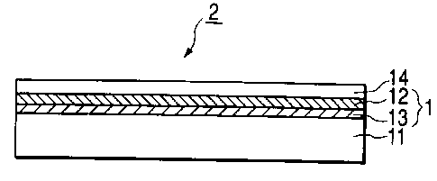
invention. As shown in Fig. lA, there is prepared a
first substrate 2 having a porous region 1 with at
CA 02233llS l998-03-2S
- 22 -
least two layers 12 and 13 different in porosity from
each other and a non-porous layer 14 formed on the
porous region 1. Reference numeral 11 denotes a base
member.
Then, as shown in Fig. lB, a surface of the non-
porous layer 14 on the first substrate 2 iS bonded to a
surface of a second substrate 3. Reference numeral 15
denotes a non-porous insulating layer, and 16 is a base
member.
Thereafter, as shown in Fig. lC, the first
substrate 2 and the second substrate 3 are separated
from each other in such a manner that the non-porous
layer 14 is transferred to the second substrate 3.
Subsequently, as shown in Fig. lD, a residual
portion 12' of the porous layer 12 remaining on a
separation surface of the second substrate 3 is removed
or made non-porous to smooth the separation surface.
In particular, as shown in Fig. lA, in the case
where the first substrate 2 iS prepared, the first
porous layer 12 adjacent to the non-porous layer 14 in
the porous region may preferably be made to have a
thickness of 1 ~um or less, more preferably to 0.5 ~m or
less. The porosity (PS2) of the second porous layer 13
adjacent to the first porous layer 12 is made higher
than the porosity (PS1) of the first porous layer 12.
When the first porous layer 12 having a lower
porosity (PS1) interposed between the non-porous layer
CA 02233ll~ l998-03-2
-- 23 --
14 and the second porous layer 13 having a higher
porosity ( PS2 ) iS thinned to 1 ~m or less, the two
substrates are separated from each other in the
vicinity of an interface between the first porous layer
and the second porous layer substantially in parallel
with the surface of the non-porous layer 14.
The residual portion 12 ' of the first porous layer
remaining on the surface of the non-porous layer which
has been transferred to the second substarate is of a
lower porosity (PS1), and made thin and substantially
uniform in thickness over the entire separation
surface. The residual portion 12' of the first porous
layer is changed into a non-porous structure by
subjecting the residual portion 12' to heat treatment
in a non-oxidizing atmosphere and integrated with the
non-porous 14 layer which is an underlying layer to be
made smooth its surface. As seen in above, upon the
removal of residual portion 12', it takes extremely
short time for etching without conducting selective
etching or polishing.
The porosity PS1 of the first porous layer
according to the present invention may preferably be
selected from a range that does not exceed 40%.
Specifically, the porosity PS1 may be 1 to 40%.
More preferably, its upper limit may be selected
from a range that does not exceed 25~. In particular,
the upper limit thereof may be 1 to 25~.
CA 0223311S 1998-03-2S
- 24 -
The porosity PS2 of the second porous layer
according to the present invention may satisfy the
relation of PS2 > PSl. It may be preferably made
higher than 25%, and more preferably made higher than
40%. In particular, the porosity PS2 may be set to 25
to 90%, and more preferably 40 to 90%.
The thickness of the second porous layer may be
selected from a range of from 10 nm to 1 ,um. More
preferably, the thickness of the second porous layer
may be made larger than that of the first porous layer.
The first substrate used in the present invention
may include, for example, one in which after the
surface of the semiconductor base member 11 is made
porous, a non-porous layer is formed on the porous
region, one in which a porous layer and a non-porous
layer are formed on the base member 11, and one in
which after the surface of the base member is made
porous, a surface layer of the region made porous is
returned to a non-porous structure.
The non-porous layer used in the present invention
includes a semiconductor formed by at least either
epitaxial growth on the porous region or treatment for
changing the porous region to a non-porous structure.
In particular, the non-porous layer is made of
semiconductor such as non-porous single crystal Si,
GaAs or InP and shaped in a plate or a disc. Also, it
is not essential that such a thin film is formed over
CA 0223311~ 1998-03-2
-- 25 --
the entire surface, but the thin film may be partially
etched by a patterning process.
An insulating layer such as an oxide film may be
formed on the surface side of the non-porous layer.
For example, the porous region can be formed by
anodizing Si substrate in an HF solution. The porous
layer is structured like sponge where holes or pores of
about 10~1 to 10 nm in diameter are arranged at
intervals of about 10~1 to 10 nm. The density of the
porous layer can be changed in a range of 2.1 to 0.6
g/cm3 by changing the concentration of HF solution in a
range of 50 to 20%, changing alcohol addition ratio or
changing a current density, in comparison with the
density of single crystal Si, 2.33 g/cm3. Also, if the
specific resistance and electric conduction type of a
portion which is made porous are modulated in advance,
the porosity can be changed on the basis of such
modulation. In case of the p type, under the same
anodization conditions, a non-degenerate substrate (P~)
is smaller in hole diameter than a degenerate substrate
(P~), but its hole density is increased by about 1
figure with the result that the porosity is high. In
other words, the porosity can be controlled by changing
these conditions. In this way, in addition that the
density of the porous Si can be reduced to the half or
less of that of single crystal Si, the single
crystallinity is maintained so that a single crystal
CA 0223311S 1998-03-2S
- 26 -
layer can be made to epitaxially grow on an upper
portion of the porous layer. However, at a temperature
of l,000~C or higher, pores inside of the porous layer
are rearranged, to thereby lose accelerating etching
characteristics. Therefore, it is presumed that a low-
temperature growth such as a molecular beam epitaxial
growth, plasma CVD, reduced pressure CVD method, photo-
assisted CVD, a bias sputtering method, a liquid-phase
growth method or the like is proper for the epitaxial
growth of an Si layer on the porous layer. However,
high-temperature growth is enabled provided that a
protective film is formed in advance on each of the
side wall surfaces of the pores formed in the porous
layer through a technique such as oxidation.
Then, the porous layer is progressively increased
in surface area more than volume because a large number
of micro-cavities are formed inside thereof. In
addition, semiconductor material merely exists as a
very-thin wall. For that reason, the chemical etching
rate is considerably accelerated in cooperation with
the suction of an etchant due to capillary action in
comparison with the etching rate of a normal single
crystal layer.
The mechanical strength of the porous region
depends on porosity, but it is presumed that it is
weaker than that of a bulk. Also, the mechanical
strength becomes weakened more as the porosity is
CA 0223311~ 1998-03-2
-- 27 --
higher. In other words, if compression, pulling force
or shearing force is exerted on the bonded wafer, the
porous layer gets first broken. Also, as the porosity
is increased, the porous layer can be destroyed by a
weaker force.
The structure of the porous region according to
the present invention has at least two layers different
in porosity where two layers from the surface side
consist of a thin layer low in porosity and a layer
high in porosity in the stated order. With the
arrangement where a porous layer low in porosity is
disposed on the surface, the crystallinity and surface
roughness of the non-porous layer formed on the porous
region, in particular, the epitaxial layer are
remarkably improved. The crystallinity greatly
influences the characteristic of the electronic device
formed on the semiconductor substrate as well as the
yield. For example, in the case where the crystal
defects in the epitaxial layer on the porous layer of
50~ in porosity is 1 x 10⁵/cm2, the crystal defects in
the epitaxial layer on the porous layer of 20% in
porosity is 5 x 10³/cm2 which is different by one and
half figures under the same growing condition. Also,
if the surface roughness is represented by mean square
roughness Rrms in the measurement of an area of 50 ~m
square by an atomic force microscopy, the respective
roughnesses are 1.2 nm and 0.3 nm, thus being largely
CA 0223311~ 1998-03-2
-- 28 --
different. Incidentally, a large surface roughness is
disadvantageous to the bonding process.
The first porous layer wiht a low porosity at the
surface is nearly 1 ,um or less in thickness, but if it
is more preferably 0.5 ~m or less, the residual layer
can be made non-porous by the surface smoothing process
after the separating step, and the surface can be
smoothed. Under this condition, if the porosity of the
first porous layer with a low porosity is 40% or less,
and more preferably 25% or less, both of the crystal
quality and the surface roughness of the epitaxial
layer can be satisfied.
The second porous layer with a high porosity
directly under the first porous layer with a low
porosity can be fabricated by controlling the above-
described various conditions of anodization, and the
thickness of the second porous layer is safisfactorily
10 nm or more, and it is desirable that the thickness
is 1 ~m or less, more preferably 0.5 ,um or less from
20 the viewpoint of restricting a separation position. No
problem particularly arises even if a third porous
layer is formed directly under the second porous layer,
and if the porosity of the third porous layer directly
under the second porous, high porosity layer is made
lower than that of the second porous layer, the
separation position is more stabilized, to thereby
improve the surface roughness after the surface
CA 02233ll~ l998-03-2
-- 29 --
smoothing treatment is conducted subsequent to the
separating step.
Also, the second porous layer with a high porosity
can be formed by using the porous structure producing
process and ion implantation together.
For example, there has been reported that when
ions of helium or hydrogen are implanted into bulk Si
and a heat treatment is then conducted on the bulk Si,
micro-cavities several to several tens nm in diameter
are formed with the density of 1016~17/cm3 or less in a
region as implanted (For example, A.Van Veen,
C.C.Griffioen, and J.H. Evans, Mat, Res. Soc. Symp.
Poroc. 107( 1988, Material Res. Soc. Pittsburgh,
Pennsylvania) p.449).
In recent years, it has been also researched that
the micro-cavity group is employed as the gettering
site of metal impurities.
V. Raineri and S.U. Campisano have implanted
helium ions into bulk Si, and conducted a heat
20 treatment to form a cavity group, and thereafter formed
a groove in a substrate so that the side surface of the
cavity group is exposed, and conducted an oxidation
treatment. As a result, the cavity group was
selectively oxydized to form a buried Si oxide film.
In other words, they have reported that the SOI
structure can be formed (V. Raineri, and S.U.
Canpisano, Appl. Phys. Lett. 66 (1995) p.3654).
CA 0223311~ 1998-03-2
-- 30 --
However, in their methods, the thicknesses of the
surface Si layer and the burried Si oxide layer are set
within the limits that both of the formation of the
cavity group and the relief of a stress developed by
the expansion of a volumn at the time of oxidation are
satisfied, and also the formation of a groove is
required for selective oxidation. As a result, the SOI
structure could not be formed over the entire
substrate. The formation of the cavity group has been
reported as a link of the research relating to the
inflation of those cavity groups and the separation
phenomenon as well as a first furnace wall of a nuclear
fusion reactor as a phonomenon accompanied with the
implantation of light elements into a metal.
There has been well known that bubbles occur in
the ion implanted layer as described above, and the ion
implanted layer is structured as if porous structure is
formed inside of the ion implanted layer. Therefore,
that layer is mechanically weak and enables
acceleration oxidation and acceleration etching as in
the porous quality of anodization.
The ion implantation elements are not limited to
hyrogen or rare gas, if an implantation damage layer, a
high-concentration layer (strain layer) of implanted
elements or a bubble layer is formed in the vicinity of
the interface.
Provided that ion implantation is conducted in
CA 0223311~ 1998-03-2~
such a manner that a projection range is contained in
the porous layer formed by anodization, bubbles are
formed in pore walls of the porous material in the
vicinity of the projection range, to thereby enhance
the porosity. The ion implantation may be made before
or after the formation of the porous layer by
anodization. Further, the ion implantation may be made
even after the non-porous layer structure is formed.
In the epitaxial growth process on the porous
layer, as its first step, baking (heat treatment) in H2
for embedding the surface pores of the porous Si is
greatly effective in making the quality of the
epitaxial layer high (N. Sato, et al., J. Electrochem.
Soc., Vol. 142, No. 9, 3116 (1995)). The constituent
atoms of the outermost surface porous layer are
consumed for embedding the holes during the H2 baking
process. Therefore, if the outermost surface before
being H2-baked is a thin layer low in porosity, the
sealing of the pores during the hydrogen baking process
is promoted. If the thin layer low in porosity is made
thin to about 1 ~m or less, more preferably 0.5 ,um or
less, a porous layer having a high porosity can be
disposed downward in the vicinity of the epitaxial
layer which has been subjected to epitaxial growth, so
that the separation can occur in the porous region
close to the epitaxial layer. Also, the thickness of
the thin layer having a low porosity remaining after
CA 02233115 1998-03-25
- 32 -
separation can be set to a value lower than 1 ~m,
sometimes lower than 0.5 ~m so as to be smoothed in the
subsequent smoothing process. Also, provided that the
base member where a porous region is formed is immersed
in the HF solution prior to H2 baking to remove the
oxide film on the porous side wall of the pores in the
vicinity of the surface of the porous layer, the oxide
film is removed by HF, and a portion of the exposed
surface layer which has not been made non-porous
developes coagulation of pores during the heat
treatment including the H2 baking process, and has no
oxide film on the side wall of the pores, and further
becomes weakened in mechanical strength, to thereby
form a layer at which separation is easily made.
After the anodization, when the porous layer is
subjected to a high-temperature process such as
epitaxial growth, surface oxidation or bonding heat
treatment without being oxidized at a low temperature,
the porous layer is structurally changed such that the
fine pores at the time of anodization is agglomerated
and enlarged. Employing this phenomenon, separation
can be promoted in the vicinity of the interface
between of the epitaxial and porous layer due to the
enlargement of the pores directly under the epitaxial
layer and the strain between the porous Si and the
epitaxial Si.
In the present invention, subsequent to the
CA 0223311~ 1998-03-2~
separation of the bonded wafer at the second porous
layer high in porosity, the residual portion low in
porosity l- ~;ning on the surface of the transferred
non-porous layer is subjected to a smoothing process.
A heat treatment under a non-oxidizing atmosphere
or a heat treatment in a vacuum is proper for the
smoothing process, but the smoothing process is not
limited by those treatments. In the heat treatment,
hydrogen, inert gas such as He, Ne, N, Ar, Kr, Xe or
the like, or an atmosphere where those gases are mixed
is particularly desirable as the non-oxidizing
atmosphere. In the heat treatment in a vacuum, the
vacuum is desirable 10-7 Torr or below. In any cases,
the residual oxygen and water remaining in the
atmosphere as impurities oxidize the surface to form a
protective film. Since the protective fim impedes the
smoothing of the surface, residual oxygen and water
need to be lowered. It is desirable that the
atmosphere is set to -92~C or below.
In case of such an atmosphere, the surface
roughness is smoothed by migration of the surface atoms
which minimizes the surface energy. In particular, if
hydrogen is contained in the atmosphere, the formation
of the protective film is restrained by its reducing
action to promote surface smoothing. As a result of
studying the relation between the surface smoothing
effect and the thickness of the residual porous layer,
CA 0223311~ 1998-03-2
-- 34 --
the present inventors have found that if the thickness
of the porous layer is about 1 ~um or less, more
preferably 0.5 ,um or less, the surface is smoothed by a
heat treatment, and cavities resulting from the
residual pores can be prevented from being produced in
the layer which has been smoothed, that is, the layer
can be made non-porous. In the case where the residual
porous layer is thick, the residual pores are liable to
remain in the interior of the layer. In the flattening
due to the heat treatment, since the surface smoothing
is progressed by migration of the surface atmos, the
etching quantity is restrained to be extremely low. In
particular, in the case where the residual oxygen and
water in the atmosphere are restrained to be low, the
etching amount can be set almost to 0.
As has been reported up to now, because no long
selective etching process needs to be used, in addition
to the effect of the reduction or deletion of the
process, there hardly occurs a problem such as the
deterioration of the uniformity of the layer thickness
due to excessive etching of the non-porous layer which
occurs when the selective ratio of etching is not
sufficient. Therefore, the uniformity of the epitaxial
Si layer as the non-porous layer is not deteriorated at
all.
According to the present invention, the epitaxial
Si film formed on the single crystal porous layer as
CA 02233ll~ l998-03-2
-- 35 --
the non-porous layer can be separated and transferred
to another substrate without conducting selective
etching. In particular, because a defect inherent to
bulk Si is not propagated to the epitaxial Si film, the
yield of the device can be improved. Even at the
present, the epitaxial wafer is used for high-
performance LSI such as a CPU. It is said that an
increase in the diameter of wafer is propagated in the
future, making it difficult to manufacture high-quality
crystal through a pull method, and it is presumed that
keeping of the quality of wafer is difficult.
Therefore, the necessity of the epitaxial wafer is
increased more and more. It is needless to say that
the necessity of the epitaxial film is increased in the
15 SOI base member by which the bulk wafer is replaced.
Also, because the electric conductive type and the
impurity concentration of the non-porous layer can be
set arbitrarily by controlling the electric conductive
type and the impurity concentration at the time of
epitxial growth, various SOI substrates different in
electric conductive type or impurity concentration can
be manufactured from the same first substrate.
Furthermore, if the epitaxial film having a multi-
layer structure different in the electric conductive
type and impurity concentration is formed, in
particular, an SOI substrate having a high-
concentration burried layer can be manufactured as a
CA 0223311~ 1998-03-2
-- 36 --
multi-layer SOI substrate from the original.
The above wide and various operations are
disenabled by a method as disclosed in Japanese Patent
Application Laid-Open No. 5-211128 in which the
outermost surface layer of bulk wafer is peeled off by
ion implantation and then transferred to another
substrate.
Also, in the case where both of the porous region
and a underlying layer portion of the non-porous layer
which is in contact with the porous region are formed
of epitaxially grown layers, the first substrate can be
reused semi-permanently without reduction in the
thickness of the substrate even if it is used many
times. Hence, in addition to the enhancement of the
quality, the above structure has great advantages from
the viewpoints of the resource saving and the costs,
particularly in the large-diameter wafer.
Also, in the compound semiconductor single
crystal, it was difficult and expensive to obtain a
wafer large in diameter and excellent in crystallinity.
According to the present method, using hetero-epitaxial
growth on the porous Si region, a compound
semiconductor single crystal film excellent in
crystallinity can be formed on a large-area substrate.
On the other hand, in the present invention, the
surface layer of the substrate made porous can be
transformed into a non-porous single crystal layer by a
CA 0223311~ 1998-03-2~
heat treatment at a temperature of the melting point or
below. In this case, the non-porous single crystal
layer excellent in crystallinity can be formed on the
surface of the substrate made porous without using a
semiconductor source gas such as silane. Also, after
the surface of the non-porous single crystal layer as
formed is oxidized and then bonded to another
substrate, the non-porous single crystal layer is
bonded to another substrate whose surface is oxidized,
or the surfaces of both the substrates are oxidized and
bonded to each other, those substrates are separated at
the high porosity layer, and then the residual portion
low in porosity is smoothed. As a result, there can be
formed a single crystal layer having an excellent
single crystal structure on the oxide layer, uniformly
flat over the large area and remarkably reduced in
defects.
Further, in the method of manufacturing the
semiconductor substrate according to the present
invention, after the residual porous layer is removed,
or remains as it is if the removal is unnecessary, it
is subjected to surface flattenning processing if the
surface flatness is insufficient, whereby the first Si
substrate separated by the above method can be reused
as a first base member, as a subsequent second base
member or as a base member used for another purpose.
The surface flattening processing may be conducted by a
CA 0223311~ 1998-03-2
-- 38 --
polishing or etching method, etc., used in a normal
semiconductor process, or may be conducted by a heat
treatment under a non-oxidizing atmosphere. Hydrogen,
inert gas or an atmosphere where those gases are mixed
is particularly desirable as the non-oxidizing
atmosphere. Alternatively, it may be a heat treatment
in vacuum. The heat treatment can locally flatten it
to the degree that the atom step appears locally by
selecting the conditions.
Also, in the case where the first substrate after
the non-porous layer is transferred is again repeatedly
used as a first base member, the first base member can
be reused many times until it cannot be forcedly used.
Because the first substrate is held to the
original without being made porous other than the
surface layer, both the surfaces of the first substrate
are regarded as main surfaces, and base members are
bonded to the respective surfaces, thereby being
capable of manufacturing a two-sheet bonded SOI
substrate from one first substrate at the same time.
Thus, the process can be shortened to improve the
producibility. The separated first substrate can be
reused.
The substrate thus obtained can be substituted for
expensive SOS or SIMOX when the large-scaled integrated
ciruit of the SOI structure is manufactured.
As the second substrate, there are, for example,
CA 02233ll~ l998-03-2
-- 39 --
an Si base member and an Si oxide film formed on the Si
base member. Or it may be a light transmissive
insulating base member such as quartz, fused quartz,
silica glass, glass or sapphire, or a metal base
member. Thus, it may not be limited particially.
Referring to Figs. 2A to 2F, an embodiment of the
present invention will be described.
As shown in Fig. 2A, there is prepared a first Si
single crystal base member 11, and a porous region
consisting of at least two layers having a first porous
layer 12 of low porosity and a second porous layer 13
of high porosity on the main surface from the surface
side. The layer 13 consists of at least one layer.
The porous Si can be formed by conducting anodization
on the Si base member in the HF solution. The
thickness of the low porosity thin layer is described
above. On the other hand, the high porosity layer of
the second porous layer is higher in porosity than the
low porosity thin layer. In the case where a third
porous layer is further formed lower than the high
porosity layer, the second porous layer is desirably
higher in porosity than the third porous layer. In
other words, it is desirable that the porosity of the
second porous layer is the largest in the porous
region. Also, the thickness of the second porous layer
is described above.
As shown in Fig. 2B, at least one non-porous layer
CA 0223311~ 1998-03-2
-- 40 --
14 iS formed on the porous regions 12 and 13. The non-
porous layer 14 iS formed of the above-described
materials, including particularly single crystal Si,
polycrystal Si, amorphous Si, a metal film, a compound
semiconductor thin film, a super-conductive thin film
or so on. A device structure such as MOSFET may be
formed on the non-porous layer. If it is of the multi-
layer structure, it may be an SOI having a burried
layer. Further, it is better to form an insulating
film 15 such as SiO2 on the outermost layer because the
interfacial level of the bonded surface can be isolated
from an active layer.
As shown in Fig. 2C, the surface of a second base
member 16 and the surface of the first substrate are
made to adhere to each other at a room temperature.
Fig. 2C shows a state where the second base member
and the first substrate are bonded to each other
through the insulating layer 15. In the case where the
non-porous layer 14 iS not Si or the second base member
is not Si, no insulating layer 15 may be provided.
In bonding the substrates, an insulating thin
plate may be interposed therebetween so that they may
be bonded in a three-sheet superimposed manner.
As shown in Fig. 2D, the substrates are separated
at the outermost thin film in the second porous layer
13 on the first porous layer 12 side. The separating
method may be a method of applying an external pressure
CA 0223311~ 1998-03-2~
due to pressure, tensile force, shearing force or a
wedge, a method of applying a supersonic wave, a method
of applying a heat, a method of applying an inner
pressure to the interior of the porous region by
inflating the porous Si from the periphery by
oxidation, a method of heating in a pulse-like manner
to apply a heat stress, a method of softening or the
like. But, it is not limited by or to those methods.
Subsequently, the smoothing processing is
conducted on the surface of the second substrate which
accompanies the non-porous quality producing action on
the residual portion of the first porous layer 14. The
smoothing process is described above.
As a result of the above, the semiconductor
substrate shown in Fig. 2E is obtained. The non-porous
layer 14, for example, single crystal Si thin film is
made thin flatly and uniformly on the second base
member 16 and formed in a large area over the entire
wafer. If the second substrate and the first substrate
are bonded to each other through the insulating layer
15, there is formed a semiconductor substrate suitable
for the manufacture of the electronic device
insulation-isolated.
The first Si single crystal base member 11 is
reused as a first base member 11 or as a second base
member 16 after the residual portion of the second
porous layer is removed if it is unnecessary and the
CA 0223311~ 1998-03-2
- 42 -
surface is smoothed in the case where the surface is
rough to the degree that the surface smoothness is not
acceptable as shown in Fig. 2F, and the process shown
in Figs. 2A to 2F is again repeated to manufacture
another semiconductor substrate.
The semiconductor manufacturing process shown in
Figs. lA to lD or 2A to 2F is conducted on both
surfaces of the first base member using two second base
members so that two semiconductor substrates can be
manufactured at the same time. This method is shown in
Figs. 3A to 3F.
The first base member 11 can be reused as a first
base member 11 or as one of two second base members 16
after the residual porous layers 13 on both the
surfaces are removed if they are unnecessary and the
surface is smoothed in the case where the surface is
rough to the degree that the surface smoothness is not
acceptable.
The two base members 16 may not be identical in
size and material.
The two non-porous layers 14 may not be identical
in size and material.
No insulating material 15 may be provided.
Because the conventional bonding substrate
manufacturing method is made using a method of
sequentially removing the first Si base member from one
surface thereof by polishing or etching, it is
CA 0223311~ 1998-03-2
-- 43 --
impossible that both the surfaces of the first Si base
member is effectively utilized and bonded to another
base member. However, according to the above
embodiment, because the first Si substrate is
maintained as it is except for its surface layer, both
the surfaces of the first Si substrate can be used as
main surfaces, and a base member can be bonded to each
the surface, so that two bonded substrates can be
manufactured from the single first Si base member at
the same time. As a result, the process can be reduced
and the productivity can be improved. It is needless
to say that the separated first Si base member can be
reused.
For example, in case of a silicon base member, the
surface layer of the silicon base member is made porous
and transformed into a non-porous silicon single
crystal layer by a heat treatment using a temperature
of the melting point or less after the Si base member
is made porous. As a result, a silicon single crystal
layer excellent in crystallinity can be formed on the
surface of the silicon base member made porous without
using a silicon-containing source gas such as silane.
Figs. 4A to 4C schematically show the appearance
of the porous region in a step of forming the first
porous layer and the second porous layer, a step of
forming the non-porous layer and a separating step
according to the present invention.
CA 0223311~ 1998-03-2
-- 44 --
Fig. 4A schematically shows an appearance where a
low porosity layer 12a low in porosity and having pores
Pl and a second porous layer 13 high in porosity and
having holes P2 with a larger diameter than the pores
P1 are formed on the surface of the base member 11.
Fig. 4B schematically shows an appearance where a
portion of the low porosity layer 12a on the surface
side is made non-porous by conducting a heat treatment
to form a non-porous layer 14 as a process of forming
the non-porous layer. In other words, a laminated body
consisting of the second porous layer 13, the first
porous layer 12 and the non-porous layer 14 are formed
on the surface of the base member 11.
Fig. 4C schematically shows an appearance where
the substrates have been separated, that is, an
appearance where an interface portion of the second
porous layer on the interface if side between the first
porous layer 12 and the second porous layer 13 is
partially destroyed and separated.
Figs. 4A to 4C schematically show the respective
appearances for facilitation of understanding the
present invention. However, the form of the pores in
the porous layer and the configuration of the separated
surface are usually more complicated.
Also, the thickness of the non-porous layer 14 may
be increased by conducting epitaxial growth, etc.,
after the non-porous quality producing process
CA 0223311~ 1998-03-2
-- 45 --
(Fig. 4B).
(Example 1)
A surface layer of a first single crystal Si
substrate was anodized in an HF solution.
The anodization conditions are stated below.
Current density: 7 (mA-cm~2)
Anodization solution: HF:H20:C2HsOH = 1:1:1
Period of time: t (min)
Thickness of porous Si: x (,um)
Further,
Current density: 50 ( mA-cm~2)
Anodization solution: HF:H20:C2H50H = 1:1:1
Period of time: 10 (sec)
Thickness of porous Si: 0.2 (,um)
The first anodization period t was changed to 0,
0.2, 0.5, 1.0 and 1.5 min, respectively such that a
thickness of a first porous layer having a low porosity
becomes 0, 0. 2, 0 . 5, 1 . O and 1.5 ~m.
Through the anodization where the current density
was set to 50 mA-cm~2, the porosity of a second porous
Si layer becomes large, to thereby form a thin film
having a high porosity which is structurally fragile.
After being inserted into an epitaxy apparatus,
the wafer was disposed in hydrogen atmosphere and baked
at 1,060~C. When the sample was taken out in this
state and observed through a scanning electron
microscope, it was recognized that the surface pores of
CA 0223311~ 1998-03-2
-- 46 --
the porous Si were sealed. As a result, the outermost
surface layer of the thin film having a low porosity
was consumed for burying the holes and came to a non-
porous state. In particular, the low porosity layer
was formed in a predetermined thickness of 1.0 ~um or
less, and thereafter the surface layer was made non-
porous, and the remaining low porosity layer became 0.5
,um or less in thickness. Sequentially, single crystal
Si was allowed to epitaxially grow in a thickness of
0.3 ~um on the porous Si through a CVD (Chemical Vapor
Deposition) method. The growth conditions are stated
below.
Source gas: SiH2C12/H2
Gas flow rate: 0.2/180 l/min
Gas pressure: 760 Torr
Temperature: 1060~C
Growth rate: 0.15 ,um/min
Furthermore, an SiO2 layer of 200 nm thickness was
formed on the surface of the epitaxial Si layer through
thermal oxidation.
After the surface of the SiO2 layer was
superimposed on a surface of another Si substrate
(second substrate) and brought into contact with the
latter, the substrate was annealed at 1180~C for 5
minutes, with the result that the bonding became firm.
As a result of separating the bonded wafers, they
were divided in the vicinity of an interface in the
CA 02233ll~ l998-03-2
-- 47 --
high porosity layer between the high porosity layer and
the low porosity layer. Any methods may be used for
separation. Subsequently, the substrate was located in
a normal-pressure hydrogen atmosphere and subjected to
a heat treatment at 1100~C for 4 hours. As a result,
the thin layer having a low porosity remaining on the
second substrate was completely made non-porous. As a
result of observing the section of the thin layer
through an electron microscope, any remaining voids
could not be confirmed. As a result of observing a
surface roughness through an atomic force microscope,
it could be recognized that the root mean square
roughness in a region of 50 ,um square was about 0.5,
0.2, 0.2, 0.4 and 1.5 nm when the thickness of the
porosity layer was 0, 0.2, 0.5, 1.0 and 1.5 ,um, and a
surface roughness of the thin layer having a low
porosity which is 1.0 ~m or less in thickness was
equivalent to that of the Si wafer normally on the
market. Likewise, as a result of measuring the crystal
defect density, the lamination defect density was about
1 x 10⁵, 6 x 10³, 5 x 10³, 5 x 10³, and 5 x 10³/cm2 when
a thickness of the low porosity layer was 0, 0.2, 0.5,
1.0 and 1.5 ~m, and crystal defect density was
remarkably reduced by introduction of the thin layer
with a low porosity.
In the above way, the single crystal Si layer with
a low defect density could be formed on the Si oxide
CA 0223311S 1998-03-2S
- 48 -
film. When the thickness of the single crystal Si
layer as formed was measured over the entire surface at
100 points, the uniformity of the thickness was 211+4
nm, 412+9 nm, 690+14 nm, 1201+24 nm and 1707+34 nm,
respectively. Since the single crystal Si layer also
includes a portion where the low porosity layer is made
non-porous, the thickness thereof is different.
The roughness remaining on the first Si substrate
side was subjected to surface treatment such as
hydrogen annealing or surface polishing as the surface
smoothing process, the substrate could be used again as
a first substrate or as a second substrate. In this
situation, when the porous Si remains in a relatively
large amount, selective etching may be conducted using
a mixed solution consisting of 49~ hydrofluoric acid
and 30~ hydrogen peroxide solution while stirring, and
thereafter the substrate may be subjected to surface
treatment such as hydrogen annealing or surface
polishing, so that the substrate may be again used as a
first substrate or as a second substrate.
(Example 2)
A surface layer of a first single crystal Si wafer
was anodized in an HF solution.
The anodization conditions are stated below.
Current density: 7 (mA cm~2)
Anodization solution: HF:H20:C2HsOH = 1:1:1
Period of time: 0.1 (min)
CA 0223311~ 1998-03-2~
_ ~9 _
Thickness of first porous Si layer: 0.1 (~m)
Further,
Current density: 50 (mA-cm~2)
Anodization solution: HF:H20:C2HsOH = 1:1:1
Period of time: 5 (sec)
Thickness of second porous Si layer: 0.1 (,um)
Still further, a third layer may be manufactured.
The conditions are, for example, stated below.
Current density: 7 (mA-cm~2)
Anodization solution: HF:H20:C2HsOH = 1:1:1
Period of time: 1 (min)
Thickness of third porous Si layer: 1 (,um)
Through the anodization, the porosity of the
porous Si layer becomes the largest in the porous
region where the current density was set to 50 (mA-cm),
whereby a high porosity layer which is structurally
fragile was formed under the thin layer having a low
porosity.
Thè wafer was oxidized at 400~C for one hour in an
oxygen atmosphere. Through this oxidation, the inner
wall of each the hole in the porous Si was covered with
a thermal oxide film. The wafer was immersed in the HF
aqueous solution of 1~ for about 30 seconds, to thereby
remove the very-thin thermal oxide films formed on the
surface of the porous Si and the inner walls of the
holes in the vicinity of the surface. After being
inserted into a super-high vacuum device, the wafer was
CA 0223311~ 1998-03-2
-- 50 --
baked at 1000~C under 1 x 10⁻⁹ Torr for 5 minutes. The
sample was taken out in the above state and observed
through a scanning electron microscope. It has been
recognized that the surface holes of the porous Si were
sealed. As a result, the outermost surface layer of
the thin layer having a low porosity was consumed for
burying the holes and came to a non-porous state.
Sequentially, the substrate was located in an epitaxial
growth device, and the single crystal Si was allowed to
epitaxially grow in a thickness of 1 ,um on the porous
Si through a CVD method. The growth conditions are
stated below.
Source gas: SiH2C12/H2
Gas flow rate: 0.4/180 l/min
Gas pressure: 80 Torr
Temperature: 900~C
Growth rate: 0.15 ~m/min
Furthermore, an SiO2 layer of 200 nm thickness was
formed on the surface of the epitaxial Si layer through
thermal oxidation.
After the surface of the SiO2 layer was
superimposed on a surface of another Si substrate
tsecond substrate) and brought in contact with the
latter, the substrate was annealed at 1100~C for 10
minutes, with the result that the bonding became firm.
As a result of separating the bonded wafers, in
the case where anodization current density of a third
CA 02233ll~ l998-03-2
-- 51 --
layer was set to 7 mA/cm2, they were divided in the
vicinity of an interface between the first porous layer
and the second porous layer in the high porosity layer
of the second layer. In other words, when the porosity
of the second layer was set to the largest porosity in
the porous layer structure, separation was readily
made. Subsequently, the second substrate was located
in a hydrogen atmosphere under a pressure of 50 Torr,
and subjected to a heat treatment at 1100~C for 2
hours. As a result, the thin layer having a low
porosity remaining on the surface of the epitaxial Si
layer transferred onto the second substrate was
completely made non-porous. As a result of observing
the section of the thin layer through an electron
microscope, no residual oavities, etc., could be
recognized. As a result of evaluating the surface
roughness through an atomsic force microscope, the mean
square roughness in a region of 50 ~m square was about
0.3 nm, and the surface roughness was equivalent to
that of the Si wafer normally on the market. Likewise,
as a result of measuring the crystal defect density,
the lamination defect density was 5 x 10³/cm2, and
crystal defect density was remarkably reduced by
introduction of the thin layer having a low porosity.
As a result of the above, the single crystal Si
layer with a low defect density could be formed on the
Si oxide film of the second substrate. As a result of
CA 0223311~ 1998-03-2~
measuring a thickness of the single crystal Si layer as
formed over the entire surface at lO0 points,
uniformity of the thickness was 1011+22 nm,
respectively.
Even if the oxide film is formed not on the
surface of the epitaxial layer but on the surface of
the second substrate, or on both of those surfaces, the
same effects could be obtained.
The porous Si remaining on the surface of the
second substrate was selectively etched using a mixted
solution consisting of 49~ hydrofluoric acid and 30%
hydrogen peroxide solution while stirring. Thereafter,
the substrate was subjected to surface treatment of
hydrogen annealing, so that the substrate could be used
as a first substrate again or as a second substrate.
(Example 3)
A surface layer of a first single crystal Si
substrate was anodized in an HF solution.
The anodization conditions are stated below.
Current density: 7 (mA cm~2)
Anodization solution: HF:H20:C2H50H = 1:1:1
Period of time: 3 (min)
Thickness of porous Si: 3 (,um)
The substrate was oxidized under an oxygen
atmosphere at 400~C for 1 hour. Through the oxidation,
the inner walls of the respective holes in the porous
Si were covered with thermal oxide films. Ion
CA 0223311~ 1998-03-2~
implantation was made in such a manner that a
projection range from the wafer surface came in the
porous Si and in the vicinity of a portion apart from
the surface by 0.3 ,um. The ion implantation elements
are not particularly limited, but any elements can be
applied if an implantation damage layer, a high-
concentration layer (strain layer) of implanted
elements or a bubble layer is formed in the vicinity of
the interface.
The single crystal Si was allowed to epitaxially
grow in a thickness of 0.15 ,um on the porous Si through
a CVD method. The growth conditions are stated below.
Source gas: SiH2C12/H2
Gas flow rate: 0.5/180 l/min
Gas pressure: 80 Torr
Temperature: 900~C
Growth rate: 0.15 ,um/min
Furthermore, an SiO2 layer of 100 nm thickness was
formed on the surface of the epitaxial Si layer through
thermal oxidation.
After the surface of the SiO2 layer was
superimposed on a surface of another Si substrate
(second substrate) and brought in contact with the
latter, the substrate was annealed, with the result
that the bonding became firm. The annealing is
conducted under the conditions where an implantation
damage layer, a high-concentration layer (strain layer)
CA 02233ll~ l998-03-2
-- 54 --
of implanted elements or a bubble layer is not
diffused. As a result of observing the section of the
thin layer through an electron microscope, it could be
recognized that the porosity of the porous layer at a
position where ions were implanted increased. That is,
a high porosity layer which will form a separation
layer later was formed by ion implantation.
As a result of separating the bonded wafers, they
were divided at the high porosity layer which was
formed by ion implantation.
Sequentially, the second substrate was located in
an atmosphere where H2 was diluted with Ar and subjected
to a heat treatment at 1200~C for 2 hours. As a
result, the thin layer having a low porosity remaining
15 on the surface of the single crystal Si layer
transferred onto the second substrate was completely
made non-porous. As a result of observing the section
of the thin layer through an electron microscope, no
residual cavities, etc., could be recognized. As a
result of evaluating the surface roughness through an
atomic force microscope, the mean square roughness in a
region of 50 ~m square was about 0.3 nm, and the
surface roughness was equivalent to that of the Si
wafer normally on the market. Likewise, as a result of
measuring the crystal defect density, the lamination
defect density was 6 x 10³/cm2, and crystal defect
density was remarkably reduced by introduction of the
CA 0223311~ 1998-03-2
-- 55 --
thin layer having a low porosity.
As a result of the above, the single crystal Si
layer with low defect density could be formed on the Si
oxide film. As a result of measuring a thickness of
the single crystal Si layer as formed over the entire
surface at 100 points, the uniformity of the thickness
was 311+6.2 nm, respectively.
The porous Si l~ ~ining on the surface of the
first substrate was selectively etched using a mixted
solution consisting of 49% hydrofluoric acid and 30%
hydrogen peroxide solution while stirring. Thereafter,
the first substrate was subjected to surface treatment
of hydrogen annealing, so that the first substrate
could be again used as a first substrate or as a second
substrate.
(Example 4)
Boron was diffused on a surface of a first p~
single crystal Si substrate in advance so that a p+
layer was formed in a thickness of about 0.2 ,um.
Subsequently, the surface layer of the substrate
was anodized in an HF solution.
The anodization conditions are stated below.
Current density: 7 (mA-cm~2)
Anodization solution: HF:H20:C2HsOH = 1:1:1
Period of time: 2 (min)
As a result of observing the substrate through a
scanning electron microscope, it has been recognized
CA 0223311~ 1998-03-2
-- 56 --
that a layer having 20% porosity was formed in a
thickness of 0.2 ,um on the surface, and a porous layer
having 50~ porosity was formed in a thickness of about
0.4 ~m under that layer.
The substrate was oxidized under an oxygen
atmosphere at 400~C for 1 hour. Through the oxidation,
the inner walls of the respective holes in the porous
Si were covered with thermal oxide films. After being
inserted into an epitaxy device, the wafer was baked at
1060~C for 5 minutes, and further baked while Si source
is applied in a small amount, to thereby bury the
surface holes of the porous Si. The single crystal Si,
a p-epitaxial layer of 0.45 ~um thickness, and an n+
epitaxial layer of 1.0 ,um were allowed to epitaxially
grow on the porous Si where the surface holes were
burried through a CVD (Chemical Vapor Deposition)
method. The growth conditions are stated below.
Source gas: SiH2C12/H2
Gas flow rate: 0.5/180 l/min
Gas pressure: 80 Torr
Temperature: 900~C
Growth rate: 0.15 ~um/min
Furthermore, an SiO2 layer of 100 nm thickness was
formed on the surface of the epitaxial Si layer through
thermal oxidation.
After the surface of the SiO2 layer and a surface
of another Si substrate (second substrate) were treated
CA 02233115 1998-03-25
with ~2 plasma and washed with water, they were
superimposed one on another and brought in contact with
each other, and then annealed at 400~C for 60 minutes,
with the result that the bonding became firm.
As a result of separating the bonded wafers, they
were divided at the high porosity layer in the vicinity
of an interface of the low porosity layer.
Subsequently, the second substrate was located in
a super-high vacuum device where residual oxygen and
moisture were satisfactorily removed, and then
subjected to a heat treatment under a pressure of
1 x 10⁻⁹ Torr at 950~C for 4 hours. As a result, the
thin layer having a low porosity remaining on the
second substrate was completely made non-porous. As a
result of observing the section of the thin layer
through an electron microscope, no residual cavities,
etc., could be recognized. As a result of evaluating
the surface roughness through an atomic force
microscope, the mean square roughness of in a region of
50 ,um square was about 0.5 nm, and the surface
roughness was equivalent to that of the Si wafer
normally on the market. Likewise, as a result of
measuring the crystal defect density, the lamination
defect density was 6 x 10³/cm2, and crystal defect
density was remarkably reduced by introduction of the
thin layer having a low porosity.
As a result of the above, a single crystal Si
CA 0223311~ 1998-03-2~
layer including an n' buried layer and having the
thickness of 1.6 ,um could be formed on the Si oxide
film of the second substrate. As a result of measuring
a thickness of the single crystal Si layer as formed
over the entire surface at 100 points, uniformity of
the thickness was 1.6+0.03 ,um, respectively.
After the roughness remaining on the surface of
the first substrate side was subjected to surface
treatment with hydrogen annealing as the surface
flattening process, it could be again used as a first
substrate or as a second substrate. In the case where
the porous Si remains, selectively etching may be
conducted using a mixted solution consisting of 49~
hydrofluoric acid and 30~ hydrogen peroxide solution
while stirring. Thereafter, the first substrate may be
subjected to surface treatment such as hydrogen
annealing or surface polishing, so that the first
substrate may be again used as a first substrate or as
a second substrate.
(Example 5)
A surface layer of a first single crystal Si
substrate was anodized in an HF solution.
The anodization conditions are stated below.
Current density: 7 (mA-cm~2)
Anodization solution: HF:H20:C2H50H = 1:1:1
Period of time: 0.1 (min)
Thickness of porous Si: 0.1 (,um)
CA 0223311S 1998-03-2S
- 59 -
Then, anodization was conducted with a change of
the concentration of the solution as stated below.
Current density: 7 (mA-cm~2)
Anodization solution: HF:HzO:C2H5OH = 1:2:1
Period of time: 1 (min)
Thickness of porous Si: 0.6 (~m)
As a result of observing the substrate through a
scanning electron microscope, it has been recognized
that a high porosity layer which corresponds to a
second formation was formed in depth of about 0.1 ~m
from the surface.
The substrate was oxidized under an oxygen
atmosphere at 400~C for 1 hour. Through the oxidation,
the inner walls of the respective holes in the porous
Si were covered with thermal oxide films. The oxide
film in the vicinity of the surface of the porous Si
was removed by HF. After being inserted into an
epitaxy device, the wafer was baked in a hydrogen
atmosphere at 1040~C for 5 minutes, thus burying the
surface holes of the porous Si. A single crystal GaAs
was epitaxially grown in a thickness of 0. 5 ,um on the
porous Si where the surface holes were burried through
the MOCVD (Metal Organic Chemical Vapor Deposition)
method. The growth conditions are stated below.
Source gas: TMG/AsH3/H2
Gas pressure: 80 Torr
Temperature: 700~C
CA 0223311~ 1998-03-2
-- 60 --
After the surface of the GaAs layer and a surface
of another Si substrate (second substrate) were
superimposed one on another and brought in contact with
each other, they were annealed at 700~C for 1 hour,
with the result that the bonding became firm.
As a result of separating the bonded wafers, they
were divided at the high porosity layer in the vicinity
of an interface of the low porosity layer side.
As a result of the above, a single crystal GaAs
layer having a thickness of 0.5 ,um could be formed on
the second Si substrate. As a result of measuring a
thickness of the single crystal GaAs layer as formed
over the entire surface at 100 points, uniformity of
the thickness was 0.5+0.01 ~um, respectively.
Because the surface of the GaAs layer is rough,
and also there is a possibility that a residue the
porous Si remains, surface touch polishing is
conducted. As a result, a similar surface smoothness
to that of the GaAs wafer normally on the market was
obtained.
As a result of observing ~he section of the thin
layer through a transmission electron microscope, it
has been recognized that no new crystal defects were
introduced in the Si layer, thereby keeping excellent
crystallinity.
As the second substrate, an Si substrate whose
surface was oxidized can be used instead of the Si
CA 0223311S 1998-03-2S
substrate. Also, after a deposited SiO2 film is formed
on the surface of the Si substrate or the GaAs layer,
those substrates may be bonded to each other. In this
case, the complete substrate is used as GaAs on an
insulating substrate.
If the roughness ~ ;ns on the first substrate
side is subjected to surface treatment such as hydrogen
annealing or surface polishing to flatten the surface,
the first substrate may be again used as a first
substrate or as a second substrate. In the case where
the porous Si remains, selectively etching may be
conducted using a mixted solution consisting of 49%
hydrofluoric acid and 30% hydrogen peroxide solution
while stirring. Thereafter, the first substrate may be
subjected to surface treatment such as hydrogen
annealing or surface polishing, so that the first
substrate may be again used as a first substrate or as
a second substrate.
(Example 6)
A surface layer of a first single crystal Si
substrate was anodized in an HF solution.
The anodization conditions are stated below.
Current density: 7 (mA-cm~2)
Anodization solution: HF:HzO:CzH50H = 1:1:1
Period of time: 0.2 (min)
Thickness of porous Si layer: 0.2 (~m)
Further,
CA 02233ll~ l998-03-2
-- 62 --
Current density: 50 (mA-cm~2)
Anodization solution: HF:H20:C2H50H = 1:1:1
Period of time: 10 (sec)
Thickness of second porous Si layer: 0. 2 ( ,um)
Through the anodization, the porosity of the
porous Si layer was increased due to 50 (mA-cm~2), to
thereby form a thin layer having a high porosity which
is structurally fragile.
After being inserted into an epitaxy device, the
wafer was baked in a hydrogen atmosphere at 1060 ~ C for
5 minutes. In this state, the sample was taken out and
observed through a scanning electron microscope. It
has been recognized that the surface holes of the
porous Si were sealed. As a result, the outermost
surface of the thin layer having a low porosity was
consumed for burying the holes and came to a non-porous
state. Sequentially, a single crystal Si was
epitaxially grown in a thickness of 0.3 ~m on the
porous Si through a CVD method. The growth conditions
are stated below.
Source gas: SiH2C12/H2
Gas flow rate: 0.2/180 l/min
Gas pressure: 760 Torr
Temperature: 1060~C
Growth rate: 0.15 ,um/min
Further, an SiOz layer was formed in a thickness of
200 nm on the surface of the epitaxial Si layer by heat
CA 0223311~ 1998-03-2
-- 63 --
oxidation.
After the surface of the SiO2 layer and a surface
of another silica substrate (second substrate) were
treated by N2 plasma and washed with water, they were
superimposed one on another and brought into contact
with each other, and then they were annealed at 400~C
for 60 minutes, with the result that the bonding became
firm.
As a result of separating the bonded wafers, they
were divided at the high porosity layer in the vicinity
of an interface on the side of the low porosity layer.
Subsequently, the second substrate was located in a
hydrogen atmosphere of 80 Torr, and then subjected to a
heat treatment at 950~C for 6 hours. As a result, the
thin layer having a low porosity remaining on the
second substrate was completely made non-porous. As a
result of observing the section of the thin layer
through an electron microscope, no residual cavities,
etc., could be recognized. As a result of evaluating
the surface roughness through an atomic force
microscope, the mean square roughness in a region of 50
~m square was about 0.4 nm, and the surface roughness
was equivalent to that of the Si wafer normally on the
market. Likewise, as a result of measuring the crystal
defect density, the lamination defect density was 5 x
103/cm2 .
As a result of the above, a single crystal Si
CA 02233ll~ l998-03-2
-- 64 --
layer with low defect density could be formed on the Si
oxide film of the second substrate. As a result of
measuring a thickness of the single crystal Si layer as
formed over the entire surface at 100 points,
uniformity of the thickness was 412+9 nm.
Roughness remaining on the first substrate side
may be subjected to surface treatment such as hydrogen
annealing or surface polishing to flatten the surface,
whereby it may be again used as a first substrate or as
a second substrate. In the case where the porous Si
remains, selective etching may be conducted using a
mixted solution consisting of 49% hydrofluoric acid and
30% hydrogen peroxide solution while stirring.
Thereafter, the first substrate may be subjected to
surface treatment such as hydrogen annealing or surface
polishing, so that the first substrate may be again
used as a first substrate or as a second substrate.
(Example 7)
A surface layer of a first single crystal Si
20 substrate was anodized in an HF solution.
The anodization conditions are stated below.
Current density: 1 (mA-cm~2)
Anodization solution: HF:H20:C2HsOH = 1:1:1
Period of time: 2 ( min)
Thickness of porous Si: O. 4 ( ~m)
Further,
Current density: 50 (mA-cm~2)
CA 0223311~ 1998-03-2~
Anodization solution: HF:H20:C2H50H = 1:1:1
Period of time: 5 (sec)
Thickness of porous Si: 0.1 (,um)
Still further, a third layer was manufactured.
Current density: 7 (mA-cm~2)
Anodization solution: HF:H20:CzH50H = 1:1:1
Period of time: 1 (min)
Thickness of porous Si: 1 (~m)
Through the anodization, porosity of the porous Si
layer became large where the current density was set to
50 (mA-cm~2), whereby a high porosity layer which was
structurally fragile was formed.
The substrate was oxidized at 400~C for one hour
in an oxygen atmosphere. Through this oxidation, the
inner wall of the respective holes in the porous Si was
covered with a thermal oxide film. After the wafer was
inserted into a hydrogen bake device, it was baked at
1040~C for 5 minutes, to thereby bury the surface holes
of the porous Si. As a result, a portion in the
vicinity of the surface of the thin layer having a low
porosity (a layer formed with lmA-cm~2) was consumed for
burying the holes and came to a non-porous state. In
other words, a non-porous single crystal layer with
good quality was formed in a thickness of about 0.05
~m.
Further, an SiO2 layer of 20 nm thickness was
formed on the surface of the non-porous single crystal
CA 0223311~ 1998-03-2
layer by thermal oxidation.
After the surface of the SiO2 layer was
superimposed on a surface of another Si substrate
(second substrate) and brought into contact with the
latter, the substrate was annealed at 1180~C for 5
minutes, with the result that the bonding became firm.
As a result of separating the bonded wafers, they
were divided at the high porosity layer in the vicinity
of an interface on the side of the low porosity layer.
Subsequently, the substrate was located in a
hydrogen atmosphere under a pressure of 80 Torr, and
subjected to a heat treatment at llOODC for 6 hours.
As a result, the low porosity layer remaining on the
surface of the second substrate was completely made
non-porous and identified with the single crystal
silicon layer. As a result of evaluating the surface
roughness through an atomic force microscope, the mean
square roughness in a region of 50 lum square was about
0.4 nm, and the surface roughness was equivalent to
that of the Si wafer normally on the market.
As a result of the above, a single crystal Si
layer of 400 nm thickness could be formed on the Si
oxide film. As a result of measuring a thickness of
the single crystal Si layer as formed over the entire
surface at 100 points, a uniformity of the thickness
was 403+8 nm.
As a result of observing the section of the layer
CA 02233115 1998-03-2
- 67 -
through a transmission electron microscope, it has been
recognized that no new crystal defects was introduced
in the Si layer, thereby keeping excellent
crystallinity.
Roughness remaining on the first substrate side
may be subjected to surface treatment such as hydrogen
annealing or surface polishing such to flatten the
surface, whereby the first substrate may be again used
as a first substrate or as a second substrate. In the
case where the porous Si remains, selective etching may
be conducted using a mixted solution consisting of 49
hydrofluoric acid and 30~ hydrogen peroxide solution
while stirring. Thereafter, the first substrate may be
subjected to surface treatment such as hydrogen
annealing or surface polishing, so that the first
substrate may be again used as a first substrate or as
a second substrate.
As shown in the figures, the methods according to
the above-described respective Examples could be
carried out on both the surfaces of the first
substrate.
In the respective Examples, in order to remove the
porous Si layer remaining on the first substrate side
after the bonded substrate has been separated, the
selective etchant stated below may be used.
hydrofluoric acid;
hydrofluoric acid + hydrogen peroxide solution;
CA 0223311~ 1998-03-2
-- 68 --
hydrofluoric acid + alcohol,
hydrofluoric acid + alcohol + hydrogen peroxide
solution;
buffered hydrofluoric acid;
buffered hydrofluoric acid + hydrogen peroxide
solution;
buffered hydrofluoric acid + alcohol;
buffered hydrofluoric acid + alcohol + hydrogen
peroxide solution
Also, when a normal Si etchant is used, selective
etching is enabled to some degree, depending on a huge
surface area of the porous Si.
According to the respective Examples, since the
use of the selective etching process is not required,
there is little such a problem that uniformity of the
film thickness is deteriorated by the excessive etching
of the non-porous layer, which is caused when the
selective ratio of etching is insufficient. Thus, the
uniformity of the film transferred onto the second
substrate is not deteriorated at all.
Also, according to the respective Examples,
separation can be made over the overall surface of the
wafer in the porous region at an interface between the
high porosity layer and the low porosity layer, or the
high porosity layer in the vicinity of the interface
over the large area. Hence, after separation, the thin
layer having a low porosity remaining on the second
CA 0223311S 1998-03-2S
- 69 -
substrate side is merely smoothed so that the process
of removing the residual layer of the porous layer
through grinding, polishing, etching or the like can be
shortened or omitted. Further, a thickness of the
residual layer can be controlled according to the
conditions of the porous layer structure formation. In
particular, if a heat treatment is conducted, the
residual thin layer having a low porosity is
transformed into a non-porous layer without any
cavities remaining in the interior of the layer,
thereby being capable of smoothing the surface. Thus,
the uniformity of the film thickness can be improved.
This means that the wafer can be manufactured with good
yield so as to satisfy a demand on a super-high
uniformity.
Also, in the case where the first substrate after
having been separated is again used as a first
substrate in a subsequent cycle of manufacturing an SOI
substrate, the first substrate can be reused many times
until it cannot be used anymore.
Further, in the case where both layers which are
in contact with the porous layer structure and the thin
layer structure having a low porosity in the non-porous
layer structure are formed of epitaxial layers, because
the first substrate can be reused semi-permanently
without any reduction in the thickness of the substrate
even if it is used many times, it is very advantageous
CA 0223311~ 1998-03-2
- 70 -
from the viewpoints of resource saving and the cost
reduction.
There has been known that defects are introduced
into an epitaxial layer or its interface due to a
difference in lattice constant caused by a difference
of the hetelo-epitaxial material. Moreover, in case of
double hetero-epitaxy, if one is a super-thin film in
relation to the thickness of both the material, defects
are liable to be introduced to the super-thin film.
Hence, if a different kind of material is further
allowed to epitaxially grow on the super-thin film
epitaxial layer, defects are liable to be introduced
into the super-thin film epitaxial layer. In this way,
the interface is weakened due to a difference in
lattice constant and defect introduction, so that the
substrate is peeled off from that interface.
As described above, according to the present
invention, even at the time of manufacturing a large-
scaled integrated circuit of the SOI structure, there
can be provided a method of manufacturing an
inexpensive and high quality semiconductor substrate,
which can be substituted for an expensive SOS or SIMOX.