Note: Descriptions are shown in the official language in which they were submitted.
CA 02233119 1998-03-2
67P28CA
JUNCTION BOX FOR SHIELDED CABLE
The invention pertains to a junction box for shielded cable,
especially data transmission cable, comprising a two part housing
the upper and lower parts of which are made as die-cast metal
parts, and which when assembled are in electrical contact with
each other. The housing also contains a printed circuit board to
which the shielded cables are attached through connection means,
and a jack which is also connected to the circuit board.
A junction box for shielded cable, especially for data
transmission cable, of this general type, is known from DE
4,234,451 C1 and US 5,447,441. This junction box has a housing,
which is made up of an upper part and a lower part, each of which
is fabricated of die-cast metal. The housing holds a connecting
terminal for the wires of at least one cable and at least one
jack into which a terminal plug can be inserted. The jack(s) and
the connecting terminals are connected to each other via a
printed circuit board. The housing surrounds and thus shields
the printed circuit board, the jacks, and the connecting
terminals. The shielding of the cable is brought into conductive
contact with the metal housing, and a continuous ground
connection for the shielding function is established from the
cable shielding via the lower and upper parts of the housing and
via the printed circuit board to the jack. The exposed parts of
the wires, the connecting terminal, and the printed circuit board
are completely enclosed and shielded, so that no stray radiation
CA 02233119 1998-03-2~
or stray signals can escape from the junction box to the outside
and no interfering signals from the outside can enter the
junction box and be picked up.
The invention seeks to improve a junction box of this
general type, so that it can have compact ~;men~ions for easy
installation and be easy to assemble.
Thus in a broad embodiment this invention seeks to provide
a junction box for shielded cable, especially data transmission
cable, with a housing, which has an upper part and a lower part
made as die-cast metal parts, which, in the assembled state, are
in electrically conductive contact with each other; with a
printed circuit board installed in the housing; with at least one
jack located in the housing and connected to the printed circuit
board; and with connecting means for connecting the wires of at
least one shielded cable in a conductive manner to the printed
circuit board, wherein the printed circuit board and the one or
more jacks are in the upper part of the housing, and in that the
connecting means for the wires of the one or more cables
comprises a loading block, into which the wires can be introduced
and which can be inserted into the lower part, and insulation
displacement contacts, which are mounted in the upper part and
are connected to the printed circuit board, and which, when the
lower part is joined to the upper part, pass through the loading
block and contact the wires.
CA 02233119 1998-03-2~
In the junction box according to the invention, the wires of
the cable to be connected are introduced into a loading block,
which is then inserted into the lower part of the housing. The
printed circuit board with the jack is inserted into the upper
part of the housing. When the upper part is attached to the
lower part, insulation displacement contacts pass through the
upper part of the loading block and establish contact with the
wires arranged there. As a result, the box is extremely easy to
install. The wires of the cable to be connected need only be
inserted into the loading block, which can be done outside the
housing and thus without any space limitations, after which the
loading block is inserted into the lower part of the housing and
latched in place there. Finally, the upper part is attached to
the lower part of the housing, and the two parts are screwed
together. When the upper part is put in posltion, the insulation
displacement contacts are guided through the loading block and
establish contact with the wires, there being no need for any
separate installation steps. When the upper and lower parts of
the housing are screwed together, therefore, the wires of the
cable are automatically connected to the printed circuit board,
and in addition the ground connection is established between the
lower part, the upper part, and the printed circuit board.
Preferably only a single screw is provided to connect the upper
part to the lower part and to establish the connection with the
wires of the cable. If desired, a latching connection can also be
provided in addition to the screw.
CA 02233119 1998-03-2~
To insert the loading block into the lower part of the
housing, the loading block is preferably pushed sideways into the
lower part, so that it can then lock itself into-the lower part.
The wires are inserted into holes in the loading block, the holes
being parallel to the direction in which the loading block will
be pushed into the lower part of the housing. As a result, the
loading block can be made very flat. Accordingly, not much
height is required for the installation of the lower part and
thus of the complete housing. In addition, the structural
~;m~nqions are kept small by the fact that the only height
required for establishing contact with the wires is the height of
the loading block itself, since the insulation displacement
contacts pass through the loading block and are held in it. No
additional space is required for establishing this contact.
The small height of the junction box and its compact lateral
~;m~nsions make it possible for the junction box to be inserted
into an empty conventional box of the standard type.
The invention is explained in greater detail below on the
basis of an exemplary embodiment, illustrated in the drawings in
which:
Figure 1 shows a perspective view of the junction box
from above with the cable shield cover removed;
Figure 2 shows a perspective view of the junction box
from below with the cable shield cover removed;
Figure 3 shows an exploded view of the upper part of
the junction box;
CA 02233119 1998-03-2~
Figure 4 shows an exploded view of the lower part of
the junction box;
Figure 5 shows the lower part and the upper part of the
junction box, each in the assembled state but before they
are joined together;
Figure 6 shows a perspective view of the completely
assembled junction box in a vertical cross section with the
jack cut away;
Figure 7 shows a corresponding illustration with a
complete jack;
Figure 8 shows a corresponding view of a modified
design of the junction box before the parts are joined;
Figure 9 shows the junction box according to Figure 8
in the joined state before latching; and
Figure 10 shows how the junction box of Figure 9 is
latched.
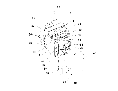
The junction box has a housing, which is made up of a lower
part 1 and an upper part 2. Lower part 1 and upper part 2 are
both one-piece, die-cast metal parts.
Lower part 1 of the housing is in the form of a box, the top
of which is open and the bottom of which is slanted like a desk.
The two narrow sides, the wide back, and the slanted, desk-like
bottom of lower part 1 are closed. The smaller side at the front
of lower part 1 is open and forms an insertion window for a
loading block, to be described later.
CA 02233119 1998-03-2~
Upper part 2 also has essentially the form of a box, the
bottom of which is open. The sides of upper part 2 are closed.
At the top of upper part 2, there is an arched roof, which is
open toward the front, and which serves to accept jacks, to be
described later.
When upper part 2 and lower part 1 are put together, the
upper edges of lower part 1 and the lower edges of upper part 2
engage along their two narrow sides and the wide back to form a
lock seam 3. The design of lock seam 3 prevents the formation of
a continuous gap at the joint between lower part 1 and upper part
2, through which high-frequency electromagnetic radiation could
pass.
The upper edge of the front of lower part 1 and
correspondingly the lower edge of the front of upper part 2
coming into contact with it are made thicker. In the middle of
the upper edge of the front of lower part 1, there is a
projection 4 with sides which slant upward toward each other.
When the housing is assembled, this projection engages a
correspondingly shaped recess 5 in upper part 2. A threaded hole
6 is provided in projection 4, into which a screw 7 fits, this
screw being seated in upper part 2. When the housing is put
together, screw 7 is turned in threaded hole 6 to draw upper part
2 and lower part 1 together and thus to bring them into
engagement. Two centering pins 8 are provided on top of the
front edge of lower part 1, one on each side of projection 4;
these pins fit into corresponding centering holes 9 in upper part
CA 02233119 1998-03-2~
2 so that upper part 2 and lower part 1 are guided precisely in
the axial direction during the assembly process.
On the back, two metal latching springs 10 are also provided
to ensure a reliable connection between lower part 1 and upper
part 2. Latching springs 10 are leaf springs, each of which has
bent-out catches 11 at the upper and lower ends. On the inside
surface of the back of lower part 1, two holding pockets 12 are
provided; when latching springs 10 are inserted from above into
these pockets, they are able to lock themselves in position by
means of their lower catches 11. When upper part 2 is set down
onto lower part 1, latching springs 10 serve as guides for upper
part 2 in the area of back wall and ultimately lock themselves by
their upper catches 11 in latching windows 13 in the back wall of
upper part 2.
A loading block 14 can be pushed into the open front of
lower part 1. Loading block 14 is made of plastic and is
essentially in the form of a rectangular block. Receiving holes
15, which are arranged in two offset rows, one above the other,
are provided in the front surface of loading block 14. These
holes extend into loading block 14 in the direction perpendicular
to the front surface. Contact ch~nnels 16 are provided in the
top of loading block 14; these channels extend into loading block
14 in the direction perpendicular to the top surface. Contact
channels 16 are arranged in two offset rows in such a way that
each contact channel 16 intersects a receiving hole 15 in the
interior of loading block 14 at a right angle. Contact ch~nnPls
CA 02233119 1998-03-2~
16 have the form of slots, rotated by an angle of 45~ to the axis
of receiving holes 15.
At the rear of loading block 14, a latching projection 17 is
provided in the middle of the bottom side; this projection
extends toward the rear of the lower part 1 (see Figure 6) from
the bottom surface of the loading block. At the bottom of the
front of loading block 14 a collar 18 is formed, which projects
downward over the lower surface of loading block 14. Collar 18
has two receiving hollows 19 for the cables to be connected.
Along the line where collar 18 connects to the block, the collar
has three centering windows 20 a certain distance apart, which
correspond to centering projections 21, which are molded on lower
part 1 underneath the insertion window in lower part 1. When
loading block 14 is pushed into lower part 1, centering
projections 21 of lower part 1 fit into centering windows 20 of
loading block 14, so that the block is positioned precisely in
the lower part. Latching projection 17 engages behind an inner
transverse wall 22 in lower part 1, so that loading block 14 is
also positioned in the insertion direction and held in place
there.
A mounting plate 23 is inserted into the open bottom of
upper part 2; this plate seals off the open bottom of upper part
2. Insulation displacement contacts 24 are inserted into
mounting plate 23, which is made of plastic, in an arrangement
which corresponds to the arrangement of contact channels 16 in
loading block 14. Insulation displacement contacts 24 are
CA 02233119 1998-03-2~
accordingly arranged in two offset rows and are rotated by an
angle of 45~. When upper part 2 is placed onto lower part 1,
insulation displacement contacts 24 pass through contact ch~nn~l s
16 of loading block 14. A printed circuit board 25, which is
essentially equal in area to mounting plate 23, is seated on
mounting plate 23. Insulation displacement contacts 24 extend
upward beyond the mounting plate in the form of soldering pins
26. Soldering pins 26 pass through printed circuit board 25 and
are soldered to its conductive pathways. Latching hooks 27 on
the outer edge of mounting plate 23 engage in recesses in printed
circuit board 25 to position it and to hold in place on mounting
plate 23.
One or more jacks 28 are mounted on printed circuit board
25; in the exemplary embodiment illustrated here, two jacks 28
are provided. In the illustrated example, jacks 28 are designed
as "Western~ jacks, into which terminal plugs can be inserted.
Jacks 28 are mounted on printed circuit board 25 in such a way
that the direction in which the plugs are inserted into them is
at an angle of 45~ to the plane of printed circuit board 25.
Jacks 28 are seated by their soldering pins in holes 29 of
printed circuit board 25. By soldering these pins to the
conductive pathways of printed circuit board 25, the jacks are
connected to soldering pins 26 of insulation displacement
contacts 24. Jacks 28 are enclosed by a shield cover 30, which
also forms the ground contact of jacks 28. Shield cover 30 is
seated by pins 31 in printed circuit board 25 and is soldered by
these pins 31 to the ground tracks of printed circuit board 25.
CA 02233119 1998-03-2~
Mounting plate 23 with printed circuit board 25 and jacks 28
is inserted as a preassembled unit from below into upper part 2
and rivetted to it. This rivetted connection establishes the
ground contact between printed circuit board 25 and upper part 2.
Jacks 28 are thus located in the upper region of upper part 2
with its arched, roof-like configuration, and their insertion
openings are accessible through the open insertion side of upper
part 2.
A plastic cover 32 iS placed on upper part 2 of the housing.
Cover 32 encloses the upper area of upper part 2 but leaves the
open insertion side of jacks 28 free. On the two narrow sides,
cover 32 has sidepieces 33, molded on as one piece, which rest
laterally against upper part 2. Two latching windows 34 are
provided in each sidepiece 3 3; by means of these latching
windows, sidepieces 33 are able to snap onto catches 35, which
are molded externally on the narrow sides of upper part 2. Cover
32 iS pressed down from above onto upper part 2; latching windows
34 of sidepieces 33 are thus able to lock onto catches 35, SO
that cover 32 iS held firmly on the upper part. In addition,
outward-projecting latching springs 3 6 are molded on sidepieces
33, by means of which cover 32 and thus the entire junction box
can be snapped into the frame of an empty box, e.g., a flush
device box.
The openings in cover 32 leading to the insertion holes of
jacks 28 can be sealed off by dust flaps 37, which are mounted in
cover 32 in such a way that they can pivot around an axis and
CA 02233ll9 l998-03-2~
lock themselves into recesses 38 in the closed position by means
of catches 39. In addition, labelling pieces 40 can also be
locked into cover 32 to label the services a-ssigned to the
various jacks 28. In the exemplary embodiment illustrated here,
one of jacks 28 iS connected to a telephone network, whereas the
other jack 28 iS connected to a data network, each being
characterized by its own appropriate symbol.
When the preassembled unit is inserted into upper part 2,
jacks 28 are braced against projections 41 when they reach their
end position.
By means of a plastic strap 42, a pull-relief clamp 43 and
a shielding clamp 44 are attached to slanted, desk-like bottom of
lower part 1 in such a way that they cannot be lost. Pull-relief
clamp 43 and shielding clamp 44 are each designed as flexible
metal strips, which are parallel to each other and which can be
attached by screws to lower part 1. The bottom of lower part 1
and its open front are sealed off by a metal shield cover 45.
The upper edge of shield cover 45 engages under a catch 4 6 on
lower part 1; at the bottom, shield cover 45 iS bent over at an
angle, so that it fits under the bottom of lower part 1. In the
bent area, shield cover 45 has overlapping edges 47, on which
lugs 48 are provided, into which screws can be inserted; these
screws can be screwed into threaded holes 49 in the bottom
surface of lower part 1 to attach shield cover 45.
CA 02233119 1998-03-2~
The junction box shown with two jacks 28 iS for the
connection of two shielded cables 50. The cables are brought in
from the rear along the slanted, desk-like bottom surface of
lower part 1. Cables SO are positioned and held in place on
lower part 1 by pull-relief clamp 43. Pull-relief clamp 43 holds
cables 50 firmly by their insulation against the bottom of lower
part 1. Ahead of pull-relief clamp 43, the insulating outside
sheath of cables 50 iS removed, so that cable shielding 51 is
exposed. Cable shielding 51 iS pressed by shielding clamp 44
against the bottom surface of lower part 1 to establish good
ground contact between cable shielding 51 and the metal of lower
part 1. The forward end of cable shielding 51 lies in receiving
hollows 19 of collar 18 of loading block 14. At the forward end
of cables 50, cable shielding 51 iS removed, so that wires 52 are
exposed. Wires 52 are introduced into receiving holes 15 of
loading block 14 and contacted by insulation displacement
contacts 24, which pass through loading block 14.
To install the junction box, the first step is to expose
cable shielding 51 and wires 52 at the ends of cables 50. The
wires 52 are then introduced into receiving holes 15 of loading
block 14 while loading block 14 iS still outside the housing,
which means that wires 52 can be inserted without encumbrance.
Then loading block 14, with wires 52 inserted in it, is pushed
into lower part 1 and latched in place. Now cables 50 are fixed
in place on lower part 1 by means of pull-relief clamp 43, and
cable shielding 51 iS brought into contact with lower part 1 by
means of shielding clamp 44. Then upper part 2 iS set down onto
CA 02233ll9 l998-03-2~
lower part 1, and thus insulation displacement contacts 24 enter
contact chAnnels 16 and pass through loading block 14. Centering
pins 8 and centering holes 9 make it easy to place upper part 2
precisely onto lower part 1 and thus to introduce insulation
displacement contacts 24 into contact channels 16. Screw 7 is
then tightened in threaded hole 6, as a result of which upper
part 2 iS drawn against lower part 1. Thus insulation
displacement contacts 24 travel all the way through contact
channels 16 until they make contact with wires 52. Because of
the pitch of the threads of screw 7, it does not take much force
for the insulation displacement contacts 24 to cut through the
insulation of wires 52. As soon as lower part 1 and upper part
2 have been drawn firmly together by screw 7, lower part 1 and
upper part 2 form a closed, metal housing, which surrounds and
shields jacks 28, printed circuit board 25, and insulation
displacement contacts 24 in loading block 14. The free area of
wires 52 between cable shielding 51 and loading block 14 iS
shielded by shield cover 45, which is set on top. The shielding
is carried through with good electrical contact from cable
shielding 51, via shielding clamp 44, lower part 1, upper part 2,
and printed circuit board 25 to the shielding of jacks 28. The
completely assembled junction box is then inserted into an empty
electrical box and locked in place by means of latching springs
36.
Figures 8-10 show a modified design of the junction box.
Only lower part 1 and upper part 2 are shown. Otherwise, this
design is the same as the design described above according to
CA 02233ll9 l998-03-2~
Figures 1-7, and therefore reference can be made to that extent
to the preceding description.
~ When lower part 1 and upper part 2 are drawn together by
means of screw 7, insulation displacement contacts 24 pass
through loading block 14 and cut through the insulation around
wires 52. The insulation of wires 52 offers a certain mechanical
resistance to this penetration. Because the screw is located
asynunetrically outside loading block 14 and insulation
displacement contacts 24, this resistance can cause a tipping
moment to act on upper part 2, which can in turn interfere with
the penetration of the insulation of wires 52 by insulation
displacement contacts 24.
To counteract this interference, a downward-pointing strap
53 iS molded on the back of upper part 2, opposite screw 7.
Strap 35 engages in a guide opening 54 in the back of lower part
1. Catches 55 are provided at both edges of guide opening 54.
Recesses 56 provided in the edges of strap 53 fit these catches
55. In the center of guide opening 54, a deep groove 57,
extending longitll-l;n?,lly, iS provided. At its upper end, this
groove has a support edge 58. An opening 59, which is
essentially aligned with support edge 58 of groove 57 after lower
part 1 and upper part 2 have been brought together, is provided
in the middle of strap 53. In the process of assembly, upper
part 2 iS set down onto lower part 1, starting from the position
shown in Figure 8. Upper part 2 iS guided by centering pins 8,
which engage in centering holes 9 and also by strap 53, which
14
CA 02233119 1998-03-2~
engages in guide opening 54. By means of screw 7, which engages
in threaded hole 6, upper part 2 is drawn against lower part 1,
and insulation displacement contacts 24 thus pass through contact
channels 16 in loading block 14. The resistance offered to the
cutting of the insulation around wires 52 by insulation
displacement contacts 24 and the asymmetric arrangement of
threaded hole 6 and screw 7 in relationship to loading block 14
have the result that, even after screw 7 has been completely
screwed into threaded hole 6, upper part 2 is still not fully
seated on lower part 1 at the back, opposite screw 7. This
situation is shown in Figure 9.
After screw 7 has been screwed completely down in threaded
hole 6 and upper part 2 has assumed the position shown in Figure
9 with respect to lower part 1, a screwdriver 60 is introduced
through opening 59, so that the tip of screwdriver 60 fits into
groove 57 and is supported against support edge 58. Screwdriver
60 can then be pivoted downward, as shown by the arrow in Figure
10. Whereas the tip of screwdriver 60 is thus supported by
support edge 58, the area of screwdriver 60 behind the tip is
braced against the lower edge of opening 59. When screwdriver 60
is tilted down, therefore, strap 53 is pushed farther down until
edge recesses 56 on strap 53 lock onto catches 55, as indicated
in Figure 10. The levering action of screwdriver 60 thus
overcomes the resistance to the cutting of the insulation of
wires 52 by insulation displacement contacts 24. Upper part 2 is
seated firmly all the way around on lower part 1 as soon as the
edge recesses 56 of strap 53 have locked onto catches 55.
CA 02233119 1998-03-2~
To remove upper part 2 from lower part 1, screwdriver 60 is
pushed from below into groove 57 between strap 53 and lower part
1, so that strap 53 can be lifted by the levering action of
screwdriver 60 out of guide opening 54 and edge recesses 56 can
be released from catches 55.
16