Some of the information on this Web page has been provided by external sources. The Government of Canada is not responsible for the accuracy, reliability or currency of the information supplied by external sources. Users wishing to rely upon this information should consult directly with the source of the information. Content provided by external sources is not subject to official languages, privacy and accessibility requirements.
Any discrepancies in the text and image of the Claims and Abstract are due to differing posting times. Text of the Claims and Abstract are posted:
| (12) Patent Application: | (11) CA 2233358 |
|---|---|
| (54) English Title: | PROCESS FOR MAINTAINING THE MICROSYNCHRONOUS OPERATION OF DUPLICATED INFORMATION-PROCESSING UNITS |
| (54) French Title: | PROCEDE DE MAINTIEN DU FONCTIONNEMENT MICROSYNCHRONE D'UNITES DOUBLEES POUR LE TRAITEMENT D'INFORMATIONS |
| Status: | Deemed Abandoned and Beyond the Period of Reinstatement - Pending Response to Notice of Disregarded Communication |
| (51) International Patent Classification (IPC): |
|
|---|---|
| (72) Inventors : |
|
| (73) Owners : |
|
| (71) Applicants : |
|
| (74) Agent: | SMART & BIGGAR LP |
| (74) Associate agent: | |
| (45) Issued: | |
| (86) PCT Filing Date: | 1996-09-26 |
| (87) Open to Public Inspection: | 1997-04-10 |
| Examination requested: | 2003-07-31 |
| Availability of licence: | N/A |
| Dedicated to the Public: | N/A |
| (25) Language of filing: | English |
| Patent Cooperation Treaty (PCT): | Yes |
|---|---|
| (86) PCT Filing Number: | PCT/DE1996/001843 |
| (87) International Publication Number: | WO 1997013203 |
| (85) National Entry: | 1998-03-27 |
| (30) Application Priority Data: | ||||||
|---|---|---|---|---|---|---|
|
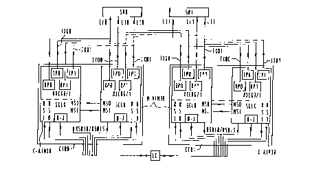
The units (CTR0, CTR1) are under the influence of mutually independent clock
pulses (SCLK, RXCK). In order to prevent the loss of microsynchronization when
information is transferred from one clock system to another, and owing to
different error situations as concerns the information received by the units,
the information received is stored temporarily before being passed on for
processing or the processing result information is stored temporarily before
being emitted. If reception is error-free, the units are cross-synchronized.
If, owing to faulty reception, a synchronous signal fails in the case of one
partner unit, this unit rejects the information received despite the fact that
it is error-free.
Les unités (CTRO, CTR1) sont sous l'influence d'impulsions de synchronisation (SCLK, RXCK) indépendantes les unes des autres. Pour prévenir la perte de la microsynchronisation lors du transfert d'informations d'un système d'horloge vers l'autre système d'horloge et, en cas d'erreurs diverses, lors de la réception d'informations par les unités, sont mémorisées provisoirement les informations reçues avant leur retransmission pour traitement ou bien les résultats de traitement avant leur émission. Dans le cas d'une réception exempte d'erreurs, les unités émettent un signal de synchronisation et il y a une synchronisation croisée des unités. En l'absence d'un signal de synchronisation du côté de l'unité associée, l'unité concernée rejette les informations reçues au même titre que lors d'une réception entachée d'erreurs, et ce, même si les informations sont exemptes d'erreurs.
Note: Claims are shown in the official language in which they were submitted.
Note: Descriptions are shown in the official language in which they were submitted.
2024-08-01:As part of the Next Generation Patents (NGP) transition, the Canadian Patents Database (CPD) now contains a more detailed Event History, which replicates the Event Log of our new back-office solution.
Please note that "Inactive:" events refers to events no longer in use in our new back-office solution.
For a clearer understanding of the status of the application/patent presented on this page, the site Disclaimer , as well as the definitions for Patent , Event History , Maintenance Fee and Payment History should be consulted.
| Description | Date |
|---|---|
| Inactive: IPC expired | 2013-01-01 |
| Application Not Reinstated by Deadline | 2006-06-14 |
| Inactive: Dead - Final fee not paid | 2006-06-14 |
| Inactive: IPC from MCD | 2006-03-12 |
| Inactive: IPC from MCD | 2006-03-12 |
| Deemed Abandoned - Failure to Respond to Maintenance Fee Notice | 2005-09-26 |
| Deemed Abandoned - Conditions for Grant Determined Not Compliant | 2005-06-14 |
| Notice of Allowance is Issued | 2004-12-14 |
| Letter Sent | 2004-12-14 |
| Notice of Allowance is Issued | 2004-12-14 |
| Inactive: Approved for allowance (AFA) | 2004-11-15 |
| Amendment Received - Voluntary Amendment | 2004-10-21 |
| Inactive: S.30(2) Rules - Examiner requisition | 2004-05-05 |
| Letter Sent | 2003-08-26 |
| Request for Examination Received | 2003-07-31 |
| Request for Examination Requirements Determined Compliant | 2003-07-31 |
| All Requirements for Examination Determined Compliant | 2003-07-31 |
| Inactive: IPC assigned | 1998-07-02 |
| Classification Modified | 1998-07-02 |
| Inactive: First IPC assigned | 1998-07-02 |
| Inactive: Notice - National entry - No RFE | 1998-06-09 |
| Application Received - PCT | 1998-06-08 |
| Application Published (Open to Public Inspection) | 1997-04-10 |
| Abandonment Date | Reason | Reinstatement Date |
|---|---|---|
| 2005-09-26 | ||
| 2005-06-14 |
The last payment was received on 2004-08-12
Note : If the full payment has not been received on or before the date indicated, a further fee may be required which may be one of the following
Please refer to the CIPO Patent Fees web page to see all current fee amounts.
| Fee Type | Anniversary Year | Due Date | Paid Date |
|---|---|---|---|
| Registration of a document | 1998-03-27 | ||
| Basic national fee - standard | 1998-03-27 | ||
| MF (application, 2nd anniv.) - standard | 02 | 1998-09-28 | 1998-08-17 |
| MF (application, 3rd anniv.) - standard | 03 | 1999-09-27 | 1999-08-12 |
| MF (application, 4th anniv.) - standard | 04 | 2000-09-26 | 2000-08-18 |
| MF (application, 5th anniv.) - standard | 05 | 2001-09-26 | 2001-08-16 |
| MF (application, 6th anniv.) - standard | 06 | 2002-09-26 | 2002-08-16 |
| Request for examination - standard | 2003-07-31 | ||
| MF (application, 7th anniv.) - standard | 07 | 2003-09-26 | 2003-08-14 |
| MF (application, 8th anniv.) - standard | 08 | 2004-09-27 | 2004-08-12 |
Note: Records showing the ownership history in alphabetical order.
| Current Owners on Record |
|---|
| SIEMENS AKTIENGESELLSCHAFT |
| Past Owners on Record |
|---|
| HELMUT BRAZDRUM |
| RUSSELL HOMER |

