Note: Descriptions are shown in the official language in which they were submitted.
CA 02233526 1998-03-30
FLOOD 1-2-3-4-2
OPTICAL AMPLIFIER DESIGNS FOR MULTICHANNEL
FIBER OPTIC: COMMUNICATION NETWORKS
BACKGROUND OF THE INVENTION
This invention relates to multichannel fiber optic communication
networks, and is more particularly concerned with optical amplifier designs
for
such networks that provide a substantial cost saving through the use of
identical components in amplifiers having different functions within a
network.
Optical amplifiers must satisfy a number of rigorous technical
requirements in order to assurE~ reliable and accurate communications within a
fiber optic network. As such, trey typically represent a significant component
of
the overall network cost. An irndividual optical amplifier may cost tens of
thousands of dollars, and a given network may require a large number of such
amplifiers.
Amplifiers for metropolitan area networks (MANs) or metro amplifiers, for
example, have special requirements related to operation over multiple
wavelength channels, including input and/or output power monitoring, constant
output power (constant averagE~ gain per channel), gain flatness over a wide
wavelength band, and telemetry monitoring (also referred to as supervisory
channel monitoring) - all with the need to support significant passive loss.
All
of these requirements must be met at a relatively high output power and
moderate noise figure in order t:o meet stringent systems requirements.
CA 02233526 1998-03-30
2
Traditionally, optical amplifiers have been designed with a particular
focus on their location and function within a network - for example, node
input amplifier, node output amplifier, or line amplifier - without regard to
the
other amplifiers in the network. This individualized design approach is a
major
contributing factor to the high cost of optical amplifiers.
Doped-fiber optical amplifiers utilize lengths of optical fiber doped with
an element (rare earth) which can amplify light, the most commonly used of
such elements being erbium. another element receiving considerable attention
is praseodymium. The doped 'fiber is driven or "pumped" with laser light at an
appropriate frequency which e:~ccites electrons within the fiber to produce a
population inversion of electrons between high and low energy states. Photons
of light from a data signal supplied to the doped fiber stimulate the excited
electrons to release more photons, thereby amplifying the data signal.
Because doped-fiber amplifiers do not amplify all light wavelengths
equally (that is, they do not provide a perfectly flat gain spectrum) it is
necessary to employ gain flattening filters to flatten the gain spectrum.
These
filters are designed to minimize gain ripple at a predetermined average
inversion of the doped fiber (referring to the average inversion over the
length
of the fiber) and at a predetermined internal gain of the amplifier (referring
to
the minimum gain provided by the fiber among the gains for different
wavelengths of the system). The process for designing gain flattening filters
is
time consuming and expensive, and the filters themselves are expensive as
well. Gain flattening filters thu:c represent a substantial component of the
cost
of multi-channel fiber optic amplifiers.
DISCLO~>URE OF THE INVENTION
The present invention, in contrast to the traditional, individualized design
approach, is based on an approach which takes amplifiers of different
functions
into consideration simultaneously. The invention can thus provide a family of
multi-channel optical amplifiers that utilize substantially identical
components,
especially the gain flattening fili:er, for amplifiers having different
functions (e.g.,
node input amplifier, node output amplifier, andlor line amplifier).
CA 02233526 1998-03-30
3
Briefly stated, in accordance with the present invention, amplifiers for
different functions and having predetermined net gains are constructed to have
total insertion losses such that their respective internal gains (internal
gain =
net gain + total insertion loss) can be made substantially the same - that is,
as close to each other as practicable, preferably within about 1.5 dB, and
more
preferably within 1 dB. By so <;onstructing the amplifiers, it becomes
possible
to use identical gain flattening filters within the different amplifiers
without
undue degradation of gain flatness.
With amplifier designs as just described, the gain flattening filter may be
designed for operation at an internal gain midway between the highest and
lowest internal gains (highest and lowest minimum internal gains) of the
amplifier family at a predetermiined average inversion. In a particular
amplifier,
therefore, the filter will be operated at an internal gain that can be no more
than
one half the difference between the highest and lowest internal gains of the
amplifier family. Thus, when the internal gains are within the aforementioned
range of 1.5 dB, a filter designed for operation at the midpoint of the range
would operate at a difference of no more than + .75 dB from the design value.
More preferably, however, the filter should be operated within ~ .5 dB of its
design value, corresponding to the aforementioned 1 dB range, for better gain
flatness.
SUMMARY OF THE INVENTION
Briefly stated, in accordance with one of its basic aspects, the present
invention provides a multichannel fiber optic communication network,
comprising a plurality of nodes interconnected via fiber optic links, at least
one
of the nodes having a multichannel input optical amplifier and a multichannel
output optical amplifier, one of 'which is connected to a multichannel line
amplifier via a fiber optic link of the network, wherein each of at least two
of the
input, output, and line amplifiers is a doped-fiber amplifier and includes a
gain
flattening filter, the two amplifiers are constructed to have total insertion
losses
such that their respective internal gains at a predetermined inversion are
CA 02233526 1998-03-30
4
substantially the same, and thE~ gain flattening filters of the at least two
amplifiers are substantially identical.
According to another basic, but more specific aspect, the present
invention provides a multichannel fiber optic communication network,
comprising a plurality of nodes interconnected via fiber optic links, at least
one
of the nodes having a multichannel input optical amplifier and a multichannel
output optical amplifier, one of which is connected to a multichannel line
amplifier via a fiber optic link of the network, wherein each of at least two
of the
input, output, and line amplifiers includes first and second doped-fiber gain
stages in series and a gain flattening filter intermediate the gain stages,
the two
amplifiers are constructed to have total insertion losses such that their
respective internal gains at a predetermined inversion a re substantially the
same, and the gain flattening filters of the at least two amplifiers are
substantially identical.
BRIEF DESCRIPTION OF THE DRAWINGS
The aforementioned aspects of the invention, as well as its various
features and advantages, will be more fully appreciated upon considering the
following detailed description off the preferred embodiments in conjunction
with
the accompanying drawings, in which:
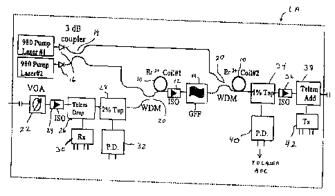
Figures 1-3 are diagramimatic illustrations showing a multichannel line
amplifier, input amplifier, and output amplifier, respectively, constituting
an
amplifier family in accordance vvith the present invention;
Figures 4-6 are plots showing measured gain flatnesses of a line
amplifier, an input amplifier, and an output amplifier, respectively,
constructed
in accordance with the invention; and
Figure 7 is a diagrammatic illustration showing a 32-channel wavelength
add/drop network node incorporating the input and output amplifiers of Figures
2 and 3.
CA 02233526 1998-03-30
DESCRIPTION OF THE PREFERRED EMBODIMENTS
Figures 1-3 diagrammatically illustrate a family of multichannel metro
amplifiers in accordance with the present invention. The illustrative
amplifiers
5 employ erbium-doped fiber amplification, which provides substantial gain for
channel wavelengths in a range from about 1530 to about 1560 nm. The
number of channels or wavelengths on the network will naturally depend upon
the requirements of a particular installation, but a typical network is likely
to
operate at 16 or 32 channels within the aforementioned wavelength band. It
will be understood, of course, that the illustrative amplifier designs are
merely
exemplary and that the basic principles of the present invention are not
limited
i:o MAN applications or to the use of erbium-doped fiber amplification.
Figure 1 shows the construction of a line amplifier LA. In the form
shown, the line amplifier includes two erbium-doped gain stages 10 connected
in series by way of an optical i~;olator 12 and a gain flattening filter 14.
The
gain stages, which are constituted by respective coils of erbium-doped fiber,
are redundantly pumped by a pair of 980 nm laser diodes 16 coupled to the
gain stages by a 2 x 2 3dB coupler 18. The outputs of the coupler 18 are
coupled to the respective gain :stages 10 via WDM (wavelength division
rnultiplex) couplers 20, which combine the pump light with the signal light to
be
amplified. Although not strictly necessary in the practice of the invention,
the
dual- pumpldual-gain-stage arrangement just described is advantageous in the
MAN context, since it allows for' continued operation of the amplifier in a
"soft-
fail" mode in the event of a failuire of one of the pump sources.
The gain flattening filter 14 is preferably of the thin film type. The filter
rnay be transmissive or reflective, although a transmissive filter may be
preferred for ease of incorporation into the amplifier structure. Thin film
filters
offer advantages relative to ma:;s producability, temperature stability, and
well-
developed packaging. Other types of gain flattening filters which may be used
include long period gratings, tapered fiber gratings, and acousto-optic
filters.
Ahead of the first gain stage, which is the left gain stage 10 in Figure 1,
the input stage of the amplifier includes a variable optical attenuator 22, an
CA 02233526 1998-03-30
6
optical isolator 24, a telemetry or supervisory channel drop unit 26, and a 2%
power tap 28. The variable optical attenuator operates to compensate for
changes in link span loss (suclh as with temperature) between the amplifier
and
a previous node or line amplifier in the network, thereby maintaining a
substantially constant link span loss ahead of the amplifier. The variable
optical attenuator can be controlled by various techniques, as will be
appreciated by those skilled in the art. For example, the control may be
effected from a central office based on information received over the
:supervisory channel. The initial setting of the attenuator 22 would be made
in
accordance with the design link span loss. If desired) the initial setting of
the
attenuator can have two components, namely) a first component designed to
provide a desired insertion loss in the amplifier and a second component
determined based on the link span loss. In this way, the attenuator can be
used for the combined purposes of providing a desired insertion loss of the
amplifier and to compensate changes in link span loss.
The telemetry drop unit 26 extracts the supervisory signal (e.g., a 2 Mbs
' signal at a wavelength slightly out of the communication band) from the
signal
input to the amplifier. The extracted signal is input to a receiver 30, the
output
of which can be supplied to they network central office by suitable means.
Supervisory monitoring techniques are known in the art and therefore will not
be addressed further herein.
The 2% power tap 28 has its monitor output connected to a
photodetecting unit 32 which detects the power level of the input signal to
the
amplifier. The power level may be indicated by photodiodes within the unit,
which are driven in accordance with the power monitor signal. The output of
the photodetecting unit may be used to generate an alarm in the event of a
system fault, for example. It may also be used as a parameter for controlling
pump power in order to control the output power of the amplifier to a constant
level.
While the arrangement of the input stage components may be changed
from that shown in Figure 1, thE~ illustrative arrangement, with the variable
optical attenuator ahead of the telemetry channel drop unit 26 and power tap
CA 02233526 1998-03-30
7
28 is advantageous to achieve a near constant power on the telemetry channel
drop unit and input power monitor photodiodes. This permits greater ease in
linearization of the photodiodHS and improved bit error rate performance of
the
telemetry channel drop signal because of the near constant power on these
components despite varying link span losses.
Beyond the second gain stage of the amplifier, the output stage includes
a 1 % power tap 34, an optical isolator 36, and a telemetry or supervisory
channel add unit 38, which are connected in series with the output of the
second gain stage, preferably in the order shown. The monitor output of the
1 % tap unit is supplied to a photodetecting unit 40, the output of which is
coupled to an electrical automatic gain controller, as indicated, to control
the
pump lasers 16 so as to maini:ain a substantially constant output power level
of
the amplifier.
The telemetry add unit 38 combines a supervisory signal supplied from a
transmitter 42 with the commuinication signal for transmission to the next
amplifier in sequence, which may be another line amplifier or a node input
amplifier.
Figure 2 shows the construction of the node input amplifier IA. This
amplifier has the same basic construction as the line amplifier shown in
Figure
1, except that the output stage does not include the optical isolator 36 or
the
telemetry add unit 38 and its associated transmitter 42. These components are
unnecessary since the input amplifier does not have its output connected
directly to another fiber optic link of the network.
Figure 3 shows the output amplifier OA. The construction of this
amplifier is basically the same as that of the line amplifier in Figure 1,
except
that the input stage does not include the variable optical attenuator 22, the
optical isolator 24, or the telemetry drop unit 26 and its associated receiver
30.
These components are unnecfasary since the input stage is not connected
directly to a fiber link of the network.
Figure 7 is a diagram dE~picting how the amplifiers of Figures 1-3 can be
incorporated in a metropolitan area network (MAN) having 32 communication
channels or wavelengths ~,1 - u32 and a supervisory channel ~,S. Figure 7
CA 02233526 1998-03-30
8
shows an exemplary node N vrhich includes an input amplifier and an output
amplifier coupled via a splitter arrangement, a set of four wavelength
addldrop
multiplexers (which constitute a switch matrix), and a combiner arrangement.
Each of the input and output amplifiers is linked to another node of the
network
via a line amplifier, as shown. For two-way communication, the node also
includes an identical arrangement (not shown) having an opposite transmission
direction and coupled to the other nodes via two additional fiber links and
line
amplifiers (not shown).
All of the signal channells ~,1 - x,32 and the supervisory channel ~.S are
input by the input amplifier of the node. The input amplifier extracts the
supervisory channel as previously described and outputs the amplified channel
:signals ~,1 - x,32 to the splitter arrangement. The splitter arrangement
splits the
channels into four wavelength bands ~,1 - ~,8, ~.9 - x.16, 717 - x.24, and
x,25 -
;~,32 which are input to respective wavelength add/drop multiplexers, only one
of which (designated M) is fully illustrated in Figure 7 for the sake of
convenience. Each of the wavelength addldrop multiplexers includes a 1 x 8
demultiplexer which demultiplexes the signals of the corresponding wavelength
band and passes them through a corresponding set of switches which may be
configured either to pass the corresponding channel signal undisturbed or to
extract it and replace it with a clifferent signal on the same wavelength. The
signals from the switches are input to an 8 x 1 multiplexer which recombines
the signals. The outputs of the multiplexers are passed to a combiner
arrangement which recombines the four wavelength bands and outputs them
together to the output amplifier, where they are amplified and supplemented
with the supervisory signal for transmission to the next node.
E=xamples
Tables 1-3 show design parameters of the metro amplifiers in Figures 1-
3 for application in a MAN as shown in Figure 7. These designs were tested by
computer simulation for operation at 16 and 32 channels at an effective
average inversion N2 = .65. All components of the amplifiers represented in
the tables are commercially available components with the exception of the
gain flattening filter (which had to be designed for this particular
application),
CA 02233526 1998-03-30
9
and they were selected to provide appropriate insertion losses such that the
internal gains of the amplifiers would be within a range of 1 dB.
The coil lengths of the individual gain stages can be set to obtain the
best balance of gain flatness (given a particular gain flattening filter),
noise
figure, and pump power. Appropriate lengths can be determined empirically or
by simulation. In the illustrative examples, it was determined that the first
stage
coil should be approximately .55 of the total length of the two coils.
Table 4 shows the desi~~n parameters for the gain flattening filter, which
is preferably a transmissive, thin film type filter as noted earlier. As shown
in
Table 4, the gain flattening filter was designed for operation at 17.92 dB,
which
is the midpoint between the internal gains of the input and output amplifiers.
Tables 5 and 6 show the simulation results. For purposes of the
simulation, the following conditions were taken to apply:
1. Insertion loss values of all components and splices are manufacturing
mean values indicated in Tables 1-3.
2. Total signal input power is evenly distributed over the 32 channels at
'the input of the input amplifier and the line amplifier for 32 channel
operation.
For 16 channel operation, the itotal signal input power is evenly distributed
over
16 channels within the 1545-1!560 nm spectral band.
3. Computed pump power values take into account the penalty incurred
due to pump connectors (0.5 dB) and the 3 dB soft-fail coupler insertion
losses
(0.2 dB excess).
4. Average inversion N2 = 0.65.
CA 02233526 1998-03-30
Table 1
Power Budget two stages Line Amplifier with Electrical AGC (13 dB Net Qain)
Target Net Gain(dB) 13
passive Loss (dB)
mean a Mean +a
Input tOSa
Connector -0.15 0.1 -0,25
S lice: emf-srnf-0.03 0.03 -0.06
Isolator -0.4 0.03 -O.a3
5 lice: smf-smf-0.03 0.03 -0.06
VOA -1 0.5 -1.5
S lice: smf-smf-0.03 0.03 -0.06
SC. dro -0_35 0.12 -0.s7
S tics: smf-srrtf-0_03 0.03 -0.06
2% to -0_ 18 0.03 -0.21
S lice: smf-smf-0.03 0.03 -0.08
980/1550 wdm -0.28 0.05 -0.33
S lice: G3-Er -O.os 0.03 -0.os
total in ut -2.57 _ -3.58
loss 1.01
int~rst~ a loss
S lice: Er-smf ~ -0,2 0,03 -0.23
Isolator -0.4 0.03 -0_43
5 lice: smf-smf-0.03 0.03 -0.06
GFF excess toss-0.5 0.3 -0.8
S_tice: smt-smf-0.03 0.03 -0.06
98011550 wdm -0.28 0,05 -0.33
S Ilce: G3-Er -0.06 0_03 -0,09
total intesta -t.5 0.5 -2
a toss
~utam iau
S lice: Er-smt -0.2 D_o3 -x.23
1 ~ to -0.13 0,03 -0.16
S Ilce: smf-smf -0.03 0.03 -0.06
SC, Add -0,43 0.08 -0_51
.. .. S lice: smf-smf -0.03 0.03 -0.OB
. y_---__ .
Isolator .a 0.03 -O.d3
O -
total out ut -1.22 0,23 -1.5
loss
Total asslv Ions-5.29 _ -7.03
1.74
Total EI'blrvnl 18.29 T 20.03
In
rower tsuaget 5ummasy
Passive Loss (d Powerlch (dBm) Powerlchan (d8m)
/Tl~a'~rl W fU~GaR 1 A fl~a~n L/sew i i
In ut ower/ch -13 -13
In ut. Loss _ -3.58 -15.57 -16.58
-2.57
intersta a loss -1.5 _ -2 -t7.07 -18.58
Out ~.rt toss -1.22 -1.a5 -18.29 -20.03
Er coin ain 1 a.2s 20.03 0 0
c = 1 s;and2rd de~.~i~Tion
CA 02233526 1998-03-30
11
'Table 2
Power budget: two stages Inaut
Ampti(ier with Electrical
AGC
(14 d6 Net Olin)
Target Net Gain(dB)
td
Passive toss
(dl3)
mean a Mean t Q
tn ut loan
Connector -0.15 0.7 -025
S lice: smf-smf -0.03 0.03 -0
06
Isolator -0.4 0.03 ,
-0.d3
S lice: smf-smf -0.03 0.03 Ø06
VOA -t 0.5 -1
5
S lice: smf-smf -0.03 0.03 .
-p
Og
SC. d ro -0.35 0. .
7 -0
2 47
S tlce: smf-smf -0.03 0_03 .
-0_06
2"/o to -0.18 0.03 -0
2i
S lice: smf-smt -0.03 0.03 .
~ .p,p6
980/1550 wdm -0.28 0.05 -0
33
S lice: G3-Er 0.05 0.03 .
-0
pg
total tn ut Loss -2.57 1 .
_Oi -3
58
Intecsta s loss .
S lice: Er-smf -0.2 0.03
Isolator -0.4 0.03 -O.d3
S lice: smf-smf -0.03 0.03 -0.08
GFF excess loss -0.S 0.3 -0.8
S lice: smf-8mrf -0.03 0.03 -O.Q6
980/1550 wdm ~ -0.28 0.05 -0
S lice: G3-Er -0.06 0.03 -0.09
total inte3ta a loss -1.5 0.5
Output toga
. ~.-~.... ~.2 0.03 -023
i % is ~ -0.13 0.03 -0.16
total ou ut loss -0.33 0.08 -0
- Total asslve (vss -4.4 1.57 -5.97
Total Erblum In 1e.4
Power Budget Summary
Passive Loss Power/chgn (dBm)
(d
Power/ch
(dBm)
mean Mean
+ a
mean
Monr
~ .'
m u~ uw8r~G1 -13 -13
!n ut. Loss -2.57 -3.58 -15.57 -16.58
intersta a loss -1.5 -2 -17_07 -18,58
Out ut loss -0.33 -0_39 -17.4 -18.97
Er coil ain ~ 18.4 19.9T 1 i
6 = 1 standard deviation
CA 02233526 1998-03-30
12
Table 3
Power Budget: two stages output Amplifier with Electrical AGC (1''t dB Net
Gain)
Target Net Gain(dB) 14
Passive Loss (dB)
mean c Mean + Q
.__....___
Connector -0.15 0.1 -0.25
S lice: smf-smf -0.03 0.03 -0.06
2.6 to -0,18 0.03 -0.21
S lice: smf-smf -0.03 0.03 -0.06
980/1550 wdm -0.28 0.05 -0.33
$ lice: G3-Er -0.06 0.03 -0.09
total in ut loss-0.73 0.27
_~___ .___
....v. v.a ~
... -0.2 0.03 -0.23
S lice: Er-smf
Isolator -0.4 0.03 -0.43
S lice: smf-amt -0.03 0.03 -0.06
GFF excess toss -4.5 0.3 -0_8
S l(ce: smf-smf -0.03 0.03 -0.06
98011550 wdrn _-0.28 0.05 -0.33
S Irce: G3-Er -0.06 0.03 -0.09
total Intesta -1.5 0.5 -2
a loss
vi1 W .vv~
S lice: Er-smf -0.2 0.03 -0.23
1 % t -0. l 3 0.03 -0.18
S lice: smf-smf -0.03 0.03 -0.06
SC. Add -0.43 0.08 -0.51
S lice: smf-smf -0.03 0.03 -0.06
isolator -0.4 0.03 -0.43
total ou ut loss-122 0.23 -1.45
Totsl esstve -3.45 1
loaa
Total rbturtt lT.dS 18r46
ie
Power Budget Summary
Passive Loss (d Powerlch (dBm) Powerlct~an (dBm)
- ~o~,~ .a. ~ mean Mean + a
.. ~ca..
-14 14
v I n ut rrerlch -1 73 -15
-14
In ut. Loss -0.73 . 17
intersta a -1.5 -2 -16.23-
loss
Out ut loss -1.22 -1.45 -17.d5-18.45
Er coil gain- 17.45 18.45 0 0
c = ' standard cievia~on
CA 02233526 1998-03-30
13
Total Erbium Length (m) 13,7~g Table 4 _
Effective average inv N2 ~ 0.65
Minimum Internal Gain (dB) 17_92
Wavelength g_eff alpha_effGain ene~cient Erbium Gain
(dB/m) (dB)
1559.79 4.9590681 _ 1.41645339 19.48842267
1685
1558.98 5_0135591.18 1.430677966 19.684 t 3299
1558.17 5.1272031.1805 1.436860169 19_76919149
1557.36 5.2327971.1835 1.445139831 19.88310807
1556.55 5.3371191 _179 1.445855932 19,89296064
1555.75 5.366-0411.182 - 1.450322034 19.95440796
1554.94 5.443391.178 1.448169492 19.924797
98
1554.13 5.5472881 _169 1.446364407 19.89995654
1551,72 5.7331361.1555 1.44215678 19.84206546
1550.92 5.8020341.152 1.442101695 7 9.84130757
1550.12 5.8500851.1455 1 _438004237 19.78493227
1549.32 5..941611.1355 1.432580'508 19, 710309321
154.8.51 6.0246611.1255 1.426733051 19_62985846
1547.72_ 6.0538141.1175 1.420190678 1 s.s3984254
1546.92 6.0840681.106 7 .41020339 19.40243139
j
7 546_12 6_2125421.094 1.404627119 19.32570968
1543.73 6.3878811.0485 1.367894068 18.82031414
1542.94 6.4.31 1.034 1.355559322 18.85060524
t 86
1542.14 8.4621191,01 1.339605932 18.43110886
B5
1541.35 6.5188981.0015 1.327444915 18.26379023
1540.56 6.5806780.986 1 _315033898 18_09303195
1539.77 6.6778810.9695 1.303394068 17.93288412
1538.98 6:8491530.96 1 _302457627 17.92
1538.19 6.9851690.9625 1 _311758475 18.04796669
1535.82 8.1372881, 01 1.416884.407 19.49407769
1535.04 8.5530511 _043 1.470652542 20.2341274
1534.25 9.076611.072 1.525830508 20.99329924
1533.47 9_4813561.09 1 _564067797 21.51939098
1532,68 9.7699151.0925 1.580995763 21 _75229618
1531.9 10.015511.0815 1 _582275424 21 _76990253
1531.12 10.140341.058 1.565016949 21.53245
1530.33 10_176781.023 1_531838983 21.07596747
4.959068 1.302457627 17.92
.. ~ 21.76990253
Gain Riple (dB) 3.849902531
* (2) The fiber leagth ie appropriate for Corning
Er2128(5-2128-202).
'* Wavelength valueB are defined in vacuum
*+~ g_eff and alpha_eff are effective Giles like
parameters. But rigorously these are not strictly
equivalent to g' and alpha usually defined. These
parameters have been derived using the 5+ probe technique to
mimic a 32 ehannele~ loading configuration.
CA 02233526 1998-03-30
14
Table 5-16 Channels
Internal T~otsl N2 Pump Total Pout NF'
Insertion min
Gain (dB)Loss' (dB) power/ Ou
ut (dBmlch)(dB)
e
l aser"' p
r
(mw) (dBm)
14 d8 input18.40 4.40 0.65 44 13 1 <7.6
amp.
l4dB output17.45 3.45 0.65 43 12 0 c4.8
amp.
13 d8 line18.29 5.29 0.65 43 12 0 <6.5
amp.
' Including VOA and Gain flattening filter insertion losses
Pump power values include pump connector loss (0.5 dB) and the 3 dB soft fail
coupler
Table 6-32 Channels
Internal Total InsertionN2 Pump Total Pout NF'
min
Gain (dB)Loss" (dB) power/ Output (dBm/ch)(dB)
laser" Power
(mw) (dBm)
14 dB input18.40 4.40 0.65 79 16 1 c6.6
amp.
l4dB ou~ut17.45 3.45 0.65 77 15 0 c4,g
amp.
13 dB Line18.29 5.29 0.65 77 15 0 <6.6
amp.
' Including VOA and Gain flattening filter insertion losses
~ Pump power values include pump connector loss (0.5 d8) and the 3 dB soft
fail coupler
CA 02233526 1998-03-30
Amplifiers as shown in Figures 1-3, but without variable optical
attenuators, were constructed and tested for gain flatness. The amplifiers
were
built using components that were readily available in-house. As a result, the
total insertion losses shown in Tables 1-3 were not attained. The erbium gains
5 therefore had to be adjusted slightly from the values shown in Tables 1-3,
but
they were still within a small range (.61 dB). See Table 7. For purposes of
the
test, a gain flattening filter that had been constructed on the basis of Table
4
was used. Although this filter does not represent the optimum design value for
use with the amplifiers of this experiment, good gain flatness was nonetheless
10 achieved.
Table 7
Ref. Amp IL tot (dB) G net G int
Input amp. 4.21 14 18.21
Gutput amp. 4.44 14 18.44
Line amp. 5.82 13 18.82
The gain flatness of the amplifiers was tested by two techniques. The
15 first technique (8 wavelength) involved passing eight wavelengths through
the
amplifier at wavelength values selected in correspondence with values where
potential slopes in the gain might be expected. The second technique (5 + 1
probe) involved loading the amplifier with five wavelength signals having a
total
power close to the total input power for normal operation. The wavelength
values were selected to be within the operation wavelength band of the
amplifiers, but not at channel wavelengths. An additional signal was applied
to
the amplifier and selectively set at each of the channel wavelengths. The
results are shown in Figures 4-6~.
CA 02233526 1998-03-30
16
As will be appreciated by those skilled in the art, the invention is not
limited to the preferred embodiments described above, and numerous
variations are possible in keeping with the basic principles of the invention,
the
scope of the invention being defined in the appended claims.