Note: Descriptions are shown in the official language in which they were submitted.
CA 0223383~ 1998-04-01
SURFACE WAVE DEVICE BALUN RESONATOR FILTERS
This invention relates to surface wave device balun resonator filters, i.e. surface
wave device resonator filters which provide a conversion between balanced (differential)
and unbalanced (single-ended) signals. The term "surface wave" is used herein to5 embrace surface acoustic waves (SAWs), including leaky SAWs, and surface ~kimming
bulk waves.
It is known to filter signals, such as RF (radio frequency) and/or IF (intermediate
frequency) signals in transmitters and/or receivers of wireless communications equipment,
using surface wave device resonator filters. It is also known for such resonator filters to
10 provide for conversion between balanced and unbalanced signals, so that the need for a
- separate balun transformer is avoided.
For example, Saw et al. United States Patent No. 5,365,138 issued November 15,
1994 and entitled "Double Mode Surface Wave Resonators" describes a WCR (waveguide
or transversely coupled resonator) filter in which one of two IDTs (interdigitaltransducers) and its outer rail are divided into two oppositely phased halves for providing
a balanced signal connection, and the other IDT provides an unbalanced signal connection,
so that the filter provides a balun function. LCR (longitudinally coupled resonator) filters
similarly providing a balun function are described for example in an International Patent
Application published January 3, 1997, Publication No. WO 97/00556, entitled
"Cascaded Surface Wave Device Filters".
An object of this invention is to provide a surface wave device resonator filter,
particularly a SPUDT or RSPUDT resonator filter, with a balun function.
One aspect of this invention provides a surface wave device balun resonator filter
comprising: a first surface wave device resonator filter comprising first and second
transducers each having signal and ground connections; and a second surface wave device
resonator filter comprising first and second transducers each having signal and ground
connections, the second resonator filter being similar to the first resonator filter, a path
between the signal connections of the first and second transducers of the second resonator
filter having a phase difference of 180~ relative to a path between the signal connections of
the first and second transducers of the first resonator filter; the signal connections of the
first transducers of the first and second resonator filters being coupled together to form an
unbalanced port of the balun resonator filter, and the signal connections of the second
transducers of the first and second resonator filters forming a balanced port of the balun
resonator filter.
Preferably at least one, and preferably each, of the first and second transducers
of each of the first and second resonator filters comprises a SPUDT (single phase
unidirectional transducer), which is preferably an RSPUDT (resonant SPUDT). The first
and second resonator filters can conveniently be provided on a single piezoelectric
CA 0223383~ 1998-04-01
substrate, which can include a groove between the resonator filters to avoid coupling of
surface waves between the resonator filters. One of the first and second transducers of the
second resonator filter can be a mirror image of the corresponding one of the first and
second transducers of the first resonator filter to provide the phase difference of 180~.
Another aspect of this invention provides a surface wave device comprising firstand second SPUDT (single phase unidirectional transducer) resonator filters eachcomprising first and second transducers, the first and second resonator filters providing
signal paths with similar characteristics and a phase difference of 180~, signal connections
of the first transducers of the first and second resonator filters being coupled together to
10 form an unbalanced port of the surface wave device, and signal connections of the second
transducers of the first and second resonator filters forming a balanced port of the surface
wave device.
A further aspect of the invention provides a surface wave device balun resonatorfilter comprising: a first SPUDT (single phase unidirectional transducer) resonator filter
15 comprising first and second transducers; a second SPUDT resonator filter comprising first
and second transducers, the second resonator filter being substantially the same as the first
resonator filter except that one of its transducers is a mirror image of a corresponding one
of the transducers of the first resonator filter; an unbalanced signal connection to the first
transducers of the first and second resonator filters; and a balanced signal connection
20 comprising signal connections to the second transducer of each of the first and second
resonator filters.
The invention will be further understood from the following description with
reference to the accompanying drawings, in which:
Fig. 1 schematically illustrates a general form of a SPUDT or RSPUDT resonator
25 filter;
Figs. 2 to 4 schematically illustrate various modified forms of resonator filter;
Fig. 5 schematically illustrates a particular form of resonator filter;
Figs. 6 to 8 schematically illustrate details of the resonator filter of Fig. 5; and
Figs. 9 and 10 schematically illustrate forms of resonator filter providing a balun
30 function, in accordance with embodiments of the invention.
Referring to the drawings, Fig. 1 illustrates a general form of a SPUDT or
RSPUDT resonator filter. The plane of the drawing represents a surface of a piezoelectric
substrate. The resonator filter comprises two SPUDTs or RSPUDTs 22 and 24 which are
aligned in the direction of surface wave propagation and are coupled via a central reflection
35 grating (RG) 26 which provides partial reflection and partial transmission of surface
waves, between two lateral RGs 28 and 30. Although the transducers 22 and 24 arereferred to as being unidirectional, they are more accurately bidirectional with a
predominant surface wave propagation direction which is represented in the drawings by
CA 0223383~ 1998-04-01
an arrow for each transducer. Fig. 1 also illustrates unbalanced (i.e. signal and ground)
connections to the transducers 22 and 24.
Assuming initially that the transducers 22 and 24 are SPUDTs, the resonator filter
of Fig. 1 provides for four resonant cavities C 1 to C4 at the transitions between the
transducers and the RGs. The filter can be designed (with input and/or output matching
circuits provided in known manner) to have a good close-in rejection and a substantially
flat pass band, and can provide various desirable features of a resonator filter, such as low
insertion loss, no TTI (triple transit interference) and hence a potentially ripple-free pass
band, no need for acoustic absorbers, and ease of frequency trimming. The filter can have
10 a small apellul~, for example about 26~ where ~ is the wavelength of the propagated
surface waves, so that the piezoelectric substrate can also be small.
The use of RSPUDTs for the transducers 22 and 24, each RSPUDT having at
least one internal resonant cavity, enables a further improvement in that the design can be
more flexible to enable characteristics of the resonator filter to be more precisely defined.
15 The different resonant cavities can be designed to have slightly different resonant
frequencies within the pass band of the resonator filter, to produce an overall desired filter
response including a flat pass band and good close-in rejection. As the use of RSPUDTs
rather than SPUDTs for the transducers 22 and 24 provides a desirable improvement in
filter performance, the following description refers primarily to RSPUDTs, but it can be
20 appreciated that generally SPUDTs may be used instead of the RSPUDTs referred to.
The central RG 26 can be omitted from the resonator filter of Fig. 1 to produce an
alternative form of the resonator filter which, as illustrated in Fig. 2, comprises the two
RSPUDTs 22 and 24 between the two lateral RGs 28 and 30. This resonator filter
provides three resonant cavities C1, C3, and C5 at the transitions between the RGs and
25 the RSPUDTs, and at least one resonant cavity C2, C4 in each RSPUDT 22, 24.
An improvement in performance of the resonator filters of Figs. 1 and 2 can be
provided by replacing one or both of the lateral RGs 28 and 30 by weighting the
RSPUDTs 22 and 24 to act as reflectors at their outer ends; the weighting can comprise
apodization or withdrawal weighting as described further below. For example, Figs. 3
30 and 4 illustrate the resonator filters of Figs. 1 and 2 respectively with both of the lateral
RGs 28 and 30 replaced in this manner. In each case each RSPUDT is illustrated as
having one resonant cavity, and the resonant cavities are identified by the references C1,
C2, etc.
Thus the resonator filters of Figs. 3 and 4 are similar to the resonator filters of
35 Figs. 1 and 2 respectively, except that the RSPUDT 22 and RG 28 are replaced by an
RSPUDT 32 which is weighted, at its left-hand or outer end as illustrated by vertical lines,
to act as a reflector, and the RSPUDT 24 and RG 30 are replaced by an RSPUDT 34
which is also weighted, at its right-hand or outer end as illustrated by vertical lines, to act
CA 0223383~ 1998-04-01
as a reflector. With the RSPUDTs 32 and 34 each having one resonant cavity, the
resonator filter of Fig. 3 thus provides four resonant cavities C1 to C4, and the resonator
filter of Fig. 4 provides three resonant cavities C 1 to C3.
The number of poles of the resonator filter corresponds to the number of resonant
cavities; thus for example the resonator filter of Fig. 3 is a 4-pole filter. Any desired order
(number of poles) of resonator filter can be provided by appropliate choice of the number
of resonant cavities. The resonator filters need not provide as many resonant cavities as
are identified and described above. For example, a resonator filter can be provided in the
form illustrated in Fig. 2 with no discontinuity or change in polarity between each
10 RSPUDT and the respective lateral RG 28 or 30, so that resonant cavities are not formed
at these transitions (C1 and C5 in Fig. 2) and the resonator filter has only three resonant
cavities.
As discussed above, the RSPUDTs 32 and 34 can be weighted using apodization
and/or withdrawal weighting. For example, both RSPUDTs 32 and 34 of a resonator
15 filter as illustrated in Fig. 3 or 4 can be withdrawal weighted, or one can be withdrawal
weighted and the other weighted by apodization. If each RSPUDT provides only oneresonant cavity, each RSPUDT can be referred to as a WWSCR (withdrawal weighted
single cavity RSPUDT) or as an ASCR (apodized single cavity RSPUDT).
Various forms of SPUDT are known, and each RSPUDT or SPUDT in the
20 resonator filters described above can have any desired form. In particular, each
elementary cell, occupying one wavelength of a SPUDT or RSPUDT in the direction of
surface wave propagation, can comprise a conventional electrode width control (EWC)
structure or an improved reflectivity EWC (IR-EWC) structure (also referred to as a
DART or Distributed Acoustic Reflection Transducer). The EWC structure comprises, for
25 each elementary cell, two electrodes each ~18 wide with a gap of ~18 between them,
connected to ground and a signal line respectively, and an electrode ~4 wide connected to
ground, thereby defining transduction and reflection centers spaced by 3~/8. In the
IR-EWC structure the width of the wide electrode is increased to 3~/8, and the gaps
between adjacent electrodes are all ~8. The latter is preferred for its improved reflectivity
30 and equal gaps.
For completeness, one particular form of resonator filter is further described by
way of example below with reference to Figs. 5 to 8. Fig. 5 schematically illustrates the
overall arrangement of the resonator filter, and Figs. 6 to 8 schematically illustrate details
of this filter at regions marked by arrows A, B, and C respectively in Fig. 5.
Referring to Fig. 5, the resonator filter has the form described above with
reference to Fig. 3, providing four resonant cavities using two WWSCRs 36, 38 and a
central RG 40. As illustrated (not to scale) in Fig. 5, each WWSCR has a length, in the
direction of surface wave propagation, of about 335~ and an aperture of about 26~, and
CA 0223383~ 1998-04-01
the RG 40 has a length of about 100~ and a corresponding aperture. In the same manner
as illustrated in Fig. 3, signal and ground connections are made to the WWSCR 36 via
conductors 42 and 44 respectively, and to the WWSCR 38 via conductors 46 and 48
respectively. A ground connection is made to conductors 50 of the RG 40, or the RG 40
5 can instead be electrically floating. The two WWSCRs 36 and 38 have slightly different
withdrawal weighting functions in order to reduce spurs in the filter response, and use the
IR-EWC structure outlined above.
The region A in Fig. 5 provides a resonant cavity (C3 in Fig. 3) between the
WWSCR 38 and the RG 40 and is shown in detail in Fig. 6; a similar resonant cavity (C2
in Fig. 3) is formed between the WWSCR 36 and the RG 40. The region B, which is
offset from the center along the length of the WWSCR 36, provides a resonant cavity (C 1
in Fig. 3) due to a sign change in the IR-EWC structure as is shown in detail in Fig. 7. A
similar resonant cavity (C4 in Fig. 3) is provided along the length of the WWSCR 38.
The region C, at the outer end of the WWSCR 36, provides reflection of surface waves by
15 withdrawal weighting and is shown in detail in Fig. 8. A similar reflection by withdrawal
weighting is provided at the outer end of the WWSCR 38. Consequently, lateral RGs are
not provided in this resonator filter.
In the IR-EWC structure used in the resonator filter of Figs. 5 to 8, an elementary
cell occupying one wavelength ~ in the direction of surface wave propagation comprises a
20 3~18 wide finger connected to the grounded conductor and forming a reflection center RC,
a ~8 wide finger connected to the signal conductor and forming a transduction center TC,
and a further ~J8 wide finger connected to the grounded conductor, with gaps of ~/8
between adjacent fingers. Withdrawal weighting is achieved by replacing the TC finger
by a finger connected to the grounded conductor. This and the adjacent ~J8 wide finger
25 can be replaced by a single 3~8 wide finger connected to the grounded conductor to create
an additional RC, and the same applies to each elementary cell. Consequently,
transduction and reflection can be largely independently determined over the length of each
WWSCR to provide a desired filter response.
Referring to Fig. 6, the RG 40 comprises only reflecting fingers each 3~J8 wide
30 with ~8 gaps between them, the fingers being connected to ground via the conductors 50.
The resonant cavity in the region A is formed by a gap of 3~J8 between an end reflecting
finger 52 of the RG 40 and an end RC finger 54 of the WWSCR 38. A TC finger 56 is
connected to the signal conductor 46, and an adjacent further finger 58 is connected to the
grounded conductor 48. Fig. 6 also shows in the next elementary cell a finger 60 that is
35 withdrawn, i.e. converted from being a TC finger to a neutral finger, in accordance with a
desired withdrawal weighting function, by connecting it to the grounded conductor 48
instead of the signal conductor 46.
CA 0223383~ 1998-04-01
Referring to Fig. 7, in the region B of the WWSCR 36 an additional ~J8 wide
finger 62 is provided and connected to the grounded conductor 44 with ~8 gaps between
the further fingers 64 of cells of the WWSCR which have opposite predominant directions
of surface wave transmission, in each case towards the additional finger 62. Thus to the
S left of the additional finger 62, in each elementary cell the RC finger 66 connected to the
grounded conductor 44 is to the left of the TC finger 68 connected to the signal conductor
42, whereas to the right of the additional finger 62, in each elementary cell the RC finger
66 is to the right of the TC finger 68. In consequence, a resonant cavity is formed in the
region B. The TC and RC functions of the overall WWSCR 36 are arranged so that there
10 is a predominant direction of surface wave propagation to the right as shown by the arrow
in Fig. 5.
Referring to Fig. 8, in the region C at the outer end of the WWSCR 36 nearly allof the TC fingers 68 connected to the signal rail 42 and the adjacent further fingers 64
connected to the grounded conductor 44 are replaced by 3~8 wide fingers 70 connected to
15 the grounded conductor 44, thereby forming additional RCs between the original RC
fingers 66, in accordance with a desired RC weighting function that makes the WWSCR
36 a good surface wave reflector in the region C.
Although the resonator filters described in detail above all use withdrawal
weighting, it can be appreciated that weighting can alternatively be achieved by20 apodization of the transducers in accordance with a desired weighting function.
Apodization of transducers is known in the art and need not be further described here; for
example, IDTs using alternatively withdrawal weighting or apodization are known from
Kodama et al. United States Patent No. 4,866,325 issued September 12, 1989 and
entitled "Surface Acoustic Wave Transducer". However, it is observed that withdrawal
25 weighting may be preferred because it avoids a so-called apodization loss which is
inherent in apodized transducers.
Each of the resonator filters as described above, as clearly shown by the signal and
ground connections in Figs. 1 to 4, provides single-ended or unbalanced input and output
connections or ports. It is desirable to provide a resonator filter which not only has the
30 advantages of the resonator filters as described above, but also provides a balun function
between its input and output ports, i.e. which has an unbalanced input and a balanced
output, or a balanced input and an unbalanced output. Embodiments of such a resonator
filter in accordance with this invention are illustrated in Figs. 9 and 10 and are described
below.
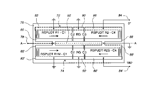
The balun resonator filter illustrated in Fig. 9 comprises two resonator filters 72
and 74 arranged side by side on a surface of a piezoelectric substrate 76. A center line
extending between the two resonator filters 72 and 74, parallel to the direction of surface
wave propagation, is denoted A-A for reference.
CA 0223383~ 1998-04-01
The resonator filter 72 is as described above with reference to Fig. 3, comprising
RSPUDTs Rl and R2, providing resonant cavities Cl and C4 respectively, and a central
reflection grating RG, with resonant cavities C2 and C3 between the reflection grating RG
and the RSPUDTs Rl and R2 respectively. A single-ended or unbalanced terminal 78 is
5 connected to a conductive rail 80 of the RSPUDT Rl, the other conductive rail 82 of
which is grounded. One terminal 84, referenced 0~, of a pair of balanced terminals 84,
84' is connected to a conductive rail 86 of the RSPUDT R2, the other conductive rail 88
of which is grounded. The reflection grating RG can be electrically floating, or grounded
via a conductive rail 90 as illustrated.
The resonator 74 is identical to the resonator filter 72 except for the phasing of its
RSPUDTs which are referenced RlM and R2S. Thus, using primed references
corresponding to those for the resonator filter 72, the unbalanced terminal 78 is also
connected to a conductive rail 80' of the RSPUDT RlM, the other conductive rail 82' of
which is grounded. The other terminal 84', referenced 180~, of the pair of balanced
terminals 84, 84' is connected to a conductive rail 86' of the RSPUDT R2S, the other
conductive rail 88' of which is grounded. The reflection grating RG can be electrically
floating, or grounded via a conductive rail 90' as illustrated. The same resonant cavities
Cl to C4 as for the resonator filter 72 are provided in the resonator filter 74 by the
RSPUDT RlM, between the reflection grating RG and the RSPUDTs RlM and R2S, and
by the RSPUDT R2S respectively.
The resonator filter 74 differs from the resonator filter 72 only in that the layout
and electrodes of the RSPUDT RlM are a mirror image, about the center line A-A, of the
layout and electrodes of the RSPUDT Rl, whereas the layout and electrodes of theRSPUDT R2S are the same as the layout and electrodes of the RSPUDT R2, i.e. they are
simply translated or shifted in the plane of the surface of the piezoelectric substrate 76.
Consequently, the path between the terminals 78 and 84' has a phase change of 180~
compared with the path between the terminals 78 and 84, whereby the terminals 84, 84'
provide a balanced termination (input or output) for the resonator filter, a good balance
being provided by the similarity of the resonator filters 72 and 74.
It is observed that the two resonator filters 72 and 74 can be close together with
only a small gap between them. Propagated surface waves are relatively well constrained
within the apertures of the filters because these are resonator filters, so that there is little or
no coupling of surface waves between the two resonator filters. In order to reduce any
coupling that may occur, the surface of the piezoelectric substrate 76 can be provided with
a groove along part or all of the length of the center line A-A between the resonator filters
72 and 74, as shown by a dashed line 92 in Fig. 9. Alternatively, the resonator filters 72
and 74 can be provided on separate, individual piezoelectric substrates which are mounted
in the same package.
CA 0223383~ 1998-04-01
In this respect it is also observed that the small width of each resonator filter and
their close spacing enables the balun resonator filter, having twice the width of a single
resonator filter, to be accommodated in the same size of package as a single unbalanced
resonator filter. For example, a balun resonator filter as illustrated in Fig. 9 for use at an
IF of about 200 MHz can be provided on a piezoelectric substrate 76 of the order of
12 mm long and 2 mm wide, each resonator filter (including the conductive rails) being of
the order of 0.7 mm wide, with a gap of the order of 0.2 mm between the resonator
filters. Such a balun resonator filter can be accommodated in the same size of package as
is used for a corresponding unbalanced resonator filter, for example as described with
10 reference to Fig. 3, which would require a piezoelectric substrate of the order of 12 mm
long and 1 mm wide.
It can be appreciated that Fig. 9 illustrates by way of example only one of
numerous alternative arrangements of balun resonator filter in accordance with this
invention. In particular, it is observed that each of the two resonator filters can have any
15 of the forms and alternatives described above with reference to Figs. 1 to 4, and can use
SPUDTs or RSPUDTs. Different connection arrangements can be provided for the twofilters, it only being necessary that the two resonator filters provide a phase difference of
180~ for the two signal paths between an unbalanced connection and a pair of balanced
connections. Thus, for example, instead of being as described above and illustrated in
20 Fig. 9, for the resonator filter 74 the RSPUDT R1 could be shifted and the RSPUDT R2
could be mirrored about the line A-A, and/or individual signal and ground connections to
the RSPUDTs could be interchanged. Alternatively, for the resonator filter 74 both of the
RSPUDTs R1 and R2 could be mirrored about the line A-A, or both could be shifted, and
the phase difference of 180~ could be provided by interch~nging connection wires to the
25 resonator filters. (For example, in Fig. 9 the mirrored RSPUDT RlM could instead be a
shifted version of the RSPUDT R1, with the upper rail 80' connected to ground and the
lower rail 82' connected to the terminal 78. The common bonding pad shown in Fig. 9
between the rails 80 and 80' would, of course, not be present in this case.) However, this
is not preferred, especially at high frequencies, because of the need for and imbalancing
30 effects of the connection wires.
It can also be appreciated that the invention is especially advantageous when
applied to RSPUDT and SPUDT resonator filters as described above because such
resonator filters can provide a desired filter order (e.g. a 4-pole filter) in a very narrow
structure, and providing two such structures side by side in the same package is very
35 practical. However, the principles of the invention can if desired also be applied to other
types of resonator filter, for example WCR and LCR filters as described in the
background of the invention. However, this is much less advantageous and practical
because a balun structure can be provided otherwise for such resonator filters, and their
CA 0223383~ 1998-04-01
widths (and hence package sizes) are much greater both by virtue of the structure of the
resonator filter itself and by a need to cascade two or more such filters to provide the
desired filter order, so that a further doubling to provide a balun function in accordance
with this invention is undesirable in practice.
Fig. 10 illustrates one alternative form of balun resonator filter, in which the two
resonator filters 94 and 96 each have the form described above with reference to Fig. 4,
providing three resonant cavities C1 to C3. In this balun resonator filter the balanced
terminals are connected to non-grounded inner conductive rails of RSPUDTs R1 and RlM
mirrored about the center line A-A, and the unbalanced terminal is connected to inner
10 conductive rails of RSPUDTs R2 and R2S, with the other, outer, conductive rails of all of
the RSPUDTs being grounded. As described above and shown by the dashed line 92, a
groove can be provided along part or all of the length of the center line A-A between the
resonator filters 94 and 96.
Although particular embodiments of the invention have been described in detail, it
15 should be appreciated that numerous modifications, variations, and adaptations may be
made within the scope of the invention as defined in the claims.