Note: Descriptions are shown in the official language in which they were submitted.
CA 02234770 1998-04-1~
W 097139422 PCT~US97/05426
PIPELINED PYRAMID PROCESSOR FOR
IMAGE PROCESSING SYST~MS
This non-provisional U.S. national application, filed under 35 U.S.C. 11 l(a) claims,
under 35 U.S.C. 119(e)(1), the benefit of the filing date of provisional U.S. application no.
60/015,276, filed under 35 U.S.C. 11 l(b) on April 17, 1996.
Field of the Invention
This invention relates to a method and apparatus of digitally processing image data and,
particularly, a method and appaldlus for performing image processing using pipelined image
processing operations combined together on a single integrated circuit.
Back~round of the Invention
Pipelined image processing operations involve the connection of discrete storage and
discrete pipelined image processing components which perform image operations. These
image processing operations include, for example, image convolution, image warping,
nonlinear image processing operations, and other specialized processes such as connected
component analysis of binary images. These systems do not integrate the processing and
storage circuitry into single devices. Typically, these components are connected together with
external crosspoint switches or dedicated data flow routing. The use of discrete image storage
and processing components results in large circuits that are difficult to fit on small printed
circuit boards. In addition, the use of discrete components and longer circuit paths reduces the
execution speeds of the processes.
Dedicated pipelined image processing components can provide very high performance
for image processing operations at a reduced cost to performance ratio over general-purpose
processors such as von Neumann and Harvard architectures. General-purpose processors
typically cannot provide fundamental image operations with the same performance as pipelined
architectures because general-purpose processors are ~imited to a data read-process-store
operation for each pixel operation.
Massively parallel processors and computers are typically very complex to program and
expensive to implement. In addition, the process of providing image data to each of the
processors in a timely manner before parallel execution begins is generally slow.
CA 02234770 1998-04-1~
W O 97139422 PCTrUS97/05426
Further, certain image processing operations are difficult to implement with parallel
architectures. While image convolution and other filtering operations that use re~atively small
pixel neighborhoods can be implemented efficiently in parallel systems, operations such as
image warping are still quite inefficient.
Summary of the Invention
The present invention is related to a pipelined parallel processor (PPP) integrated onto a
single integrated circuit. The PPP includes a filtering unit, internal routing circuitry such as a
crosspoint switch, an internal frame store controller, and one or more function circuits. The
function circuits may be, for example, arithmetic units, lookup tables, timing compensators,
10 adders/subtractors, statistics modules, image shifting circu;try, and other useful processing
devices. The components of the PPP are interconnected with the crosspoint switch which
routes data between the frame store controller, the filtering unit, function circuits, external
input channels, and external output channels.
Brief Description of the Drawin~
The invention is best understood from the following detailed description when read in
connection with the accompanying drawing, in which:
Fig. l is a block diagram of an exemplary embodiment of the present invention directed
to a pipelined parallel processor integrated on to a single integrated circuit.
Figs. 2(a)-2(d) are data structure diagrams of frarnes of an image signal illustrating the
2 o conceptual operation of an image stabilization process.
Fig. 3 is a flow chart diagram illustrating the image stabilization process of the frames
shown in Figs. 2(a)-2(d) in accordance with an exemplary embodiment of the present
invention.
Fig. 4 is data structure diagram illustrating the conceptual operation of the image
25 stabilization process shown in Fig. 3.
Fig. S is a block diagram of an exemplary embodiment of the present invention directed
to pipelined parallel processor integrated onto a single integrated circuit within an image
stabilization system.
CA 02234770 1998-04-1~
WO 97/39422 PCTAUS97/05426
Fig. 6 is a block diagram of the PPP 560 and memory 550 shown in Fig. S in
accordance with an exemplary embodiment of the present invention.
Fig. 7 is a timing diagram useful for explaining the operation of the PPP of Fig. 6.
Fig. 8 is a data flow diagram illustrating the operation of the image stabilization system
5 shown in Fig 6 in accordance with an exemplary embodiment of the present invention.
Fig. 9 is a block diagram of the frame store controllers 605 and 610 shown in Fig. 6 in
accordance with an exemplary embodiment of the present invention.
Figs. 10-12 are data structure diagrams illustrating the read region of interest RD_ROI
in memories 550a and 550b shown in Fig. 6.
Figs. 13-19 are timing diagrams useful for explaining the read operation of frame store
controller 605 and 610 shown in Fig. 6.
Figs. 20 and 21 are data structure diagrams illustrating the region of interest VVR_ROI
in memories 550a and 550b shown in Fig. 6.
Fig. 22 is timing diagram useful for explaining the write operation of frame store
controllers 605 and 610 shown in Fig. 6.
Fig. 23 is a block diagram of the interface circuitry 900 of the frame store controllers
605 and ~510 shown in Fig. 9 in accordance with an exemplary embodiment of the present
mventlon.
Fig. 24 is timing diagram useful for explaining the operation of interface circuitry
20 shown in Fig. 23.
Detailed Description of the Invention
Overview
The exemplary embodiment of the invention is directed to a Pipelined Pyramid
Processor (PPP) which integrates the most fundamental storage and processing aspects of the
25 front-end image processing operations into a single ASIC device. The fundamental storage and
processing aspects are implemented by a PPP having a filtering unit, internal routing circuitry,
an internal frame store controller, and one or more function circuits. Additional circuitry may
be added to the PPP to implement particular processing operations including arithmetic logic
CA 02234770 1998-04-1~
W 097/39422 PCTrU~97/05426
unit and digital signal procç~.~ing core operations. In addition, the components of the PPP may
be programmed to perform a variety of processing operations. In either case, the PPP provides
a flexible architecture that may be added to andlor programmed to perform a variety of image
processing operations. The PPP also provides an architecture from which ASICs may be
developed and produced. The filtering unit, internal routing circuitry, and internal frame store
controller provide a standardized architecture and interface for the addition and integration of
other components.
As a result, the amount of board space required to implement front-end image
processing systems is greatly reduce by integrating many components into a single device. In
o addition, the effective execution time of the image processing operations is decreased because
on-chip processing is typically performed at higher rates than processing that requires
communications among multiple discrete processing devices; in addition, these pipelined
operations may overlap. Finally, the processing systems can be implemented rapidly and with
minim~l integration because of the standardized architecture and interfaces.
Overview of First ExemplarY Implementation of PPP
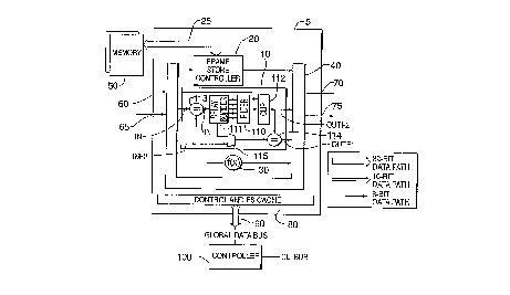
A first exemplary implementation of the PPP is described below with reference to Fig.
1. The PPP includes processing chcuiLI y which is implemented on a single integrated circuit
(IC) 5. The circuitry includes a filtering unit l 0, internal routing circuitry such as a crosspoint
switch 40, an internal frame store controller 20, and one or more function circuits 30. The
20 function circuits 30 can be arithmetic units, lookup tables, timing compensators,
adders/subtractors, statistics modules, image shifting circuitry, and other useful processing
devices. The devices are interconnected with the crosspoint switch 40 which routes image
information between the frame store controller 20, filtering unit lO, function circuits 30,
external input terminals 60 and 65, and external output terminals 70 and 75. The circuitry is
25 configured to accept input signals having imbedded timing signals. These timing signals arc
propagated through the circuitry with compensating delays to match the delays of the data
signals. These propagated timing signals are imbedded in the output signals.
The crosspoint switch 40 is a centralized non-blocking crosspoint switch. Crosspoint
switch 40 encodes channels of image data along with timing information to enable multiple
3 o channels of image information to be processed without interference. Crosspoint switch 40 is
CA 02234770 1998-04-1~
W O 97/39422 PCT~US97/05426
used to route image data between frame store controller 20, filtering unit l0, function circuits
30, input channels 60 and 65 and output channels 70 and 75.
The input data signals and the output data signals of frame store controller 20 are
connected directly to crosspoint switch 40 which routes the image data between frame store
controller 20 and the other circuitry connected to crosspoint switch 40. The frame store
controller resamples image data signals during image read and store operations and executes
read and store operations simultaneously. The frame store controller 20 may also include an
access port ~not shown) to allow the frame store controller 20 to be accessed through a global
data bus 90 for processor read and store operations without passing through crosspoint switch
40-
Filter unit l0 may be a two-dimensional filter having a separable kernel which can be
treated as a combination of separate horizontal and vertical filters. The five vertical and five
horizontal filter coefficients of the exemplary filter unit l0 are programmable within a limited
set of values a,nd may be either symmetric or antisymmetric. In addition, the filter unit l 0 may
be configured to have either an odd or an even number of taps. The filter unit l0 combined
with the frame store controller 20 can be used for many types of image filtering applications.
These include the efficient generation of multiresolution representations of imagery (i.e. image
pyramids) as described in U.S. Patent No. 5,359,674, entitled PYRAMID PROC~SSOR
INTEGRATED CIRCUIT, issued to van der Wal, which is incorporation herein by reference.
Multiresolution (pyramid) representations in image processing are used for efficient image
processing operations including, for example, image feature analysis, image compression,
image registration (alignment), and motion estimation. These applications use the resampling
operation of frame store controller 20, described below, for image decimation and expansion
operations that are a part of pyramid generation and reconstruction.
Function circuits 30 may implement a variety of different image processing functions.
These functions include (l) fundamental arithmetic operations at differing levels of precision,
(2) albi~ y pointwise single image operations, (3) arbitrary pointwise dual image operations,
(4) image statistical analysis, and (5) nonlinear image filtering. These functions are described
below.
CA 02234770 1998-04-1~
WO 97/39422 PCT~US97/05426
Fundamental arithmetic operations are used in many image operations. These include
the detection of image intensity changes and image motion estimation, which use image
addition, subtraction, multiplication, and division.
Arbitrary pointwise single image operations are used to process image data. Both linear
5 and nonlinear functions of pixel values may be used during image processing to provide useful
processing results. These operations include adding gain to images, implementing image
thresholding operations, and inverting images. A programmable look-up table is typically used
to implement these operations in a flexible manner.
Many operations in front-end processing use arbitrary pointwise operations on two
images. The arbitrary pointwise operations include image m~sking, image modulo arithmetic,
i.e. one image modulo with another image, and other image operations where the resulting
image is the same precision as either of the input images. Operations such as image
multiplication, sum-squared, and sum-absolute difference, may also be implemented using
arbitrary pointwise operations if the output is scaled to retain the same precision as the inputs.
Usually, a programmable look-up table is used to implement these operations if a large amount
of memory is available internal or external to the chip (e.g. 64k x 8). Alternatively, many of
the functions can be implemented directly in the PPP.
Image statistical analysis such as the generation of image histograms and accumulation
over the entire image or subregion of the image are used to accuratcly determine ~ uL~iate
thresholds, to determine the amount of image energy in a given scene, and to interprct cross-
correlation surfaces and other obJective functions for motion estimation and image alignment.
Nonlinear image filtering is used to perform spatial operations such as minimllm,
maximum, and median filtering which are very important for cleaning up and conditioning
processed image data for further processing. These operations are typically very cxpensive to
implement using general-purpose processors, but are readily available using the PPP. One such
device whose functional circuits may be incorporated into the PPP is Median/Max/Min Filter
part no. IP90c20 manufactured by Sumitomo Metals.
The PPP incorporates a subset of these operations into a single integrated circuit with
an internal crosspoint switch 40 for flexible on-chip routing of the video information through
3 o the various processing devices. This provides very efficient Implementations of many front-
CA 02234770 1998-04-1~
W 097/39422 PCT~US97/05426
end processes, while integrating the components so they can be efficiently incorporated into
final proces~ing architectures and devices with a minim:~l amount of circuit board space and
cost. The performance of the PPP in implementing any of these functions will typically be an
order of magnitude or more better than the same processing being performed with general-
purpose processors, and typically be a fraction of the cost of massively parallel processing
systems.
The function circuitry 30 may be, for example, a look-up table (LUT) having a
programmable registered memory capable of performing arbitrary pointwise operations on a
single image. The LUT can be used for increasing gain of image data, applying nonlinearities
to the image data, inverting the image data, and other single image operations. The functions
of the LUT is programmed through global bus 90. Different functions of the ~UT may be
stored in the PPP to reduce setup time when programming the LUT.
Using 0.5,u or the current state of the art 0.35,u CMOS designs, the minim:~l
implementation PPP may be incorporated into a single ASIC. Such an ASIC would be capable
of running at internal speeds of 60 Mhz or higher. Using 0.35~ CMOS designs will not only
reduce the die size of the PPP, but will increase the processing speeds and reduce the power
dissipation of the PPP.
The operation of the different components shown in Fig. l will be described in greater
detail using an exemplary application of the PPP to perform image stabilization. Although the
exemplary embodiment of the present invention is explained below with reference to a specific
image processing application, the PPP is applicable to many different image processing
applications.
Detailed Description Of The Exemplary Application
Overview of Ima~e Stabilization
2 5 Video captured by a hand held camera, or by a tripod-mounted camera with a large
telephoto lens often exhibits some random image motion. Reducing thc image motion is very
desirable for viewing such video. Image stabilization is a process which elimin~tes or reduces
a component of the image motion in a video sequence. Accurate image stabilization can
greatly enhance the ability to analyze or further process video by means of a digital processor
3 o and, therefore, considered a very important "vision-front-end" image process. Image
CA 02234770 1998-04-1~
W 097/39422 rCT~US97/05426
stabilization can be applied in several modes. One mode removes all image motion, which
makes it appear as if the video camera was completely stationary. Another form of
stabilization smoothes the image motion, by e]imin~ting only fast image motion, but allowing
for slow image motion, such as image panning, to occur.
Image stabilization can be achieved by determining the image motion between
consecutive image frames, and then compensating for this image motion by warping, i.e. -
~ligning, the current frame towards a previous frame so that its image aligns with the image of
that previous frame. An example of several consecutive frames of an video image signal is
shown in Figure 2(a) where t indicates an instant in time. The video image signal includes a
sequence of four video frames F(t), F(t+l), F(t+2), and F(t+3), where there is an apparent
random motion of the image 200 in the four frames.
Fig. 2(b) shows the four frames F(t), F(t+l), F(t+2), and F(t+3) superimposed toillustrate the amount of image motion among the four frames. Fig. 2(c) illustrates the four
frames F(t), F(t~l), F(t+2), and F(t+3) after image stabilization according to the first method.
The subsequent image frames F(t+l), F(t+2), and F(t+3) are aligned to the frame F(t). Fig. 2(d)
illustrates the four frames F(t), F(t+l), F(t+2), and F(t+3) after image stabilization according to
a second method where image stabilization is implemented by "smoothing" thc image motion.
There is a general motion of the image to the right in Fig. 2(d).
Fig. 3 is a flow chart illustrating the stabilization method for stabilizing a video image
signal. At step 300, the method determines the image motion between the current frame F(t)
and a previous frame F(t- l ) . Then, at step 3 l 0, the alignment parameters Cz are generated to
align the current image F(t) to the reference frame, or to an image position at which unwanted
image motion is removed. At step 320, the current image is re-aligned, i.e. - warped, according
to the alignment parameters Cz. The stabilization method of Fig. 3 is illustrated in Fig. 4.
As shown in Fig. 4, a set of image correlations are performed in a hierarchical fashion
to determine the amount of image motion that has occurred between the current frame F(t) and
the previous frame F(t- l ). To determine the amount of image motion, an image pyramid is
generated from the current frame F(t). For example, the Laplacian pyramid Lz(t-l) to Lz(t-l),
for example Lo(t- l ) to L4(t- l ), is generated for the previous frame F(t- l ) and the Laplacian
3 o pyramid Lz(t) to Lz(t), for example Lo(t) to L4(x), is generated for the current frame F(t). The
CA 02234770 l998-04-l~
WO 97/39422 PCT~US97/05426
correlation between the current frame F(t) and the previous frame F(t- 1 ) are performed using a
sixty four pixel value by sixty four pixel value region of the frames.
For each level, the correlation values Cz(i,j) are generated in accordance with e~uation
(I) below.
Cn(i~ n(x + i~ y ~ j~ t).L"(x, y, t--I)
x ~ ~--(1)
where x and y are coordinates of the pixels values in the nth level of the Laplacian image
pyramid and i and j are integers and -2 ~ i < 2 and -2 ~ j ~ 2. For example, when there are four
levels of the Laplacian pyramid, z = 1, 2, 3, or 4. Twenty five correlation values Cz(i,j) may be
produced at pyramid level z = 4 because pyramid level four includes sixteen pixel values
10 corresponding to the pixels of the framcs. In other words, a five pixel value by five pixel value
region correlation at level four represents a total correlation search space of 64-by-64 pixel
values in each of the current frame F(t) and the previous frame F(t- 1).
A simple maximum search is performed on the twenty five correlation values Cz(i,j) to
determine the location of the maximum correlation value Cz(i,j)max. Once the maximum
15 correlation value has been determined, the correlation values Cz(i,j) adjacent to and including
the maximum correlation value Cz(i,j)max are interpolated to estimate the maximum peak
correlation value Cz(i,j)peak of the correlation values Cz(i,j) to sub-pixel accuracy. The peak
correlation value Cz(i,j)peak provides an estimate of the image motion, relative to the image
resolution of the pyramid level at which the correlation values Cz(i,j) are generated. At level z
20 = 4, the estimate is coarse but motions are stim~ ted over a large range.
Next, the peak correlation value Cz(i,j)peak for the next higher resolution level z = 3 is
produced. Prior to gencrating correlation values between previous Laplacian image Lz(t-1) and
the current Laplacian image Lz(t), the prcvious Laplacian image Lz(t-1) is first warped with the
course motion estimate, peak correlation value C4(i,j)peak, obtained from the correlation at
- 25 level four, z = 4. Thus, the correlation computation at level three, z = 3, is a refinement of the
previous motion estimate. At level three, the expected residual motion is less than l 1 pixel
value per line. A three-by-three value region in the Laplacian image at level three, z = 3, is
used to generate the correlation values C3(i,j).
CA 02234770 1998-04-1~
W O 97/39422 PCT~US97/05426
The image motion estimate is refined again by repeating this process at level 2.Typically, the motion estimate obtained at this resolution is better than one tenth the pixel
resolution of level zero, z = 0, if the image motion was a pure translation. The peak correlation
values Cz(i,j)peak are added and used to warp the current frame F(T) and stabilize the image.
Detailed description of the Ima~:e Stabilization Svstem
The image stabilization system is described below with reference to Figs. 5-7. Fig. 5 is
a block diagram of the image stabilization system according to an exemplary embodiment of
the present invention. A color video signal is provided to input terminal IN of the video
stabilization system 500. The color video signal is an NTSC video signal digitized to
0 component digital image format 4:2:2. Alternatively, the color video signal may be a standard
component digital format such as CCIR601, D1 format. The D1 format has 1440 pixels per
line, where the luminance component signal Y has 720 pixel values and the chrominance
component signal has two chrominance component signals each including 320 pixelsinterleaved into a single data stream. Another possible input may be an MPEG encoded signal
that is decoded into linear scan image format.
The color video signal is provided to input video decoder 510 which is, for example, a
Philips Part No. SAA7110. The input video decoder 510 digitizes the color video signal and
generates two digital video output signal streams: the luminance component signal Y and the
chrominance component signals Cu and Cv, in 4:2:2 format. The lllmin~nc.e component signal
Y is represented at full digitized resolution, i.e. - 640 active pixel values per line, and the
chrominance component signals Cv and Cu are subsampled at a factor of two in the horizontal
direction, i.e. - 320 active pixel values per line. The chrominance component signals Cv and
Cu are interleaved to form 640 pixel values per line. Alternatively, the video decoder could bc
integrated in the PPP 560.
Table I below illustrates the two data streams, where Cu and Cv are the two color
components, Y is the luminance component, and the index is the pixel value number on thc
image line.
TABLE 1
Luminance Signal Y0 Y1 Y2 Y3 Y4 Y5 Y6 Y7 Y8
Chrorninance Signal CuO CvO Cu2 Cv2 Cu4 Cv4
CA 02234770 1998-04-1~
W O 97/3942Z PCTrUS97105426
The luminance component signal Y is provided to frame buffer 530 and the
chromin:lnce component signal is provided to frame buffer 520. The ll-min,.nce and
chrominance component signals are provided to these respective frame buffers at a clock rate at
12.5 MHz to 13.5 MHz. Each frame buffer 520 and 530 is double buffered so that luminance
component signal Y and the interleaved chrominance component signals Cu and Cv may be
stored in one buffer at a clock rate of 13.5 MHz and read from the other buffer at a clock rate of
60 MHz. An example of frame buffers 520 and 530 is Hitachi part no. HM530281, which can
store 332k pixel values of data.
The luminance component signal Y and the chrominance component signals Cu and Cvare provided to Pipelined Parallel Processor (PPP) 560 which is a single integrated circuit.
PPP 560 implements the stabilization process described above. PPP 560 is described below
with reference to Fig. 6. PPP 560 includes crosspoint switch circuitry 640, filter units 615 and
620, two delays 625a and 625b coupled respcctively to multipliers 630a and 630b which are in
turn respectively coupled to accumulators 635a and 635b, two frame store controllers 605 and
610 which are respectively coupled to memories 550a and 550b which form memory 550,
shown in Fig. S, and look-up table (LUT) 645.
The crosspoint switch 640 may be the same as crosspoint switch 40, shown in Fig. 1.
Crosspoint switch 640 is provided the luminance component signal Y via terminal IN1 and the
chro",ill~nce component signals via terminal IN2. The luminance and chrominance component
signals are multibit digital signals containing at least cight data bits and two timing bits. The
two timing bits convey respective timing signals. One signal, HA, is in a logic high state when
the data in a line is valid (i.e. during the active picture interval) and in a logic low state
otherwise (i.e. during the horizontal blanking interval). The other signal, VA, is in a logic high
state when the data in a frame is valid and in a logic low state otherwise (i.e. during the vertical
blanking interval). Figure 7 is a timing diagram which illustrates the relative timing of the
signal provided to terminal INI and the signal provided from output terminal OUT1, and the
signals HA and VA for those signals. The exemplary operation shown in this timing diagram
delays the output signal by approximately two line intervals with respect to the input signal.
The PPP 560 uses the timing signals HA and VA in the same manner as described inthe above-referenced U.S. Patent No. 5,359,674. The timing signals HA and VA remain
associated with the input image signal as the input image signal is processed by the
11
CA 02234770 1998-04-1~
W097/39422 PCTAUS97/OS426
stabi}ization system 500. As a result, when the stabilized image signal is produced, the vertical
and horizontal blanking periods of the stabilized image signal do not need to be generated. The
relative timing of the stabilized image signal is m~in~zlined by associating the timing signals
HA and VA with the color video signal as it is processed. Thus, less circuitry is required.
The two delays 625a and 6~5b may serve several functions. The delays 625a and 625b
provide a programmed delay operation to delay one digital image data stream relative to
another digital image data stream to compute cross correlation or other two-operand functions
that require a shift location in the horizontal or vertical direction between two images. The
delays 61 Sa and 61 Sb also provide automatic alignment in time of two image data streams. For
examplc, the delays 615a and 615b align two image data streams in time if the two image data
streams are to be combined in a two-operand function using, for example, multiplier 630a. The
two image data streams may not be aligned in time because they have encountered different
delays through the device. For example, the image data streams may not be aligned if one
image data stream is passed through LUT 645 and the other image data strcam is not. The
image data timing signals HA and VA associated with each image data stream allow the delays
615a and 615b to automatically detect the time difference between the two image data streams
and delay one image data stream such that the two image data streams are aligned in time when
presented to the two-operand function. The programmed delay operation may be combined
with the automatic alignment operation.
The exemplary embodiment is not limited to processing multibit digital signals
containing eight data bits and two timing bits. The exemplary embodiment may be configured
to receive multibit digital signals containing, for example, 10 data bits and two timing bits.
l~eferring to Fig. 6, crosspoint switch 640 enables signals provided via input terminals
~1 and IN2 to be connected to any of the output terminals OUTI and OUT2, withoutinterfering or blocking any of the other channels within the crosspoint switch 640 for
maximum parallelism and interconnectivity. The routing performed by the crosspoint switch
640 is programmable from an external controller 595, shown in Fig. 5, through global data bus
645. Exemplary circuitry which can be used for crosspoint switch 640 and externa] controllcr
595 is the LSI Logic crosspoint switch part number L64270 QC~0.
CA 02234770 1998-04-1=,
W O 97/39422 PCTrUS97/05426
Fig. 8 is data flow diagram suitable for illustrating the operation of the videostabilization system 500 and, particularly, the PPP 560, shown in Fig. 5. In general, as is
- shown in Fig. 8, a number of different processes are implemented by the PPP 560 during one
cycle to stabilize the image.
In process block 810, a Gaussian image Gl(t)Y is generated from a lllmin~nce
component signal Y provided to the PPP 560 from frame buffer 530, shown in Fig. 5. In
process block 815, the Gaussian image Gl(t)Y is used to produce lower level Gaussian images
Gn+l(t) and the Laplacian image pyramid, shown in Fig. 4. Each time process block 815 is
repeated, one of the Laplacian images LO(t) through L4(t), shown in Fig. 4, is produced.
Although process block 815 is repeated, the time required to produce the Laplacian image
pyramid and the lower level Gaussian images is less than the amount of time required to
produce the Gaussian image Gl(t)Y in process block 810. This occurs bccause the number of
pixel values in the Laplacian and ~ n images are reduccd by, for example, one fourth for
each level of the Gaussian and Laplacian images. Thus, there are fewer pixel values to be
processed by process block 815.
In process block 820, after the Laplacian pyramid has been produced, the Laplacian
images LO(t) through L4(t) and the Laplacian images LO(t-l) through L4(t-1) produced during a
previous cycle, are used to generate the alignment parameters C(x, y) as described above with
reference to Fig. 4. In process block 825 during the next cycle, the alignment parameters C(x,
y) are used to warp the luminance component signal Y of the input image frame (IIF) from the
prcvious cycle. In process block 830, the ~lignment parameters C(x, y) are used to warp the
chrominance component signals Cu and Cv of the IIF from the previous cycle. In process
block 835, the chromin~nce component signal of the next frame is provided to the PPP 560,
shown in Fig. 5, frame buffer 520. Process blocks 810 through 835 align the frames of an input
image signal. The stabilization process is described in greater detail below.
The stabilization process performed by PPP is divided into three steps, where each step
consists of two or more parallel processes. The steps are~ enerate first Gaussian level,
- section 800a, (2) gcnerate Laplacian pyramid, section 800b, and (3) perform hierarchical image
correlations, section 800c. The total time required for the PPP 560 to complete all three steps
iS about 14 msec assuming a 50 Mhz clock. The stabilization process is performed by the PPP
560, and consists of a set of operations performed in parallel and in series, all within one field
~3
CA 02234770 1998-04-1~
W 097/39422 PCT~US97/05426
time. If the video format is a 30 Hz video format (e.g NTSC), the field time is about 16.7
msec.
As is shown in Figs. 6 and 8, the luminance component signal Y is provided from
buffer 530, shown in Fig. 5, to crosspoint switch 640, shown in Fig. 6, which routes the
lllmin:lnce component signal Y to frame store controller 610 and filter unit 615. Filter unit 615
is a pyramid filter unit and is the same as the filter unit 10, shown in Fig. 1. As is shown in
Fig. 1, line delay and border control (hereinafter delay\border control~ circuitry 111 provides a
four or eight-line delay for the vertical portion of the two-dimensional filter. The delayed lines
are processed both vertically and horizontally in delay\border control circuitry 111. Filter
Cil~;ui~ 110 and line delays and border control circuitry 111 are, for example, the filter 110,
memory 1 14, address counter 116, and timing circuitry 12~, described in the above referenced
patent issued to van der Wal.
The delay/border control circuitry 111 ensures that border effects are minimi7Pd in the
filter unit 615 by edge extending, lllhl~3lhlg, or blanking out the pixel values outside of the
region of the image before filtering. The delay/border control circuitry 111 can also be used to
provide spread-tap (resampled) filtering, and can be used to zero out intermediate pixels in the
image for accurate image interpolation operations.
The output signal provided by filter circuitry 110 is processed by clip processing
circuitry 1 12 which performs rounding and scaling for single precision signals and combines
2c the filtered data as the more significant bit (MSB) positions with filtered data representing the
less significant bit ~LSB) positions to generate double-precision output signals. Clip
processing circuitry 112 corresponds to, for example, clip proccssing ch~;uiLr,y 124 described in
the above-referenced U.S. Patent No. 5,359,674.
The signal provided by multiplexer circuitry 1 15 may be either the input signal INF2 or
one of the delayed horizontal line signals provided by the delay/border control 111.
Multiplexer circuitry 115 is coupled to internal compensating delays (not shown) in the
delay/border control 111. The internal compensating delays are used to delay the input signal
INF1 from one to eight lines intervals. Multiplexing circuitry 115 selects among the input
signal INF1 delayed by one to eight line intervals or input signal INF2.
14
CA 02234770 1998-04-1~
W O 97/39422 PCT~US97/05426
The output signal of multiplexer 115 and clip processing circuitry 112 can be processed
by ALU 114 to produce output signal OUTFI. ALU 114 operates the same as ALU 113 of the
- above referenced patent issued to van der Wal. ALU 114 is used to perform operations
between the filtered image and the nonfiltered image, or can pass one of the images without
modification. Filter unit 615 has two parallel paths which may be used to simultaneously
calculate a Gaussian low-pass filtered image and a Laplacian function (the difference of the
input image and the CT~ S;~n) of the input image. As is shown in Fig. 1, the Laplacian image
may be generated by the ALU 114 which receives the Gaussian image from clip circuitry 112
and a delayed input image from delay/border control 111 and multiple~cer 115. The Gaussian
and Laplacian images are used during image stabilization as described below. The generation
of Gaussian and Laplacian images using filter unit 615 is described in the above referenced
patent issued to van der Wal.
Returning to Fig. 8, section 800a, the luminance component signal is provided to filter
unit 615 which generates a G~ .ci~n image signal Gl(t)Y of the luminance component signal
which is provided via crosspoint switch circuitry 640 to frame store controller 605. The frame
store controller 605 subsamples and stores the Gaussian image signal Gl(t)Y in memory 550a.
The subsampling and storing operations of the frame store controller 605 are described below.
The input luminance component signal Y (hereinafter G~lcsi:~n image signal GO(t)Y~ is
provided to frame store controller 610 which stores the Gaussian image signal GO(t)Y. Frame
store controllers 605 and 610 operate in the same manner and are described below after the
description of the operation of the stabilization system 500. In parallel, the luminance
component of the previous image aO(t-l)Y stored in memory 550b is retrieved using frame
store controller 610 which generates an interm~di:~te warped image. The intermediate warped
image is further warped using filter unit 620. Filter unit 620 may be a separable five by five
filter which includes 10 multipliers.
The previous image GO(t-l)Y is warped using alignment parameters C(i,j) produced in
the previous frame interval by section 800c, shown in Fig. 8. The peak alignment parameters
C(i,j)peak from the previous frame interval are provided to microprocessor 540. As is
described below, process block 820 is repeated to produce the peak alignment parameters
C(i,j)peak between the Laplacian images Ln(t-l) and Ln(t). The peak alignment parameters
C(i,j)peak for each level further refine the warping process to stabilize the image.
CA 02234770 1998-04-1~
W O 97/39422 PCTrUS97/05426
Microprocessor 5~0 accnm~ tes the peak alignment parameters C(i,j)peak generated for each
level of the Laplacian pyramid from the most significant bit position to the less significant bit
position. In other words, microprocessor 540 produces an accnm~ terl peak alignment
parameter C~i,j)peak from the alignment parameters produced at each level of the Laplacian
5 pyramid. Microprocessor 540 uses the accllmlll:-ted :ll;gnm~nt parameter to program filter unit
620 and frame store controller 610 to warp the luminance component signal of the input image
G0(t-l)Y as described below.
The generation of the ~lignmt~nt parameters is described below. The alignment
parameters include an integer value and a fractional value. An intermediate warped image can
10 be generated using the integer part C(xi, yi) of the ~lignment parameters C(x, y). The integer
part C(xi, yi) of the alignment parameters C(i,j) includes a horizontal component xi and a
vertical component yi which specify a translation of the previous image G0(t-l)Y in the
horizontal and vertical directions, respectively. The frame store controller 610 retrieves pixel
values from memory 550b which are included in a region of interest RD_ROI, shown in Figs.
10-11, and described below. The region of interest RD_ROI is a rectangular region in memory
550b, shown in Fig. 6. When pixel values are retrieved from memory 550b using frame store
controller 610, shown in Fig. 6, the size and starting coordinates of the read region of interest
RD_ROI in memory 550b are specified.
Framc store controller 605 warps the previous image G0(t-1)Y by shifting the read
20 region of interest RD_ROI, shown in Fig. 10, in response to the horizontal component xi and
vertical component yi of the integer part of the ~lignment parameters C(i,j). For example,
assume the region of intercst RD_ROI to be retrieved from memory 550b has starting
coordinate values (RD_HZERO= 2, RD_VZERO = 8) where data value RD_HZERO, shown
in Fig. 10, is the horizontal starting coordinate of the read region of interest RD_ROI and data
25 value RD_VZERO, shown in Fig. 10, is the vertical starting coordinate of the read region of
interest RD_ROI. If the horizontal component xi is four and the vertical component yi is five,
the starting coordinates are adjusted to (RD_HZERO = 6, RD_VZ~RO = 13). As a result,
image data which is retrieved from memory 550b by frame store controller 610 is warped by
the integer part of the ~lignment values C(i,j).
3 0 Next, filter unit 620, interpolates the interm~ e warped image using the fractional
part of the peak alignment parameter C(i,j)peak to complete the warping of the image.
16
CA 02234770 1998-04-1~
W O 97/39422 PCT~US97/05426
Microprocessor 540, shown in Fig. 5, uses the peak alignment parameter C(i,j)peak to program
the filter unit 620, shown in Fig. 6, to warp the hlmin:lnc~e component of the image. The peak
- alignment parameter C(i,j)peak specifies the degree to which the image is warped.
Each of the pixe] values in the image are warped by the peak alignment parameter5 C(i,j)peak to align the images in the frames as is shown in Figs. 2(a)-2(d). Thus, it is desirable
to warp each pixel value in the frame using the same fractional translation. Therefore, filter
unit 620 may be programmed to implement a two-by-two bilinear interpolation operation.
Alternatively, filter unit 620 may be a two-by-two separable filter. One such bilinear
interpolation filter is TRW part number TMC2301 described in Real-time Bilinear
10 Interpolation Using the TMC2241 by Steve Gomez, TRW LSI Products Division, and dated
January 21, 1989, which is incorporated herein by reference for its teachings on bilinear
interpolation.
For example, if the fractional part C(xf, yf) of the alignment values is 0.3 pixel values
in the horizontal direction, and 0.4 pixel values in the vertical direction, then a two tap
horizontal filter with coefficient values 0.7 and 0.3, and a two tap vertical filter with
coefficients 0.6 and 0.4 are used to implement the bilinear interpolation. The filter unit 620
may also implement higher order interpolation operations to increase the quality of the image
interpolation.
Returning to Fig. 8. once section 800a is complete, the steps shown in section 800b arc
20 performed. The Gaussian image Gn(t)Y is retrieved from memory 550a using frame store
controller 605. The Gaussian image Gn(t)Y is filtered using filter unit 615 to produce the next
level Gaussian image Gn+l(t)Y. For example, if Gaussian image Gl(t)Y is retrieved from
frame store controller 605, filter unit 615 produces Gaussian image G2(t)Y. Filter unit 615
performs the same operations as describcd above with reference to section 800a and Gaussian
25 image Gl(t)Y. Gaussian image Gn+l (t)Y is then storcd in memory 550a using frame store
controller 605. Framc store controller 605 subsamples the Gaussian image Gn+1 (t)Y prior to
storage of the Gaussian image in memory 550a.
Filter unit 615 also subtracts the Gaussian image Gn+l(t)Y from Gaussian image
Gn(t)Y to produce Laplacian image Ln(t). Laplacian image Ln(t) is then processed using LUT
645 which is used to enhance the Laplacian image Ln(t) to produce image Ln(t)' . LUT 645 is
CA 02234770 1998-04-1~
W 097/39422 PCT~US97/0~426
an eight bit LUT. The enhanced Laplacian image Ln(t)' is then stored in memory 550b using
frame store controller 610.
The above steps of section 800b are repeated for n e~uals 2, 3, and 4 to generate
Laplacian images Ll(t) through L4(t) and C~ c~i~n images G2(t) through G4(t). As each
5 successive image contains one fourth of the number of pixels as the previous image, the
processing time to repeat the steps of section 800b is approximately the same as the processing
time for generating ~T~ussi~n image G0(t) in section 800a. Laplacian images Ll(t) through
L4(t) are each stored in memory 550b using frame store controller 610. The above steps for
generating (~llc.ci:~n image Gn+l(t) and Laplacian images Ll(t) through L4(t) are completed in
10 about 3.2 msec.
In parallel with the steps described above in section 800b, the chrominance component
of the previous ( .allc~i~n image G0(t- l )C is retrieved from memory 550b and warped using
frame store controller 610 and filter unit 620. Frame store controller 605 and 610 operate in
the same manner to warp the chrominance component as described above to warp theluminance component. The warping of one field or half a frame of the previous color image
data is completed in about 3.7 msec. Once the color component of the previous Gaussian
image G0(t-l)C is warped, it is stored in frame buffer 570. The warped color component is
provided to frame buffer 570 via crosspoint switch 640, shown in Fig. 6, through output
terrninal OUTI.
As described above, the stabilization process first performs image correlations over a
five-by-five region of Laplacian image LA to produce alignment parameters C4(i,j). l'he
maximum alignment parameter C4(i,j)max is then selected from the alignment parameters
C4(i,j). Finally, the peak alignment parameter C4(i,j)peak is produced. The peak alignment
parameter C4(iJ)peak is then used to warp Laplacian image L3. In the same manner as for
level four, the pcak alignment parameter C3(i,j~peak is produced for level three. The peak
alignment parameter C3(i,j)peak is used to warp the Laplacian image L2. In the same manner
as for level three, the peak alignment parameter C2(i,j)peak is produced for level two. Section
800c shown of Fig. 8 illustrates how these operations are implemented in the PPP 560.
Laplacian image L4(t- 1) is retrieved from frame store controller 610 and provided to
filter unit 620. Laplacian image L4(t-1) is passed through filter unit 620 and provided to delays
18
CA 02234770 1998-04-1~
W O 97/39422 PCTAUS97/0542G
625a and 625b. In other words, Laplacian image L4(t-1) is not warped. The Laplacian image
L4(t) is retrieved from memory 550b using frame store controller 610 and provided to delays
~ 625a and 625b. The retrieval of Laplacian image L4(t) is delayed to compensate for the time
delay incurred when Laplacian image 1_4(t- 1) is passed through filter unit 620.
As described above, the first image to be warped in the Laplacian pyramid is Laplacian
image L3(t-1) using alignment parameters C4(i,j). If Laplacian image L4(t-1) is provided to
filter unit 620, filter unit 620 passes the Laplacian image L4(t-1) to delays 625a and 625b
without warping.
Delays 625a and 625b, multipliers 630a and 630b, accumulators 635a and 635b are
lo used to implement e~uation (3) above where n equals 4 (n = 4). Delays 625a and 625b are at
least four pixel value delays long so that the ~lopliate pixels values in thc Laplacians images
L4(t-1) and L4(t) may be multiplied using multipliers 635a and 635b and subsequently
accumulated using accumulators 635a and 635b to generate alignment parameters C4(i,j). The
alignment parameters C4(i,j) are provided to statistical unit 647, shown in Figure 6, which
determines the maximum alignment parameter C4(i,j)max. Then, the ~lignment parameters
C4(i,j) adjacent to the maximum alignment parameter C4(i,j)max are provided to filter unit
620. Filter unit 620 uses a two-by-two neighborhood of alignment parameters C4(i,j) including
the maximum alignment parameter C4(i,j)max to generate the peak alignment parameter.
Filter unit 620 implements a bilinear interpolation to generate the peak alignment parameter
C4(i,j) peak from the two-by-two pixel neighborhood.
The peak alignment parameter C4(i,j) is provided to processor 540. Generation of the
peak alignment parameter Cn(i,j) includes three iterations of the steps described above in
section 800c. The time to complete these steps is about 6.6 msec. After each iteration,
microprocessor 540 accumulates the peak alignment parameters C4(i,j)peak, C3,(i,j)peak, and
C2(i,j) for cach level of the Laplacian pyramid from the most significant bit position to the less
significant bit position. Microprocessor 540 uses the accum~ t~l alignment parameter to
program filter unit 620 and frame store controllers 605 and 610 to warp the images.
The same steps described above are used to generate the alignment parameters Cn(i,j)
for level three (n=3) and two (n=2) except that the previous image is warped using the
accumulated peak alignment parameter. For example, Laplacian image L3(t-1) is warped by
19
CA 02234770 1998-04-1~
W O 97/39422 PCTrUS97/05426
filter 620 in response to the acc~ t~d peak alignment parameter which is peak alignment
parameter C4(iJ) for level 4. Laplacian image L2(t-1) is warped by filter 620 in response to the
accllmlll~te~l peak alignment parameter which is an accumulation of peak ~lignm~nt parameter
C4(i,j) for level 4 and peak alignment parameter C3(i,j) for level 3.
In parallel with the steps described above in section 800c, the current chromin~nce
component of the current image G0(t) is provide to frame store controller 605 and stored in
memory 550a via crosspoint switch 620, shown in Fig. 6. Transfer and storage of the
chromin~nce component is about 3.7 msec. Pixel values are stored in frame buffers 570 and
580 at a clock rate of 50 MHz, while data is retrieved from the frame buffers 570 and 580 by
the video output encoder 590 at substantially the same time at a clock rate of 12.5 to 13.5 MHz,
which requires about 16 msec to read the data stored in the buffers. The frame buffers 570 and
580 are double buffered.
Returning to Fig. 5, the stabilized luminance component signal Y and the stabilized
chrominance component signals Cv and Cu are respectively provided from frame buffers 580
and 570 to encoder 590. Encoder 590 combines the components to produce a color video
signal at output terminal OUT. The encoder 590 is, for example, a Philips part number
SAA7187 device.
In Fig. 5, microprocessor 540 is used to program the encoder 590 and dccoder 510, and
to control the image processing functions of the PPP 560, via processor signal PS.
Microprocessor 540 is also used to program registers in the frame store controllers 605 and 610
for each of the steps of the stabilization process described above. Microprocessor 540 should
operate at a rate of, for example, 20 MHz, so that reprogramming time between each
processing step of the stabilization process is minimi7~d. Microprocessor 540 has a program
memory for storing code to operate the stabilization system 500. Microprocessor 540 may also
2~ include connections to an external EPROM, e.g. - a FLASH EPROM (not shown), for boot-up
procedures for the stabilization system. In an alternative embodiment, microprocessor 540 may
be incorporated into PPP 560. This may reduce the manufacturing cost of such a system.
Control circuitry 595 controls the interface between input and output buses of decoder
510 and encoder 590, and the interface and counters (not shown) to control frame buffers 520,
530, 570, and 580. Control cil~;uilry 595 also extracts the timing signal HA and signal VA
CA 02234770 1998-04-1~
W O 97139422 PCT~US97/05426
which are used to control the operation between buffers 520 and 530 and PPP 560, and
between the buffers 570 and 580 and encoder S90. Control circuitry 595 also controls the
interface between microprocessor 540 and PPP 560. Control cil~-uill y 595 controls these
operations via control signals CS.
Description of Frame Store Controller
The frame store controllers 605 and 610 and memories 550a and 550b, shown in Fig. 6,
are described below. The frame store controllers 605 and 610 provide triple port access to
memories 550a and 550b for video processing. The triple port access includes the substantially
simultaneous writing of a continuous video data stream into memories 550a and 550b, shown
in Fig. 6, reading a continuous video data stream from memories 550a and 550b, and providing
random access to data in memories 550a and 550b.
The Gaussian image signal Gn(t) and Laplacian image signal Ln(t) are retrieved and
stored in memories 550a and 550b during the stabilization process. The retrieval and storage
of image data in memories 550a and 550b are described below. The key signals provided to
and from frame store controller 605 are shown in Fig. 9.
The frame store controllers 605 and 610, shown in Fig. 6, are responsible for
implementing pipelined read and store operations within memorics 550a and 550b in a dual-
portcd fashion. The frame store controller 605 and 610, execute rectangular region-of-interest
(ROI) operations for data retrieval or storage operations, because the images are stored and
retrieved in a two-dimensional manner from memories 550a and 550b. The frame store
controllers 605 and 610 may also resample the images on read and store operations, with
nearest-neighbor pixel interpolation on read expansion operations and decimation on store
operations.
The frame store controllers 605 and 610 also perform single pixel value retrieval and
store operations in a random access manner from the global bus 670, shown in Fig. 6. This
allows processor 540 and control circuitry 595 to access the memories 550a and 550b
independently of the pipelined retrieval and store operations that may be executed within the
frame store controllers 605 and 610. Access port 2340 for the global bus is shown in Fig. 23.
Access port 2340 of the frame store controller is enhanced using caching to take advantage of
CA 02234770 1998-04-1~
.
W 097/39422 PCT~US97/05426
the faster accessing modes of the frame store memories 550a and 550b, shown in Fig. 6, when
pixel ~cccses occur over the global bus.
Fig. 23 is a block diagram of the interface circuitry of the frame store controllers 605
and 610 which implement the triple port access. The interface ci~ itl y includes l~l~Os, data
caches, and control logic for controller retrieval and storage operations. As is shown in Fig.
24, access to memories 550a and 550b, shown in Fig. 6, are scheduled so that optimum use can
be made of the data burst capability of the memories 550a and 550b.
Image data is retrieved by the frame store controller 605 in a continuos raster scan from
a region of interest RD_ROI, shown in Figs. 10-12, synchronous with read clock timing signal
RD_CLK, shown in Figs. 13-15. When data is retrieved from memory 550a, shown in Fig. 6,
two timing signals RD_HA and RD_VA, are generated which indicate when the retrieved data
signal RD_OUT, shown in Figs. 13-19, is valid. Figs. 13-19 and 22 are timing diagrams which
illustrate the operation of the frame store controller shown in Fig. 9. Timing signal RD_HA is
in a logic high state when the data in a line is valid (i.e. during the active picture interval) and
in a logic low state otherwise (i.e. during the horizontal blanking interval). Timing signal
RD_VA is in a logic high state when the data in a line is valid (i.e. during the active picture
interval) and in a logic low state otherwise (i.e. during the vertical blanking interval).
Alternatively, a field signal, described below, may be used to read data using interlace read
operations.
In addition, each horizontal active period can be delayed in response to a signal
RD_HOLD, shown in Fig. 9, provided to frame store controllers 605 and 610, shown in 6. Fig.
16 illustrates the operation of the frame store controller 605 when the signal RD_HOLD is
used. When the signal RD_HOLD is low and the register RD_HOLD_ENA is set, the read
operation is held during the time specified by data value RD_HBLANK, shown in Figures 14
and 16, until signal RD_HOLD is high. Alternatively, the read operation timing can be slaved
to the horizontal drive signal EXT_HDn and vertical drive signal EXT_VDn, each shown in
Figs. 17-19, when the bit value RD_EXT_ENA is set. Figs. 17-19 illustrate the operations of
the frame store controller 605 when read operation timing is slaved to external drive signals.
Retrieval of data is initiated in response to RD_SYNCn signal, shown in Figs. 14 and 16, a~ter
the register RD_ENA has been set.
22
CA 02234770 l998-04-l~
W O 97/39422 PCTrUS97/0~426
As is shown in Figs. 13 and 14, when the read ready signal RD_RDY is logic-one, it
indicates the data retrieval operation is idle. The read ready signal RD_RDY is changed to a
logic-zero after the register RD_ENA is accessed. The read ready signal RD_RDY changes to
a logic-one when the data retrieval operation is activated and changes to a logic-zero after the
signal RD_SYNCn pulse and until the data retrieval operation is complete. In continuous
mode operation, the read ready signal RD_RDY remains a logic-zero.
The image data to be retrieved is held in memory 550a, shown in Fig. 6. Memory 550a
is organized as a two-dimensional array. The logical data bit size, i.e. depth, of the memory
550a is 8 bits or one byte. Data is physically stored, however, as 16 bit data, with even pixels
0 values X0, X2, X4, X6,..... stored in the upper byte, and the odd pixel values X1, X3, X5, X7,
stored in the lower byte.
The width, i.e. - horizontal size, and height, i.e. - vertical size, of memory 550a is one
Mbyte and is arranged as a one Kbyte by one Kbyte array. Memory 550a is not limited to one
Mbyte and may vary depending on the particular application and memory used. Memory 550a
is, for example, two 256k by 16 bits video RAM (VRAM) chips where the combined VRAM
chips hold 1024K 8-bit pixel values. Therefore, memory 550a has a logical address structure
which stores 1024 pixel values by 1024 pixel values.
Data stored in memory 550a is retrieved using a continuos raster scan type read from a
region of interest RD_ROI, shown in Figs. 10-12, synchronous with signal RD_CLK, shown in
Fig. 15. After all read parameters are programmed, described below, retrieval of data from the
memory 550a is initiated in response to signal RD_ENA, shown in Figs. 13-14. As is shown in
Figs. 13- 15, data signal RD_OUT and timing signals RD_VA and RD_~A are generated in
response to the signal RD_SYNCn pulsc. The data retrieval operations of frame store
controllers 605 and 610 are synchronized by programming the registers (described below) of
each frame store controller 605 and 610, setting register RD_ENA, and then providing signal
RD_SYNCn pulse to both frame store controllers 605 and 610. For example, as shown in Fig.
8, Gaussian image signals G0(t-1) and Gn(t~ respectively are rctrieved from frame store
controllers 610 and 605 at the same time.
The first pixel, i.e.-first valid data, of the data retrieval operation is defined by the data
values stored in registers RD_HZERO and RD_VZERO. The first pixel appears a
CA 02234770 l998-04-l~
W O 97/39422 PCTAJS97/05426
predetermined number of clock cycles of the read timing signal RD_CLK, shown in Fig. 15,
after a pulse in signal RD_SYNCn. The appealal1ce of the first pixel va}ue in clock cycles is
defined by the combination of data values stored in registers RD_HSTART and RD_VSTART
and an inherent delay time delay RD_HDELAY. RD_HDELAY is the inherent fixed
horizontal time delay of the read operation relative to the signal RD_SYNCn pulse. Data
values in registers RD_HSTART and RD_VSTART are programmable so that read operations
from two sources can be aligned in time. These registers are programmed using
microprocessor 540 via signal PS.
The region of interest RD_ROI is shown in Figs. 10-12. The region of interest isdefined by data values RD_HZERO~ RD_VZERO, RD_HSIZE, and RD_VSIZE. Data value
RD_HZERO is the horizontal, i.e. - column, coordinate value of the region of interest
RD_ROI. Data value RD_VZERO is the vertical, i.e. - row, coordinate value of the upper left
most pixel value of the region of interest RD_ROI. Data value RD_HSIZE is the horizontal
size, i.e. - width, of the region of interest RD_ROI to be retrieved and specifies the number of
clock cycles ~pixel values) that a horizontal line of the region of interest is to be read. Data
value RD_VSIZE is the vertical size, i.e. - height, of the region of interest RD_RO~ to be
retrieved. As shown in Fig. ~ 2, if the region of interest crosses the memory boundary, the
retrieval of data wraps around the boundaries of the image data stored in memory 550a.
As is described above, during the stabilization process shown in Fig. 8, frame store
controllers 605 and 610 produce an intermç~ t.o warped image which is warped by the integer
portion of the alignment parameters Cn(i,j). The intermediate warped image is generated by
adjusting the data values in registers RD_HZERO and RD_VZERO. The horizontal
component x is added to the data value RD_~IZERO and the vertical component y is added to
the data value in register RD_VZERO to adjust the starting position of the region of interest
RD_ROI, shown in Figs. 10-12. By adjusting the starting position of the region of interest
RD_ROI, the image data is warped to produce the intermediate warped image when the image
data is retrieved from memories 550a and 550b.
After data retrieval is initiated, each pixcl value in the horizontal line with size
RD_HSIZE is retrieved in consecutive order at a rate determined in response to read timing
signal RD_CLK, shown in Fig. 15. There is a minimnm programmable time between each
horizontal line scan retrieval which is defined by the data value stored in register
24
CA 02234770 1998-04-1~
W O 97/39422 PCTrUS97/05426
RD_HBLANK. This value specifies a number of read cycles corresponding to a horizontal
blanking interval. The data value stored in register RD_VSIZE specifies the number of lines to
- be read. After the number of lines defined by register RD_VSIZE are retrieved, the data
retrieval operation is completed.
Alternatively, the data retrieval operation of the frame store controller 605 may be set to
continuous operation where the read operation will repeat after a programmable number of
lines defined by data value RD_VBLANK. The continuous operation can be terminated by
resetting the control bit that enables the continuous operation.
All read operations can be terminslt~rl and placed in an idle state by setting the data
value in register RD_RST. The signal RD_HA, shown in Figs. 13-19 is changed to a logic-
zero when data retrieval is terminated. Otherwise, the signal RD_HA is continuously
generated until register RD_ENA is set. Retrieval of image data is terminated by setting
register RD_ENA. In this case, the next image data retrieval operation is initiated by the frame
store controller 605.
A zoom factor may also be applied to the image data during retrieval operation. The
region of interest RD_ROI may be adjusted independently in the horizontal and the vertical
direction of the image. The number of pixels values in a line and the number of lines is
increased by repeating the pixel values/lines retrieved from the region of interest by the
respective data values in registers RD_HZOOM and RD_VZOOM (not shown). Registers2 o RD_HZOOM and RD_VZOOM are in frame store controllers 605 and 610. The image may be
adjusted by a factor of, for example, one, two, to sixteen. The data values in registers
RD_HSIZE and RD_VSIZE represent the size of the image after the zoom factors have been
applied.
An example of a data retrieval which pcrforms a zooming operation is described below.
The read region of interest RD_ROI and the zoom data values are: RD_HZERO = 10;
RD_VZERO = 8; RD_E~SIZE = 6~; RD_VSIZE = 60; RD_HZOOM = 2; and RD VZOOM =
2; RD_HSTART = 20; RD VSTART = 2; RD_HBLANK = 32; RD_VBLANK = 5; and
RD_HDELAY = 6.
In response to these data values, an image segment having 32 pixel values by 30 pixel
values is retrieved starting at coordinates values [10, 8] in memory 550a. The frame store
.. . .
CA 02234770 1998-04-1~
W 097/39422 PCTAUS97/OS426
controller 605 increases the number of pixel values by a factor two by repeating each pixel
value in the horizontal and vertical directions. For example, if pixel values Xl l, X12,X13,...
are retrieved from line one and pixel values X21,X22,X23,... are retrieved from line two, in
the region of interest RD_ROI stored in memory 550a, shown in Fig. 6, frame store controller
605, shown in Fig. 6, produces four corresponding lines in signal RD_OUT as shown in Table
2 below.
TABLE 2
Line Number Pixel Values
1 Xll,Xll,X12,X12,X13,X13
o 2 Xll,Xll,X12,X12,X13,X13
3 X21,X21,X22,X22,X23,X23
4 X21,X21,X22,X22,X23,X23
The first pixel valve is provided from frame store controller 605 two hundred eighteen
read clock cycles of read clock signal RD_CLK, shown in Fig. 15, after the negative edge of
5 signal RD_SYNCn pulse, shown in Figs. 13 and 14, as determined in accordance with
equations (2) and (3) below.
RD_HDELAY + RD_HSTART + VSTART * line_time
=6+20+(2*96)=218 ..(2)
line_time = RlD_HSIZE + RD_HBLANK =96 ...(3~
The total time to provide all of the pixel values from the frame store controller is 5728
clock cycles of read clock signal RD_CLK and is determined in accordance with equation (4)
below.
RD_VSIZE * line_time - RD_HBLANK =
60*96-32=5728 ...(4)
If the frame store controller 605is operating in a continuous data retrieval mode, the
time between the last pixel of the previous image and the first pixel of the next image is 512
clock cycles of read clock signal RD_CLK and is determined in accordance with equation (S)
below.
RD_VBLANK * line_time + RD_HBLANK =
5*96+32=512 .................. (5)
The total time to retrieve an entire image frame stored in memory 550a in continuous
operation is 6240 clock cycles of read clock signal RD_CLK and is determined in accordance
with equation (6) below.
26
CA 02234770 1998-04-1~
W O 97/39422 PCT~US97/OS426
(RD_VSIZE + RD_VBLANK) * line_time = 62~0 ...(6)
The frame store controller 605 performs data retrieval in progressive (non-interlace)
mode. When the bit value RD_lNTERLACE of the register RD_CTRL is changed to a logic 1,
data retrieval is performed in interlace mode. The read region of interest RD_ROI is a frame
5 including two fields. One field is half a frame consisting of alternate lines of the frame. Field
one is the field that starts with the first line of the frame and field two is the field that starts
with the second line of the frame.
The bit values RD_FIELDI_ENA and RD_FIELD2_ENA of register RD_CTRL
identify which fields are retrieved. For example, if both bit values RD_~II;LD1_ENA and
0 RD_FIELD2_ENA are a logic-one, then a single data retrieval operation includes the retrieval
of two consecutive field images, field one followed by ficld two. The time duration between
the retrieval of the two fields is defined by data value RD_VBLANK. If only one of the bit
values RD_~l~LDl_ENA and RD_FIELD2_ENA is a logic-one, then the single data retrieval
operation includes the retrieval of only one field. For example, if bit value RD_FIELDl_ENA
is a logic-one and bit value RD_FIELD2_ENA is a logic-zero, field one is retrieved. If bit
values IRD_FIELDl_ENA and RD_FIELD2_ENA are both logic-zero, then no read operation
occurs. Signal RD_FLDI indicates which field is being read out. When signal RD_FLDI is a
logic-one, field one is being retrieved and when signal RD_FLD l is a logic-zero, field two is
being retrieved.
2 o All data retrieval may be continuous or non-continuous. When data retrieval is
continuous, it is initiated in the same manner as the non-continuous data retrieval. Data values
stored in registers RD~START and RD_VSTART are used to retrieve the first frame and are
not subsequently used to determine the start of the retrieval of subsequent frames or fields.
After the first frame or field is retrieved, the data retrieval operation is repeated. There is a
blanking interval hetween the repeated data retrieval operations set by data value
RD_VBLANK.
When data is retricved continuously, signal RD_RDY is a logic low. The continuous
mode may be stopped by changing bit value RD_~ONTINUOUS of register RD_CTRL to
logic-zero. The current data retrieval operation is then completed and the read ready signal
3 o RD_RDY is changed to a logic-one. An interrupt request output may be generated after the
CA 02234770 1998-04-1~
W 097/39422 PCTrUS97/OS426
completion of a data retrieval operation using register RD_IRQ_ENA. This data bit value is
also written into the FS_STATUS register. The default setting is zero which indicates
disabled.
The read hold operation is described below with reference to Fig. 16. During the read
5 hold operations, the active line time of signal RD_HA is delayed in response to signal
RD_HOLDn, shown in Fig. 16. When signal RD_HOLDn is a logic-zero the active line time is
delayed. When signal RD_HOLDn is changed to a logic-one, the line data becomes active
after a number of read cycles defined by data value RD_HOLD_DELAY which specifies the
delay as a number of clock cycles. Signal RD_HOLDn is changed to a logic low when bit
10 value RD_HOLD_ENA of register RD_CTRL is set to a logic-one.
The active line time is delayed when the output data signal RD_OUT is provided to a
limited or asynchronous data throughput, such as a FIFO. It is desirable that the component
circuitry to which data signal RD_OUT is supplied to hold an entire line of the frame. Signal
RD_HOLD is an asynchronous signal and should be internally synchronized with signal
RD_CLK.
Figs. 17-19 are timing diagrams illustrating the operation of the frame store controller
605 when the data retrieval operation is slaved to signals EXT_HDn and EXT_VDn. Fig. 17
illustrates the operation of the frame store controller 605 when (1) the first field is retrieved in
interlace mode or (2) when a frame is retrieved in non-interlace modc. Fig. 18 illustrates the
2 o operation of the frame store controller 605 when the second field is retrieved in interlace mode.
Fig. 19 illustrates the operation of the frame store controller 605 when the data retrieval
operation is saved to signals EXT_HDn and EXT_VDn and for different horizontal sizcs of the
region of interest, shown in Figs. 10-12, specified by the data value in register RD_HSIZE.
When the bit value RD_EXT_ENA of register RD_CTRL is one, the data retrieval
25 operation is slaved to signals EXT_HDn and EXT_VDn and frame store controller 605 ignores
signal RD_SYNCn pulses. After register RD_EXT_ENA is set, the data retricval operation is
initiated when signals EXT_HDn and EXT_VDn arc a logic-zero at the same time. In non-
interlace mode, data retrieval of a frame is initiated and in interlace mode, the data retrieval of
the field is initiated.
28
CA 02234770 1998-04-1~
W O 97/39422 PCTAUS97/OS426
The first active line may be delayed by a number lines deterrnined by data valueRD_VSTART in response to the number of falling edges of signal EXT_VDn. The number of
~ Iines is generated in response to the falling edge of signal EXT_VDn where each falling edge is
counted as one line. The active pixel values in a line may be delayed by a number pixel values
determined by data value RD_~ISTART in response to the number of falling edges of signal
EXT_HDn. The number of pixel values is generated in response to the falling edge of signal
EXT_HDn where each falling edge is counted as one pixel value.
As shown in Fig. 18, in interlace mode, the second field is defined by the falling edge of
signal EXT_VDn that is not necessarily coincident with the falling edge of signal EXT_HDn.
The next falling edge of signal EXT_HDn is then the start of the data retrieval operation of the
second field. If one of the bit values RD_HELDI_ENA and RD HELD2 ENA of registerRD_CTRL is not set, then the data retrieval operation does not retrieve data during that field.
Signal RD_FLDI indicates the switch time between field one and field two.
The sum of data value RD_HSTART and data value RD_HSIZE should be smaller than
the total line time of signal EXT_HDn. The sum of data value RD_VSTART and data value
RD_VSIZE should be smaller than the frame or field time of signal EXT_VDn.
In continuous mode and external timing mode, signal RD_RDY is a logic-zero. In non-
continuous mode, signal RD_RDY becomes a logic-one at the end of data retrieval of the
frame in non-interlace mode or the second field in interlace mode. In the external timing
mode, signals RD_HA, RD_VA, and RD_FLDI are the same as when internal timing is used.
The write operation of frame store controller 605 is examined below with reference to
Fig. 22. Image data is stored in memory 550a using frame store controller 605 during the write
operation. The write operation is defined as a continuous raster scan write to a write region of
interest WR_ROI, shown in ~igs. 20 and 21, of memory 55(~a synchronous with write clock
signal WR_CLK. Register WR_ENA is set after all other write parameters are progr~mm~rl
- Setting rcgister WR_ENA activates the write operation, which then waits for the beginning of
the input image data signal Wl~_lN as defined by signals WR_HA and WR_VA. SignalWR_HA is in a logic high state when the data in a line is valid (i.e. during the active picture
interval) and in a logic low state otherwise ~i.e. during the horizontal blanking interval).
3 o Timing signal WR_VA is in a logic high state when the data in a line is valid (i.e. during the
29
CA 02234770 1998-04-1~
W O 97/39422 PCT~US97/OS426
active picture interval) and in a logic low state otherwise (i.e. during the vertical blanking
interval). The rising edge of both signals WR_HA and WR_VA indicates the start of valid
data.
The image data signal WR_rN is stored starting at a memory location defined by data
5 values stored in registers WR_HZ~3RO and WR_VZERO, shown in Figs. 20 and 21. The data
values in registers WR_HZERO and WR_VZERO are coordinates at which the image data is
to be stored in memory 550a. All valid pixel data identified by signals WR_HA and WR_VA,
shown in Fig. 22, are stored in memory 55Qa, shown in Fig. 6, or subsampled in response to
data values stored in registers WR_HSAMPLE and WR_VSAMPLE (as shown in Fig. 21) and
10 then stored in memory 550a, shown in Fig. 6.
Alternatively, the first pixel value stored may be defined by the data values stored in
registers WR HSTART and WR_VSTART relative to the first valid data identified by signals
WR_HA and WR_VA. In this case, each horizontal line has a number of pixel values specified
by the data value in register WR_HSIZE~ or the remaining valid data in each horizontal line as
defined by signal WR_HA, whichever is smaller, is stored in memory 550a consecutively at the
rate determined by the cycles of write clock signal WR_CLK, shown in Fig. 9. This process is
repeated when valid data is received from the next line. A total number of lines determined by
the data value in register WR_VSIZE or as many active lines that are rem~ining as valid data,
whichever is smaller, are stored memory 550a during this operation.
Pixel values may be stored in memory 550a in an interlace mode, storing one or both
fields of a frame. In interlace mode, pixel values are stored in memory in response to signal
WR PLD 1, shown in Fig. 9. Signal WR_FLD 1 determines were a field in the input image
signal WR_IN, shown in Fig. 9, is stored in memory 550a. When signal WR_FLD I is a logic-
one, the input field in input signal WR_IN is stored starting at coordinates in memory 550a
defined by the data values in registers WR_HZERO and WR_VZERO. A line counter (not
shown) is incremented b~ two for each subsequent line and each subsequent line of the field is
stored in memory 550a at a line position determined by the line counter. When signal
WR_FLD1 is a logic-zero, the input field in input signal WR_IN is stored starting at
coordinates in memory 550a defined by the data values in registers WR_HZERO and
WR_VZERO+l . A line counter (not shown in the drawings) is incremented by two for each
subsequent line and each subsequent line of the field is stored in memory 550a at a line
CA 02234770 1998-04-1~
W O 97/3g422 PCTrUS97/0~426
position determined by the line counter. The storing of data may also be set to a continuous
operation mode, in which data is stored in memory 550a. The write region of interest
WR_ROI~ shown in Figs. 20 and 21, is a rectangular region of interest in memory 550a for the
write operation.
Prior to the start of data storage in memory 550a, the write registers, described below,
are programmed using microprocessor 540, shown in Fig. 5. Then, register WR_ENA, shown
in Fig. 22, is set to activate the data storage operation. In response, signal WR_RDY is
changed to a logic-zero until the storage operation is complete and the signal WR_RDY
changes to a logic-one. The value of signal WR_RDY can be retrieved from register
0 FS_STATUS. In continuous mode, signal WR_RDY remains a logic-zero.
Active pixel values identified by signals WR_HA and WR_VA, shown in Fig. 22, arestored in the write region of interest, shown in Figs. 20 and 21, in memory 550a, shown in Fig.
6, synchronous with write clock WR_CLK. The active pixel values may be subsampled prior
to being stored in memory 550a in response to the data values in registers WR_HSAMPLE and
WK_VSAMPLE synchronous with write clock WR_CLK.
The frame store controller 605 includes write registers (not shown in the drawings).
Each of the write registers in the frame store controller 605 is programmable using
microprocessor 540 using programming signal PS. These registers include WR_CTRL which
specifies the WRITE control parameters described below. These parameters include the
WR_INTERLACE parameter indicates when set to logic-one that the write operation is
interlace mode storing one or two fields. The default setting is zero which indicates non-
interlace mode. The WR_FIELD 1_ENA parameter enables the storage of the first field in
interlace mode. The default setting is one which indicates storage of the field is enabled. The
WR_FIELD2_ENA parameter enables the writing of the second field in interlace mode. The
default setting is one which indicates storage of the field is enabled. The WR_CONTINUOUS
parameter enables image data to be stored to memory 550a continuously. The default setting is
zero which indicates storage of image data is not continuous. When set, the WR_IRQ_ENA
parameter sets the signal FS_IRQ and a bit in register FS_STATUS at the completion of the
storage operation. The default setting is zero which indicates that signal FS_IRQ signal and
3 o the bit value of register FS_STATUS are not set. The WR_DATA_ZERO parameter, when
CA 02234770 1998-04-1~
W O 97/39422 PCT~US97/05426
one, the pixel values in the write region of interest WR_ROI is set to zero, independent of the
input image data signal WR_IN. The default setting is zero.
The input image can be sub sampled when data is written to memory 550a. Sub
sampling may be performed independent in the horizontal and the vertical direction of the write
5 region of interest WR_ROI. The sub sampling period can be a factor of, for example, one, two,
or sixteen. The phase of the subsample operation is determined by the data values in registers
WR_H~TART and WR_VSTART. For example, if the sample period is a factor of two, and
the data value WR_HSTART is ~ero, then pixel values X0, X2, X4,... are stored. If the data
value in register WR_HSTART is one, then pixel values X1, X3, X5,... are stored. If the
10 sample period is a factor of six and the data value in register WR_HSTART is four, then pixel
values X4, X 10, X16,... are stored.
The frame store controller 605 also contains a writc mask register WR_MASK (not
shown in the drawings). Register WR_MASK is a 16 bit register. The upper 8 bits define the
mask for the even pixels in the frame store controller 605, and the lower 8 bits define the mask
for the odd pixels in the frame store controller 605. When activated, the pixel values in the
input image data signal WR_IN to be stored are masked. A bit plane is masked during the
video write operation when the associated bit is set low in the register WR_MASK. In default
mode register WR_MASK is set to all ones.
The register WR_MASK is set before the first video write operation after power-up.
Subsequently, register WR_MASK may be changed when thc mask needs to be changed.Register WR_MASK is not double buffered and, therefore, should be changed when the video
write operation is not active, and prior to the setting of register WR_ENA.
The exemplary addressing scheme described above requires a relatively largc address
bus. In this case it is 19 bits. As an option a page register could be defined to reduce the
address bus size. An image framc store operation is implemented by performing read and write
operations with two bytes at the same time.
The registers of the frame store controller 605 are double buffered so that these registers
can be programmed while the frame store controller is in operation. When the RD_ENA
register is accessed the read registers that have been changed will be transferred to the active
3 o registers. When WR_ENA register is accessed, the write registers that have changed will be
32
CA 02234770 1998-04-15
W O 97/39422 PCT~US97/05426
transferred to the active registers. Registers RD_RST, RD_ENA, RD_CTRL, W&RST,
WR_ENA WR_CTRL, and WR_MASK should not be double bufl~ered.
To implement a triple port Frame Store (FS) with such high bandwidth with low-cost
memory devices, ~ Os and/or data caches are implemented internally to the FS controller as is
5 shown in Figure 23 which illustrates the interface circuitry of the frame store controllers 605
and ~10, shown in ~ig. 6, with memories 550a and 550b. Access to the memories 550a and
550b are scheduled so that they are consistent with the data burst capability of the memory
devices.
As shown in Fig 23, there is one datapath 2310 to the external memory device. Data
path 2310 is M bits, where M is typically 8, 16,32, or 64 bits. The video access terminals are
V bits where V is typically 8 bits. The CPU access terminal 2340 is D bits where D is an
integer between eight and sixty four. Image data is retrieved from and stored in memory 550a
as data bursts of B memory words having a width of M bits. Each access terminal 2310, 2320,
and 2340 may be active at substantially the sam~ time. As described above, the image data
RD_OUT, shown in Fig. 9, provided from frame store controller 605 and image data WR_~,
shown in Fig. 9, provided to frame store controller 605 are regular signals having fixed
blanking times as determined by signals RD_HA, RD_VA, WR_HA, and WR_VA shown in
Figs 15 and 22.
The data provided to FIFOs 2345 and 2350 from memory 550a are provided in bursts of
data. In other words, there is a block transfer of data from memory 550a to FIFO 2350 and
~1~0 2345 to memory 550a. The data exchange between FIPOs 2345 and 2350 and memory
550a are provided in bursts of data. The data exchange between FIFOs 2345, 2350, and that
respective access terminals 23~0 and 2330 are provided as serial 8-bit words.
Data provided to and from CPU access terminal 2340 is a lower priority and tasks that
need to be performed to control the memory 550a, ~uch as memory refresh, are shared with use
of the CPU access terminal 2340.
As is shown in Fig. 24, the frame store controller performs several operations during a
frame store cycle. In thc frame store access cyc]e there are three memory access cycles: video
write cycle (VWC) of B words, video read cyclc (VRC) of B words, and a CPU access cycle
(CAC). The bandwidth of the image input and image output terminals is determined in
33
CA 02234770 1998-04-1~
W097139422 PCTrUS97/0~426
accordance with equation (7) below The data value VB is the bandwidth of the terminals 2320
and 2330.
VB =--~ where FSC = VVf~C + VRC + CAC ...(7)
V FSC
Write ~ O 2345 and read ~l~O 2350 accommodate the data to be provided to
and from memories 550a and 550b. Accordingly, the terrninals 2320 and 2330 are regular and
are not intel,u~ted. The retrieval and storage of image data is controlled using video read
control 2380 and video write control 2375, respectively. Video read control 2380 and video
write control 2375 control the image data retrieval and storage operations as described above
with reference to Figs. lO through 22.
lo An access to CPU access terminal occurs if there is a request from processor 540,
shown in Fig. 5. The access to CPU access terminal is not initiated if the CPU access cycle
CAC is being used by another function, such as a DRAM refresh cycle. If the width D of the
CPU data bus 2355 is equal to or less than the width M of the memory data bus, then the CPU
access latency will be morc than CAC, less than (2 * FSC ~ CAC) when a refresh cycle needs
to be provided, and is typically slightly longer than FSC/2 + CAC provided that refresh cycles
are infre~uent. If width D is larger than width M, the CPU access latency is increased by a
value of IL determined in accordance with equation (9) below.
IL = FSC * (M ~ l).... (9)
Since thc typical CPU access }atency may be a long period of time, the CPU cachememory including write cache memory 2360 and read cache memory 2365, is included within
the circuitry of the frame store controller 605. Write cache memory 2360 and read cache
memory 2365 may be combined as a single memory.
The write cache memory 2360 stores image data from processor 540, shown in Fig. 5.
During the CPU access cycle CAC, frame store controller 605 stores image data in the write
cache memory 2360. The entire contents of the write cache memory 2360 may not be stored
during the CPU access cycle CAC when the write cache memory 2360 includes more than M
bits~ During the CPU access cycle CAC, a burst of image data may be retrieved from or stored
in memory 550a.
34
CA 02234770 1998-04-1~
WO 97/39422 PCT~US97/05426
When processor 540, shown in Fig. 5, initiates a image data retrieval operation, the
image data to be retrieved is stored in read cache memory 2365, the image data stored in read
~ cache memory 2365 is provided directly to processor 540 via CPU access terminal 2340.
Otherwise, the a~ iate image data from memory 550a is retrieved during the next CPU
access cycle. Then, the retrieved data is provided from read cache 2365 to processor 540.
Image data can be retrieved from the memory 550a and stored in read cache 2365 in
anticipation of image data re~luests from processor 540. For example, if the processor has
retrieved image data from memory 550a during a previous CPU access cycle CAC, the next
sequential image data in memory 550a may be retrieved and stored in read cache 2365 during
the next or subsequent CPU access cycles CAC. In this way, if processor 54Q is retrieving
image data sequentially, the next sequential image data requested by processor 540 will already
be stored in read cache 2365. Thus, CPU access latency is minimt7:t~.d.
If image data in the write cache memory 2360 includes image data which updates image
data to be retrieved by or which is already stored in read cache memory 2365, cache control
2370 controls the update of image data stored in the read cache memory 2365. For cxample, if
the read cache memory 2365 contains image data that is being updated during a write cycle
from processor 540 or by image data provided in input image signal WR_IN to terminal 2320,
then the image data in read cache memory 2365 could be marked as "old" by the cache control
2370. Cache control 2370 requests updated image data be retrieved from memory 550a and
stored in read cache 2365 during the next CPU acccss cycle CAC.
Memories 550a and 550b may be, for example, synchronous DRAM (SDRAM). In a
SDRAM memory, the memory is divided into two memory banks. An access to one of the
banks is typically in the form of a burst of data of, for example, up to eight data items. While
one bank of data is being accessed, the access to the other banks may be initiated. Thus, a
long burst access to the memory is provided. The data stored in the SDRAM is stored in eight
data blocks in an interleaved fashion between the two memory banks. The data accesses are
synchronous clocked and provide a high data burst access of l00 MHz (l0 ns access cycle).
Each burst of image data requires a setup time. The overhead for a burst rcad cycle is
about eight clock cycles of l0 ns. The write overhead is about five clock cycles of l0 ns. By
increasing the burst size (BS), the overhead becomes relatively insignificant. In this case the
CA 02234770 l998-04-l~
W O 97/39422 PCTAUS97/05426
size of the write FIFO 2345 and the read FIFO 2330 is increased to accommodate the increased
amount of image data provided from memory 550a during a burst.
Also, if the burst length is large, a small size image will have significant overhead. For
example, if the burst length is 128 pixel values, yet the image data size that is being retrieved
or stored is 16 pixel values, the effective access rate is approximately 16/128 that of a standard
video rate. Thus, the burst length is chosen depending upon the particular application.
If thc width of memory SSOa is M bits and M is a multiple of the width V of access
terminals 2320 and 2330, the effective video I/O rate of the frame store controller 605 may be
increased. When the width of memory 550a is M and is a multiple of the width V of access
terminals 2320 and 2330, write ~O 2345 and read lil~O are as wide as the memory bus 2310,
and bus width converters need to be added at the input of the write FIFO and at the output of
the read ~lt O.
Tablcs 3-5 provide the image retrieval and storage rates as a function of the width M of
memory 550a and the width V of the access terminals 2320 and 2330. Table 3 illustrates the
total number of 10 ns clock cycles required for each video write cycle VWC of B words, video
read cycle VRC of B words, and a CPU access cycle CAC.
TABLE 3
Burst size: 8 16 32 64 128 256
Video Read cycles 16 24 40 72 136 264
Video write cycles 13 21 37 69 133 261
CPU access cycles 16 24 40 72 136 264
Table 4 provides the estim:~t~d video I/O rate as a function of burst size and width of
the memory. Table 4 assumes that each of the accesses: the video write cycle VVVC, video read
cycle VRC, and CPU access cycle CAC, are equal size data bursts. The number of cycles in
Table 4 are shown as a function of the width M of the data bus 2310, shown in Fig. 23,
between memory 550a and the interface circuitry.
TABLE 4
Burst size: 8 16 32 64 128 256
Total cycles: 45 69 117 213 405 789
M=8 18 23 27 30 32 32
M= 16 36 46 SS 60 63 65
M=32 71 93 109 120 126 130
36
CA 02234770 1998-04-1~
W O 97139422 PCT~US97/05426
Table S is the estimated video I/O rate as a function of burst size and memory data
width. In Table 5 is assumed that video write cycle VWC and the video read cycle VRC use
equal size data bursts, but the CPU access cycle CAC uses eight pixel value bursts. The
number of cycles in Table 5 are shown as a function of the width M of the data bus 2310,
5 shown in Fig. 23, between memory 550a and the interface Cil~;Ui~ly.
TABLE 5
Burst size: 8 16 32 64 128 256
Total cycles:45 61 93 157 285 541
M=8 18 26 34 41 45 47
M=16 36 52 69 82 90 95
M=32 71 105 138 163 180 189
Tables 4 and 5 demonstrate that if a 50 MHz clock rate is used by the PPP 560, shown
in Fig. 6, M should be sixteen and B should be sixteen or thirty two depending on the access
speed and latency requirements of the CPU access cycle CAC. Tables 4 and 5 also indicate
that if a lOOMHz clock rate is desired, M should be thirty two.
Alternately, memory 550a may be a RambusTM DRAM (RDRAM~ which is a DRAM
memory with a special memory interface that allows the transfer of data bursts at up to 500
MHz. The RambusTM based memory devices have an eight bit data transfer bus, and use the
same bus for addressing. Internally to the memory device there are two memory banks, each
with a cache to provide quick access response to requests for data transfers. If the data
requested from the memory device is in the memory device cache, the overhead to start a burst
transfer is 40 ns. If the data is not in cache, then the overhead is in the range of 84 to 156 ns.
Table 6 summarizes the effect of the overhead as a function of burst data length for a single
port access cycle. Rambus supports data bursts of 8 to 256 data pixels values.
TABLE 6
Burst length: setup: 8 16 32 64 128 256
cache hit 40 ns 7.0 4.5 3.3 2.6 2.3 2.2
no cache hit min 84 ns 12.5 7.3 4.6 3.3 2.7 2.3
no cash hit max 156 ns 21.5 11.8 6.9 4.4 3.2 2.6
~ Table 7 below demonstrates the effective data transfer rate possible for single port
access as a function of the burst length. In Table 7, for example, if the data to be retrieved is in
cache and the burst length is 16, the transfer rate of data from memory 550a to the frame store
25controller is 222MHz.
37
CA 02234770 1998-04-15
WO 97/39422 PCT~US97/05426
TABLl~ 7
Burst length: 8 16 32 64 128 256
cache hit (MHz) 143222 308 381 432 464
no cash hit min (MHz) 80 138 216 302 376 430
no cash hit max (M~z) 4;'85 145 225 311 383
Table 8 below demonstrates the effective transfer rate possible for dual port access: one
write cycle VWC and one video read cycle VRC, for triple port access: one write cycle VWC,
one read cycle VRC, and CPU access cycle CAC, and five port access: two write cycles VWC,
5 two read cycles VRC, and CPU access cycle CAC. The estimated transfer rates assume that
the write cycles VWC do not have a memory size problem and the read cycles VRC and the
CPU access cycle CAC have either a minimum or a maximum cache access overhead.
TABLE 8
Burst length: 8 16 32 64 128 256
Dual Port min MHz S1 85 127 168 201 223
Dual Portmax MHz 35 62 99 142 181 210
Triple port min MHz 31 53 80 108 131 147
Triple port max MHz 20 36 59 87 114 136
Five port min MHz 19 33 49 66 79 89
Five port max MHz 14 25 42 63 84 100
Table 8 demonstrates that with triple port access and a 50MHz access rate, the burst
o length should be 32 pixel values. For a lOOMHz access rate the burst length should be 128
pixel values. If the CPU access is given lower priority it is possible to reduce the burst lengths.
The burst lengths are fully programmable via processor 540, shown in Fig. S.
If a large memory bandwidth is desired, another write access terminal 2320 shown in
Fig. 23, and another read access terminal 2330, shown in Fig. 23, may be added to the framc
store controller. This would create a five access terminal frame store which would be
functionally equivalent to two separate frame store controllers. For example, a system with S0
MHz video clock rates, using burst lengths of 64 pixels or 32 pixels if CPU access is given
lower priority, may be implemented using a frame store controller 605 having fivc terminal
access.
Although illustratcd and described herein with reference to certain specific
embodiments, the present invention is nevertheless not intended to be limited to the details
shown. Rather, various modifications may be made in the details within the scope and range of
equivalents of the claims and without departing from the spirit of the invention.
38