Note: Descriptions are shown in the official language in which they were submitted.
CA 0223~047 1998-04-14
A DYNAMIC CURRENT MODE LOGIC FAMILY
Field of the Invention
This invention relates in general to VLSI circuits, and more particularly to a
s novel logic family (referred to herein as DyCML) for low-voltage, low-power and
high-performance VLSI design applications. The logic family of the present
invention combines the features of both MOS Current Mode Logic (MCML) and of
dynamic circuitry.
0 Back~round of the Invention
For the last two decades, the main criterion for VLSI circuit design has been
high performance. Small area and low-power dissipation have been secondary
considerations. Recently, the increasing demand for battery powered systems likemobile computers, personal communications services (PCS) and wireless
communications systems has shuffled this order of importance, making low-power
design the most important criterion. This is a result of the fact that battery operating
time of any portable system is a very important parameter. Unfortunately,
improvements in battery design have not been rapid enough to accommodate the
increasing power demands of high performance systems.
Another reason for the increased importance of low power in VLSI design is
the continuous reduction in transistor sizes which allow the integration of larger
numbers of transistors in smaller areas. Increasing the number of transistors per unit
area increases heat dissipation and chip temperature which in turn reduces the
reliability of semiconductor chips. Since the ability to sink heat per unit area is
2s limited and very expensive to increase in terms of size and cost, this increasing
temperature establishes an upper bound on the maximum number of transistors per
unit area.
Many techniques have been developed for low power design such as described
in Bellaouar and M. I. Elmasry, "Low-Power Digital VLSI Design", Keluwer
30 Academic Publishers, 1995, and P. Chan(lrk~n, S. Sheng and R. W.
CA 0223~047 1998-04-14
Brodersen,"Low-Power CMOS Digital Design". Most of these techniques
sacrifice performance to reduce power consumption. Generally, design for low power
conflicts with design for high performance because the latter normally requires higher
supply voltages, current sources and larger transistors.
According to the present invention, a Dynamic Current Mode Logic
(DyCML) circuit is provided which achieves high-performance at low-voltage and
low-power consumption. The DyCML logic circuitry of the present invention enjoyscertain features of MCML circuits, such as high performance and noise immunity,
without sacrificing static power and without requiring a large area for load resistors.
Brief Description of the Drawin~s
A detailed description of the prior art and of the present invention is providedherein, with reference to the drawings, in which:
Figure 1 is a schematic diagram of an MCML inverter according to the prior
art;
Figure 2 is a schematic diagram of a DyCML inverter according to the present
invention;
Figure 3 shows current passing through an evaluation transistor Q, shown in
Figure 2;
Figure 4 shows a cascaded configuration of DyCML gates in accordance with
a further embodiment of the invention;
Figure 5 is a schematic diagram of a buffering circuit used in the cascaded
configuration of Figure 4;
Figure 6 shows a pipelined DyCML inverter according to a further
25 embodiment of the present invention;
Figure 7 is a block diagram of a clock generator with reduced clock skew for
use with the DyCML circuits according to the present invention;
Figure 8 is a schematic diagram of a DyCML divide by 2 circuit (toggle flip
flop) using pipelined inverters of the sort depicted in Figure 6, according to a further
30 embodiment of the present invention;
CA 0223~047 1998-04-14
Figure 9 shows voltages at different points in the DyCML inverter forming the
circuit of Figure 8;
Figure 10 shows the maximum operating frequency vs. supply voltage for the
circuit of Figure 8;
Figure 11 shows delay, power and power-delay products vs. supply
voltage for the circuit of Figure 8;
Figure 12 shows power and power-delay product at different operating
frequency (VDD=3.3V) for the circuit of Figure 8;
Figure 13 is a schematic diagram of a 4 bit Carry Look Ahead (CLA) adder
10 according to the present invention; and
Figure 14 is a block diagram of a 1 level, 16 bit CLA adder using four 4 bit
adders as shown in Figure 13.
Detailed Description of the Prior Art and of the Preferred Embodiment
As discussed in both M. Mizuno, M. Yama~hin~ K. Furtuta, H. Igura, H.
Abiko, K. Okabe, A. Ono and H Yamada,"A Ghz MOS Adaptive Pipeline Technique
Using MOS Current-Mode Logic", IEEE Journal of Circuits, vol. 31, NO. 6, June
1996, pp 784-791, and M. Y~rna~hin~ and H. Yamada, "MOS Current Mode Logic
(MCUL) Circuit for Low-Power GHz Processors", NEC Research & Development, v
20 36 nl, Jan 1995, Nippon Electric Co Tokyo Japan, pp 54-63, the MOS Current Mode
Logic family (MCML) is one of the most popular high performance logic families.
Figure 1 shows the architecture of an MCML gate which achieves high performance
at low supply voltages leading to lower dynamic power dissipation. MCML is also
noise immune because of its differential nature. The delay of an MCML gate can be
25 easily controlled by changing the driving current source value, (i.e., to achieve low
current (thus low power), the delay must be increased).
The main drawback of MCML circuits is high static power consumption due
to the use of a constant current source. Therefore, MCML circuits are preferablyused in high frequency applications in order to reduce the overhead of static power.
30 MCML circuits also require special technologies to implement the large load resistors
CA 0223~047 1998-04-14
R, and R2.
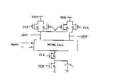
Figure 2 shows the arehiteeture of a DyCML gate according to the present
invention. The DyCML gate comprises three parts: an MCML block for logic
function evaluation, precharge transistors (Q3,Q4, Q2), an evaluation transistor (Ql)
5 with dynamic current source (C,) and an accelerating latch (Q5, Q6).
The operation is as follows: during the low phase of the clock (CLK), the
precharge transistors Q3, Q4 turn ON to charge the output nodes to VDD while
transistor Q2 turns ON to discharge capacitor Cl to GND. At the same time, transistor
Ql is OFF, elimin~ting the DC path from VDD to GND.
During the high clock phase, the precharge transistors Q2,Q3,Q4, turn off
while transistor Q, switches ON creating a current path from the two precharged
output nodes (OUT, OUT) to the capacitor Cl which acts as a virtual ground. These
two paths have different impedances depending on the logic function within the
MCML logie bloek. Therefore, one of the output nodes drops faster than the other5 node. The eross eormected transistors Q5,Q6, help to speed up the evaluation and
elimin~te the charge sharing problem whieh is charaeteristie of prior art dynamic
circuits. During the evaluation phase of operation, when one of the output node
voltages drops to less than VDD-IVTpl, the transistor whose gate is connected to this
node switches ON thereby charging the other output node to VDD again. The
20 capacitor C, is used as a virtual ground to limit the swing of the outputs and also to
cancel the DC path from VDD to GND due to the cross coupled transistors. The
value of the capacitor Cl is determined based on the value of the load capacitance (fan
out) and the required voltage swing, as discussed in greater detail below.
Transistor Q" and capacitor C" comprise a dynamic current source which
25 dramatically affects the circuit performance. At the start of the evaluation phase,
transistor Q, acts as a current source with its gate biased by VDD, driving a large
current from the MCML block. As the current charges the capacitor C" the capacitor
voltage starts to rise thereby reducing the amount of current passing through transistor
Q, until transistor Q, shuts OFF when VDS becomes zero, as shown in Figure 3. This
30 large current speeds up evaluation leading to a smaller delay and more stable
CA 0223~047 1998-04-14
operation than prior art MCML logic circuits.
Unlike most of the dynamic logic families, DyCML can function properly
over a large range of frequencies with only a small power dissipation. This is a result
of the reduced swing and the latch Q5, Q6 which elimin~tes the charge sharing
problem.
The DyCML gate of Figure 2 does not have any static power dissipation. The
power dissipation is only dynamic and is data independent because one of the output
nodes (OUT, OUT) must be low and the other node must be high whatever the logic
function is. Since the gate operation depends on a two phase clock, large clock skew
0 and slow clock transients increase the short circuit current. Increasing the width of Q2
may help avoid the effect of this short circuit current on the operation of the gate. On
the other hand, the amount of short circuit current can be decreased by reducing the
width of transistor Q, . More general solutions to this short circuit current can be
achieved using a special clock generation circuitry as described in greater detail
15 below.
The DyCML gate according to the present invention is capable of working at
low supply voltages. The lowest supply voltage is VTN +IVTPI~ This value guarantees
that during the evaluation process, the latch (Q5, Q6) will switch ON to avoid the
problems of charge sharing and hysterises.
As discussed above, the value of C, is a function of the required output swing
and the load capacitance. Since the transistor Ql passes current from the MCML
block to the capacitor until the voltage across Q" approaches zero, an approximate
value for the charge absorbed by the capacitor is
Qc =Vswillg *C, (1 )
where VSWjDg is the output voltage swing.
To obtain output swing vswillg~ an amount of charge has to pass from one of the
output nodes (OUT, OUT) to C, through the MCML block. This charge is calculated
as follows
30Q0 vswil~g C L (2)
CA 0223~047 1998-04-14
where C L iS the load capacitance per output node (including the parasitic capacitance
of the MCML block, the gate capacitance of transistors Qs~ Q6 and the parasitic
capacitances of the precharge transistors Q3, Q4).
It will be understood to a person skilled in the art that another amount of
charge flows from the second output node to Cl . This amount is much smaller than
Q0 and can be estimated to be 20% of Q0. So, the total charge passed to C, is
Q0 Vswi.. g CL 1-2 (3)
Equating (1) and (3)
Cl= CL* 1.2 (4)
& CL=FanOut (Cg+Cgd +C gs)Load +(Cg)precharge +(Cparasitic)MCML/2+(C parasitic)precharge (5)
The value of C L has to be calculated only once, then equation (5) can be used
later to calculate CL for different fan-out values. Hence, C, can be calculated using
equation (4).
The DyCML family of circuits according to the present invention can be
cascaded in many different ways. Figure 4 shows a self-timed configuration for
cascading DyCML gates. During the precharge period, the voltage at node EOE (Endof Evaluation) is zero. When the evaluation starts, current flows from the previously
charged output nodes to charge the capacitor C,. A special buffering circuit then
25 generates an SE (Start Evaluation) signal for the adjacent DyCML gate. Figure 5 is a
schematic diagram for the buffering circuit of Figure 4. For gates with many inputs,
the SE signal is obtained form the slowest input gate in order to avoid racing.
According to an alternative cascaded configuration, a clock delay architecture
can be utilized to add delay to the evaluation signals at each gate before feeding the
30 signal to the adjacent gate. Such a delay circuit would be required to be implemented
CA 0223~047 1998-04-14
for each logic level but not for each gate. One disadvantage of the proposed
alternative embodiment is that the delayed signal must be adjusted to the slowest logic
gate, thereby reducing the maximum speed of operation of the circuit.
The DyCML family of circuits according to the present invention can also be
used in pipelined configuration, through the use of an NMOS transistor (not shown)
connected to each of the output nodes, the NMOS transistors being activated during
the high phase of the clock (evaluation phase).
The pipelined configuration using NMOS transistors suffers from a significant
disadvantage however in that the outputs of the gates may not exceed VDD-V,N
0 because of the NMOS pass transistors which are used as switches. This limitation
slows down the operation of the gate and increases the minimum supply voltage of the
DyCML gate. To avoid this degradation, tr~n~mission gates can be used instead ofthe pass transistors to reduce the voltage drop across the NMOS transistors, as shown
in Figure 6.
The added tr~n~mis~ion gates increase the load capacitance and also reduce the
evaluation current. This increases the delay of the gate by a factor of 15-20%, but the
total throughput of the system is higher.
Table 1 shows the basic differences between DyCML family and some other
prior art dynamic differential logic families.
Table 1 Comparison between differential logic families
Logic Family DDL DNORA DDCVSL HRDL DDSL APL DyCML
# Transistors(inverter) 6 13 7 10 7 8
# Clockphases l l l 2 1 4 2
Logic swing VDD-VT VDD VDD VDD VDD Variant Variant
Technology NMOS CMOS CMOS CMOS CMOS CMOS CMOS
Power (swing) control NO NO NO NO NO Difficult YES
Minimum operating frequency YES NO NO YES YES NO NO
Logic type NCLT DCVS DCVS NCLT DCVS MCML MCML
Logic power source Clock VDD VDD VDD VDD VDD VDD
Reference voltage NO NO NO NO YES YES NO
Swing restorage circuit required YES NO NO NO NO NO NO
Charge sharingexists YES NO NO YES YES NO NO
Sensitive to clock skew NO NO NO YES NO YES NO
Integrabon YES YES YES YES YES YES YES
CA 0223~047 1998-04-14
As indicated above, clock generation has a major effect on the dynamic power
dissipation of the DyCML family of circuits according to the present invention. A
single ended clock generator can be designed to generate the clock signal, CLK, and
5 an inverter may be used to generate CLK . Unfortunately, this scheme increases the
clock skew and hence the power dissipation. Another approach is to use a differential
clock generator followed by a single ended termination to generate CLK and CLK, as
shown in Figure 7. The clock skew in this case is small and can be neglected. It is
common in this embodiment to use PLL's to synchronize the clock signal around the
I o chip.
In general, in order to reduce the short circuit current, the clock signal must be
as sharp as possible. Unfortunately, using such a clock signal increases the feed
through CU~ at the precharge (Q3, Q4 Q2) and evaluation transistors (Q,). This
kind of power dissipation is a function of the technology used, and cannot easily be
controlled by circuit techniques. Therefore, reducing the short circuit power
consumption requires higher clock power.
This can be overcome by using reduced swing clock signals instead of full
swing clock signals, particularly specially at the non critical precharge transistors (Q2,
Q3, Q4), without remarkable performance variation. For example, the clock used for
20 precharging transistors (Q3, Q4) may work properly if
VLOW--VDD IVTPI
Where o is a constant that determines the speed of precharging. Using larger
speeds up the precharging process. The load capacitance has to be considered when
calculating ~ because the load nodes must be charged to VDD independently of the
25 previous output state. This preFharging can not exceed 2 time where T is the clock
cycle period.
This reduced swing clock is not recommended for the evaluation transistor Q,
because it reduces the current driven through the MCML block. Hence, the delay
will increase, as discussed above. Finally, the clock power may also be reduced
CA 0223~047 1998-04-14
dramatically by decreasing the supply voltage.
The DyCML family of circuits according to the present invention has been
designed, simulated and fabricated in 0.6 ~lm (HP/MOSIS/CMC) CMOS technology.
This technology has effective channel width of 0.6 ,um and threshold voltages of5 about 0.7 and 0.9 volts for N and P transistors, as shown in Table 2. The designs are
optimized for power-delay product reduction.
CA 02235047 1998-04-14
- 10-
Table 2 Parameters o 0.5 ~m CMOS Technology
Feature NMOS PMOS
Minimum channel length 0.6 llm 0.6 llm
Minimum channel width 1.011m 1.0 llm
Effective channel width Wdrawn - o.4l~lm Wdrawn - 0.41 llm
VT 0.66 V 0.92 V
Oxidethickness 96A~ 130A~
llo 546 cm2V-Isec~l ]35 cm~V-Isec~
Cgso 305 p F/m 239 p F/m
Cgdo 305p F/m 239p F/m
Cj 562~ F/m 935~ F/m
Cjsw 50p F/m 289p F/m
A divide-by-two circuit has been designed using the pipelined version of
DyCML as shown in Figure 8. It consists of two cascaded inverters, one of which is
clocked by the CLK signal and the other being clocked by CLK. The output of the
second inverter is connected in a negative feedback manner to the input of the first
inverter to construct a toggle flip flop. This circuit has been simulated at different
operating conditions to study the performance of the DyCML configuration. The
0 voltages at different points in the pipelined DyCML inverter are shown in Figure 9 at
an input clock frequency of 1 GHz and a supply voltage of 3.3 volts.
Figure 10 shows the maximum operating frequency ofthe divide-by-two
circuit of Figure 8 versus the supply voltage. In this case, the maximum frequency is
estimated to be the frequency at which the output voltage swing will be 20% of the
supply voltage. Using the lower output swing may not result in noise immune
performance. The lower limit on the logic swing must take into consideration thevariation of the threshold of the NMOS transistors (VTN) during fabrication because if
the swing is lower than the variation in VTN incorrect results may be obtained from the
MCML logic block. Simulation results show that the divide-by-two circuit can
operate at 0.5 GHz frequency with 1.5V voltage supply and a voltage swing of 0.3volts. At 3 .3 volts, the divide-by-two circuit is capable of reaching operating speeds of
up to 2.5 GHz.
CA 0223~047 1998-04-14
As compared to prior art MCML circuits, the DyCML circuits of the present
invention are capable of achieving 43% higher frequency for a given supply voltage
and given power consumption. Figure 11 represents power/MHz, delay and power
delay product against supply voltage for the circuit of Figure 8 at 250 MHz operating
5 frequency, As expected, it can be seen that the power increases with the supply
voltage, whereas the delay decreases with increased supply voltage. However, thepower-delay product remains constant throughout the entire operating range.
Figure 12 displays power/MHz, delay and power delay product versus
operating frequency at 3.3V supply voltage. It is evident from Figure 12 that the
10 power/MHz ratio is almost constant. Since static power adds constant power
independent of frequency it is evident that there is no static power in the DyCML
circuitry according to the present invention.
A 4 bit Carry Look Ahead (CLA) adder is shown in Figure 13 which has been
used as one block of a 16 bit CLA of cascaded DyCML circuits in accordance with
5 the principles of the present invention. The logic function of the adder shown in
Figure 13 is
G = G3 + P3G2 + P3P2G, + P3P2P~Go
The adder is constructed using four such blocks, as shown in Figure 14. Each
block provides the necessary block generate and block propagate signals that may be
20 used for a second CLA level, rather than the single level shown in Figure 14. Test
results have indicated that, when compared to a standard CMOS implementation of
the same circuit, with ideal SCMOS circuits and synchronized inputs and stable power
supply, a 40% reduction in power dissipation and 50% reduction in delay were
obtainedwiththeDyCMLconfigurationofFigures 13 and 14(i.e. 30%ofthepower
25 delay product of the standard prior art CMOS implementation).
To summarize, a new logic family (DyCML) is provided according to the
present invention. A major advantage of the DyCML family is the provision of
controllable-output swing, and hence power consumption. Also, the use of a dynamic
current source provides shorter delays compared with prior art MCML circuits. Other
30 advantages inherited from MCML are high-performance, low supply voltage, low
CA 0223~047 1998-04-14
noise and low jitter. The DyCML family of circuits is easy to pipeline or cascade in
both synchronous and asynchronous modes. It is also suitable for portable computers
and wireless communication systems and for critical paths in complex microprocessor
systems and multimedia applications where low power is required with high
5 throughput. The DyCML circuitry according to the present invention is also suitable
for fabrication using Multiple Threshold CMOS technology (MTCMOS), wherein the
precharge transistors are implemented using high VT while the remainder of the
circuitry is implemented using low VT transistors for increased speed.
Other embodiments, modifications and applications of the invention are
0 possible. All such variations and applications are believed to be within the sphere and
scope of the invention as defined by the claims appended hereto.