Language selection

Search

Patent 2235658 Summary

Third-party information liability

Some of the information on this Web page has been provided by external sources. The Government of Canada is not responsible for the accuracy, reliability or currency of the information supplied by external sources. Users wishing to rely upon this information should consult directly with the source of the information. Content provided by external sources is not subject to official languages, privacy and accessibility requirements.

Claims and Abstract availability

Any discrepancies in the text and image of the Claims and Abstract are due to differing posting times. Text of the Claims and Abstract are posted:

  • At the time the application is open to public inspection;
  • At the time of issue of the patent (grant).
(12) Patent: (11) CA 2235658
(54) English Title: ELECTRONIC BALLAST CIRCUIT
(54) French Title: CIRCUIT DE BALLAST ELECTRONIQUE
Status: Expired and beyond the Period of Reversal
Bibliographic Data
(51) International Patent Classification (IPC):
  • H05B 41/14 (2006.01)
  • H05B 41/24 (2006.01)
  • H05B 41/26 (2006.01)
  • H05B 41/295 (2006.01)
(72) Inventors :
  • FOO, ONN FAH (China)
(73) Owners :
  • MASS TECHNOLOGY (H.K.) LTD.
(71) Applicants :
  • MASS TECHNOLOGY (H.K.) LTD. (China)
(74) Agent: RICHES, MCKENZIE & HERBERT LLP
(74) Associate agent:
(45) Issued: 2004-08-10
(22) Filed Date: 1998-04-23
(41) Open to Public Inspection: 1999-07-19
Examination requested: 2001-09-10
Availability of licence: N/A
Dedicated to the Public: N/A
(25) Language of filing: English

Patent Cooperation Treaty (PCT): No

(30) Application Priority Data:
Application No. Country/Territory Date
98104011.X (China) 1998-01-19

Abstracts

English Abstract


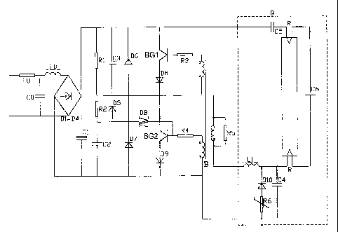
An electronic ballast circuit for fluorescent lamps, said circuit comprises an
anti-interfering circuit, a rectifying circuit, a filtering circuit, a
frequency-converting
circuit and a resonant circuit connected sequentially; a main
resonant capacitor C4 is connected between the end of the the fluorescent lamp
connected with the resonant inductor L1 in the resonant circuit and the
negative
end of the filtering circuit, so that resonant inductor L1 and main resonant
capacitor C4 constitute a main resonant circuit; the Q factor of the main
resonant circuit is not affected by the resistance of the filaments at both
ends of
the fluorescent lamp, so that the voltage applied across borh ends of the lamp
can be raised; and a preheating circuit is provided between both two ends of
the main resonant capacitor, so that the filaments of the lamp can be
preheated
before the lamp is started.
6


Claims

Note: Claims are shown in the official language in which they were submitted.


What is claimed is:
1. An electronic ballast circuit for a fluorescent lamp having filaments,
comprising:
an anti-interfering circuit, a rectifying circuit, a filtering circuit, a
frequency-converting circuit and a series resonant circuit connected
sequentially,
said series resonant circuit consisting of a first resonant capacitor, the
resistance of
the filaments of said fluorescent lamp and a resonant inductor connected in
series,
said fluorescent lamp having a first end and a second end, characterized in
that a
second resonant capacitor (C4) is directly connected between said first end of
said
fluorescent lamp which is connected with said resonant inductor (L1) in said
series
resonant circuit and a negative end of said filtering circuit, so that said
resonant
inductor (L1) and said second resonant capacitor (C4) constitute a main
resonant
circuit, and, in a high frequency AC loop, wherein voltage across both ends of
said
second resonant capacitor (C4) being the starting voltage of said lamp, and
wherein
a preheating circuit is connected in parallel between both ends of said second
resonant capacitor (C4) in said main resonant circuit, said preheating circuit
being
an integrally sealed assembly.
2. The electronic ballast circuit according to claim 1, characterized in that
said
preheating circuit consists of a diode (D10) and a PTC thermistor (R6)
connected in
series.
3. The electronic ballast circuit according to claim 1, characterized in that
said
preheating circuit consists of two diodes (D11)-(D12) and a PTC thermistor
(R6)
connected in series.
4. The electronic ballast circuit as described in Claim 2 or 3, characterized
in that a
common electric resistance is used instead of said PTC thermistor R6.
5. The electronic ballast circuit as described in Claim 2, characterized in
that said
diodes D10 and PTC thermistor R6 are fabricated as an integrally sealed
assembly.
6. The electronic ballast circuit as described in Claim 3, characterized in
that said
diodes D10, D12 and PTC thermistor R6 are fabricated as an integrally sealed
assembly.
5

Description

Note: Descriptions are shown in the official language in which they were submitted.


CA 02235658 1998-04-23
ELECTRONIC BALLAST CIRCUIT FOR FLUORESCENT LAMPS
The present invention relates to an ignite or control circuit device for
discharge lamps, more particularly, the present invention relates to an
electronic ballast circuit for fluorescent lamps.
Electronic ballast circuits for fluorescent lamps usually adopt a series
resonant circuit, that is to say, a resonant circuit consisting of a
capacitor, the
resistances of the filaments and an inductor connected in series is used to
produce a high voltage across the ends of the fluorescent lamp to ignite it,
and a
rectifying circuit, a filtering circuit and a frequency-converting circuit are
sequentially connected between the power supply and the series resonant
circuit, with an optional anti-interfering circuit provided before the
rectifying
circuit in some of the electronic ballast circuits. In this kind of electronic
ballast
circuit, the resistance of the filaments of the fluorescent lamp might reduce
the
Q factor of the series resonant circuit, which causes the resonance voltage to
be
insufficient to ignite the fluorescent lamp, and the lamp will be difficult to
start;
if the lamp is directly ignited with the filamznts resistance shorted, the
lamp is
started without preheating the filaments, and the life of the filaments of the
fluorescent lamp will be significantly reduced by this kind of cold cathode
starting; moreover, this kind of existing electronic ballast circuit is
suitable to a
power supply of 200-240 volts, when the voltage of the power supply is 100-
120 volts, the resonant voltage thereof cannot meet the requirement for the
normal igniting of the fluorescent lamp.
The object of the present invention is to overcome the disadvantages of
the above conventional electronic ballast circuits, and to provide an
electronic
ballast circuit for fluorescent lamps which has high Q factor and high
resonance
voltage .
To realize this object, the following technical scheme is adopted: the
ballast circuit includes, an anti-interfering circuit, a rectifying circuit, a
filtering circuit, a frequency-converting circuit and a resonance circuit
connected sequentially, the resonance circuit comprises a resonant capacitor,
the resistance of the filaments of the fluorescent lamp, and a resonant
inductor
connected in series, characterised in that, in the resonant circuit,a main

CA 02235658 2003-06-11
resonant capacitor is provided between the end of the fluorescent lamp
connected
with the resonant inductor and the negative end of the filtering circuit. so
that the
resonant induc;tor and the main resonant capacitor form a main resonant
circuit, and
in the high frequency AC loop, the voltage across the ends of the main
capacitor is
just the starting voltage between the ends of the fluorescent tube.
Since the present invention utilizes the resonant inductor of the resonance
circuit, and a main capacitor is provided between the end of the fluorescent
lamp
connected with the resonant inductor and the negative end of the filtering
circuit,
the Q factor of the main resonant circuit will not be affected by the
resistance of the
filaments at both ends of the fluorescent lamp, so the voltage applied to the
ends of
the lamp can be raised.
Accordingly, in one aspect, the present invention provides an electronic
ballast circuit for a fluorescent lamp having filaments, comprising: an
anti-interfering circuit, a rectifying circuit, a filtering circuit, a
frequency-converting circuit and a series resonant circuit connected
sequentially,
said series resonant circuit consisting of a first resonant capacitor, the
resistance of
the filaments of said fluorescent lamp and a resonant inductor connected in
series,
said fluorescent lamp having a first end and a second end. characterized in
that a
second resonant capacitor (C4) is directly connected between said first end of
said
fluorescent lamp which is connected with said resonant inductor (L1) in said
series
resonant circuit and a negative end of said altering circuit, so that said
resonant
inductor (L 1 ) and said second resonant capacitor (C4) constitute a main
resonant
circuit, and, in a high frequency AC loop, wherein voltage across both ends of
said
second resonant capacitor (C4) being the starting voltage of said lamp, and
wherein
a preheating .circuit is connected in parallel between both ends of said
second
resonant capacitor (C4) in said main resonant circuit, said preheating circuit
being
an integrally sealed assembly.
2

CA 02235658 2003-06-11
The invention is further described i.n detail with reference to the
appended figures and embodiments, in which:
Fig. 1 is a biiock diagram illustrating an electronic ballast circuit of the
prior
art.
Fig. ? is a block diagram illustrating another electronic ballast circuit of
the
prior art.
Fig. is a schematic diagram illustrating the principle of the present
invention.
Fig. 4 shows the waveform of the electric current passing through the
fluorescent lamp during the starting process.
Fig. ~ shows the wavefornn of the voltage across the tZuorescent tube
during the starting process.
F ig. b shows the waveform of the voltage across the ends cf PTC
thermistor R6 during the starting process.
Fi~.~. ~' shows the waveform of the electric current passing throuffll FTC
then-rlistor Rb C~'.lrlll~ the starting process.
Fib,. 3 is another schematic diagram of the preheating circuit cf the present
invention.
<~s shown in Fig.l, tile conventional elec~:ronic ballast circuit <Tenerallv
has
the tollewin~> >tr~:cture: an anti-interferin~~ circuit, a rectifvin~~
~;.;rcuit, a tiitenng
circuit and a ~ equencv-converting circuit are sequentially connected to the
?a

CA 02235658 1998-04-23
input of the 220 V power supply, and a series resonant circuit is provided
after
the frequency converting circuit, said resonant circuit includes resonant
capacitors C5, C6 and resonant inductor L1, with the resistance of the
filaments at both ends of the lamp also connected in series in the resonant
circuit. This kind of resonant circuit is well known to those skilled in the
art,
the Q factor of the series resonant circuit would be decreased by the effect
of
the resistance of the filaments at the ends of the fluorescent lamp, which
causes
the resonance voltage to be insufficient to start the lamp. Moreover, most of
these circuits are designed for using with a 220 ~ 20 V power supply, if the
voltage of the power supply is 110 ~ 10 V, the lamp will be even more
difficult
to start. To solve the problem in starting the lamp, one method is to have the
resistances of the filaments at both ends of the lamp short-circuited as shown
in
Fig.2, this will raise the Q factor of the series resonant circuit and, with
it, the
voltage between the ends of the lamp, thus starting the lamp. However, the
disadvantage of thus doing is that the filaments have not been preheated, the
lamp is directly started with cold cathode, and the life of the lamp will be
significantly reduced, so it is not a preferable method to solve the problem.
With reference to Fig.3 and comparing with Fig.l, the anti-interfering
circuit consists of CO and L0; the rectifying circuit consists of diodes D 1-
D4;
the filtering circuit consists of filtering capacitor C 1; the frequency-
converting
circuit consists of resistances Rl-R4, capacitors C2-C3, diodes DS-D9,
transistors BG1-BG2, bidirectional silicon-controlled rectifier DB, and
transformer B; the series resonant circuit consists of capacitors CS-C6, the
resistances of the two filaments 2R, and resonant inductor L 1, while the main
resonant circuit consists of resonant inductor L 1 and main resonant capacitor
C4, as shown in the region surrounded by dash lines in Fig. 3, one end of
capacitor C4 is connected to the node of the inductor L 1 and the fluorescent
lamp, the other end of capacitor C4 is connected to the negative end of
filtering
capacitor C1 (the end 5 of the primary winding of transformer B). As can be
seen from Fig. 3, for the high frequency AC loop, the voltage across both ends
of the main capacitor C4 equals to the voltage across the ends of the
fluorescent lamp, thus preventing the Q factor of the main resonant circuit
from
being effected by the resistance of the filaments, so that the lamp can be
normally started. To preheat the filaments at both ends of the fluorescent
lamp,
a preheating circuit is provided between both ends of the main resonant
3

CA 02235658 1998-04-23
capacitor C4, the preheating circuit consists of diode D 10 and PTC thermistor
R6 connected in series, when starting the lamp, the high voltage between both
ends of C4 is subject to the unidirectional clamping of the diode D10 and PTC
thermistor R6 in the preheating circuit, thus the voltage across C4 is made
comparatively low, the lamp cannot be started owing to the voltage across the
fluorescent lamp being lower than the ignite voltage and, at this time, the
current preheats the filaments . When the temperature of PTC thertnistor R6 is
raised above a lower limit , the voltage across the lamp is raised
correspondingly, and the lamp is started. The waveform of the current passing
through the fluorescent lamp and the waveform of the voltage across the lamp
during the starting process are shown in Fig.4 and Fig. 5, respectively. Once
the lamp operates normally, as can be seen from Fig.7, the current passing
through PTC thermistor R6 is very small, thus the power consumption in the
PTC thermistor R6 itself is very low, because diode D 10 is at a state of high
electric level, its conducting angle is very small (the voltage across PTC
thermistor R6 is shown in Fig.6).
With reference to Fig.B, the preheating circuit may also consist of two
diodes ~ D 11-D 12 and PTC thermistor R6 connected in series, the two diodes
are placed in the circuit in the same polarity, and the PTC thermistor R6 is
located between diodes D 11 and D 12. Of course, the manner of connecting the
PTC thermistor R6 is not limited to this, PTC thermistor R6 may be connected
to the anode of diode Dl 1 or to the cathode of diode D12. And PTC thermistor
R6 may be replaced by a common resistor.
In fabricating, the preheating circuit may be designed as an integrally
sealed assembly, that is to say, the serially connected diode and thermistor
are
integrally sealed in a package , so that it will be easier to install , to
connect,
and to form the final product.
4

Representative Drawing
A single figure which represents the drawing illustrating the invention.
Administrative Status

2024-08-01:As part of the Next Generation Patents (NGP) transition, the Canadian Patents Database (CPD) now contains a more detailed Event History, which replicates the Event Log of our new back-office solution.

Please note that "Inactive:" events refers to events no longer in use in our new back-office solution.

For a clearer understanding of the status of the application/patent presented on this page, the site Disclaimer , as well as the definitions for Patent , Event History , Maintenance Fee  and Payment History  should be consulted.

Event History

Description Date
Time Limit for Reversal Expired 2012-04-23
Letter Sent 2011-04-26
Inactive: IPC from MCD 2006-03-12
Grant by Issuance 2004-08-10
Inactive: Cover page published 2004-08-09
Pre-grant 2004-05-17
Inactive: Final fee received 2004-05-17
Notice of Allowance is Issued 2003-12-22
Letter Sent 2003-12-22
Notice of Allowance is Issued 2003-12-22
Inactive: Approved for allowance (AFA) 2003-12-05
Amendment Received - Voluntary Amendment 2003-06-11
Inactive: S.30(2) Rules - Examiner requisition 2002-12-20
Letter Sent 2001-10-11
Request for Examination Requirements Determined Compliant 2001-09-10
All Requirements for Examination Determined Compliant 2001-09-10
Request for Examination Received 2001-09-10
Inactive: Cover page published 1999-11-22
Application Published (Open to Public Inspection) 1999-07-19
Inactive: Single transfer 1998-08-31
Inactive: IPC assigned 1998-07-21
Classification Modified 1998-07-21
Inactive: IPC assigned 1998-07-21
Inactive: First IPC assigned 1998-07-21
Inactive: Courtesy letter - Evidence 1998-07-14
Inactive: Filing certificate - No RFE (English) 1998-07-07
Application Received - Regular National 1998-07-03

Abandonment History

There is no abandonment history.

Maintenance Fee

The last payment was received on 2003-12-11

Note : If the full payment has not been received on or before the date indicated, a further fee may be required which may be one of the following

  • the reinstatement fee;
  • the late payment fee; or
  • additional fee to reverse deemed expiry.

Patent fees are adjusted on the 1st of January every year. The amounts above are the current amounts if received by December 31 of the current year.
Please refer to the CIPO Patent Fees web page to see all current fee amounts.

Owners on Record

Note: Records showing the ownership history in alphabetical order.

Current Owners on Record
MASS TECHNOLOGY (H.K.) LTD.
Past Owners on Record
ONN FAH FOO
Past Owners that do not appear in the "Owners on Record" listing will appear in other documentation within the application.
Documents

To view selected files, please enter reCAPTCHA code :


To view images, click a link in the Document Description column (Temporarily unavailable). To download the documents, select one or more checkboxes in the first column and then click the "Download Selected in PDF format (Zip Archive)" or the "Download Selected as Single PDF" button.

List of published and non-published patent-specific documents on the CPD .

If you have any difficulty accessing content, you can call the Client Service Centre at 1-866-997-1936 or send them an e-mail at CIPO Client Service Centre.

({010=All Documents, 020=As Filed, 030=As Open to Public Inspection, 040=At Issuance, 050=Examination, 060=Incoming Correspondence, 070=Miscellaneous, 080=Outgoing Correspondence, 090=Payment})


Document
Description 
Date
(yyyy-mm-dd) 
Number of pages   Size of Image (KB) 
Representative drawing 1999-10-17 1 7
Description 2003-06-10 5 266
Claims 2003-06-10 1 52
Drawings 2003-06-10 3 39
Abstract 1998-04-22 1 25
Claims 1998-04-22 1 51
Description 1998-04-22 4 237
Drawings 1998-04-22 3 38
Representative drawing 2004-07-06 1 9
Filing Certificate (English) 1998-07-06 1 174
Courtesy - Certificate of registration (related document(s)) 1998-10-26 1 114
Reminder of maintenance fee due 1999-12-28 1 113
Acknowledgement of Request for Examination 2001-10-10 1 194
Commissioner's Notice - Application Found Allowable 2003-12-21 1 160
Maintenance Fee Notice 2011-06-06 1 171
Correspondence 1998-07-13 1 29
Fees 2003-04-09 1 38
Fees 2003-12-10 1 37
Fees 2000-04-10 1 40
Fees 2002-04-15 1 37
Fees 2001-04-11 1 40
Correspondence 2004-05-16 1 35
Fees 2005-04-12 1 33
Fees 2006-04-09 1 35
Fees 2007-04-10 1 44
Fees 2008-03-19 1 48
Fees 2009-03-31 1 62
Fees 2010-03-29 1 51