Note: Descriptions are shown in the official language in which they were submitted.
CA 02236260 1998-04-29
A light conducting plate, method for
m~kin~ the same and using thereof
Field nf the invention
The present invention relates to a light conducting plate and the use
thereof and more particular to a light conducting product and a method
for making the same.
Back~round of the invention
o Light conducting fiber was reported in 1950's and got on with practical
application in 1960's. Light conducting fiber is comprised of a light
conducting layer of high refrangibility and a light reflecting layer of low
refrangibiligy coated thereon. When light enters into the f1ber from one
side, total reflection takes place in the interface between the light
conducting layer and the light reflecting layer many times and light exits
from the other side of the fiber. Because light conducting fiber has
excellent light transmission performance and is able to conduct light in
flexible state, it has been widely used for information transmission field.
For many years, research efforts have been devoted to opening up new
fields of the application of light conducting fiber. Up to now, for the
sake of limitations of its construction, no achievement has been made.
It is an object of the present invention to provide a light conducting plate
which has a good light transmission performance and an ability of
transmitting light multidirectionally.
CA 02236260 1998-04-29
It is another object of the present invention to provide a novel light
conducting product which transmits light from a light source
multidirectionally and release it at predetermined places to obtain
expected display.
The other aspects of the present invention will be illustrated in the
following description.
o Sllmm~ry ofthe invention
A light conducting plate consists of a light conducting layer and light
reflecting layers. The upper and lower surfaces of the light conducting
layer are coated with the light reflecting layers.
According to the present invention, a light conducting product includes
a light conducting layer and light reflecting layers coated on the upper
and lower surfaces of said light conducting layer, wherein at least one of
the two light reflecting layers is provided with a certain pattern so that a
part of the light conducting layer is covered with the light reflecting
layer.
Brief description of the drawin~
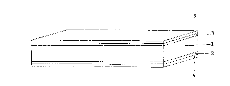
Fig. 1 is a structural schematic diagram of a five-layer light conducting
plate of the present invention.
Detailed desçription of the invention
CA 02236260 1998-04-29
In order to make use of light transmission characteristic of light
conducting material and extend the application of the same, the inventor
has developed a light conducting plate having a characteristic of
transmitting light multidirectionally. The light conducting plate
comprised of a light conducting layer and light reflecting layers, wherein
the light reflecting layers are coated on two opposite surfaces of the light
conducting layer to form a three-layer plate.
Among light conducting materials for light conducting layer are
o transparent materials of high refrangibility. Commonly used materials
are transparent polystyrene and organic glass with polystyrene being
preferred. Among light reflecting materials for light reflecting layers are
transparent polymers of low refrangibility which are compatible with
light conducting materials for light conducting layer, such as polymethyl
methacrylale ( organic glass) or metallic films which can produce total
reflection, e.g. metallic Al, Ti-Au or Cr and the like. Thus, total
reflection takes place in the interfaces between the light conducting layer
and light reflecting layers to minimi7e light transmission loss.
The light conducting plate of the present invention may comprise an
opaque layer (shielding layer) coated on the light reflecting layers. It can
be coated either on one or both of the light reflecting layers which are
coated on both surfaces of the light conducting layer. Preferably, an
opaque layer is coated on two light reflecting layers to form a five-layer
light conducting plate. The materials for opaque layer may be various
resin paints, which can be used individually or as a mixture thereof.
CA 02236260 1998-04-29
Light-tight resin film(s) also can be used for opaque layer. For example,
commonly used materials are light-tight ABS resin film, ABS resin/PC
resin ( polycarbonate resin ) alloy film or PVC(polyvinylchloride) resin
film. The materials used for opaque layers coated on both surfaces of the
s light conducting plate may be the same or different. The opaque layer
may be used not only to shield the plate from light but also to protect the
light reflecting layer. If desired, the opaque layer coated on one surface
of light reflecting layers may comprise of two or more layers.
o According to the present invention, the size and shape of said light
conducting plate may be selected optionally as re~uired. Generally, the
thickness of said light conducting layer (central layer)and that of the
light reflecting layers are about 3-15 mm and about 0.03-0.25 mm
respectively. The thickness of two light reflecting layers may be the
same or different. The thickness of opaque layers coated on two surfaces
of light conducting layer ranges from 0.1 to 0.25 mm and may be the
same or different.
In the light conducting plate of the invention, there is no light reflecting
materials coated on both side ends or at least one of the side ends or a
part of one side end. When a light source is provided at one side end of
the light conducting plate, light will be transmitted into and through the
light conducting layer multidirectionally. Because total reflection takes
place in the interfaces between the light conducting layer and light
reflecting layers, light is transmitted therein with a low loss.
CA 02236260 1998-04-29
According to the present invention, a composite light conducting plate
can be prepared by 1~1nin~ting, for example, two or more three-layer
light conducting plates or interposeing one or more opaque layers
between two light reflecting layers l~min~ted together so as to meet
various needs. Similarly, opaque layer may be also coated on the outest
surfaces of the composite light conducting plate for different uses.
The following methods may be used to prepare the light conducting
plate of the present invention:
1. Coating:
Light reflecting materials which are compatible with the light
conducting materials are coated on a plate used for light conducting
layer to obtain the light conducting plate of the present invention. For
example, a polystyrene plate is placed horizontally and one of the
surfaces of the plate is sprayed ( or brushed) with ethanol-acetlc acid
solution of polymethyl methacrylate, and then the plate is dried at 55~C-
65~C. In the same manner, the other surface of the plate is then coated
with polymethyl methacrylate. The polystyene plate coated with
polymethyl methacrylate on both surfaces is the three-layer light
conducting plate of the invention. If required, light-tight resin paints can
be sprayed ( or brushed) on the outer surfaces of polymethyl
methacrypate layers to obtain a four or five-layer light conducting plate.
Preparation of ethanol-acetic acid solvent: 2-4 parts of acetic acid is
added to 1 part of ethanol (V/V), then shake the mixture to
CA 02236260 1998-04-29
homogeneous state to obtain the solvent.
Preparation of ethanol- acetic acid solution of polymethyl methacrylate:
6-15 L ethanol-acetic acid solvent above is added to lKg polymethyl
methacrylate molding powder to form a mixture. The mixture is stirred
up until the resin is completely dissolved to obtain ,the title solution.
2. Deposition:
Light reflecting materials such as metallic film are deposited on a plate
o for light conducting layer to obtain a light conducting plate of present
invention. For example, after a polystyrene plate is placed in a vacuum
deposition device, the two surfaces of the polystyrene plate are deposited
with Al film, thereby a three-layer light conducting plate having is
provided. If needed, light-tight resin paints can be sprayed( or brushed )
on the outer surface(s) of Al film to obtain a light conducting plate
having four or five layers of the present invention.
3. Coextrusion:
Coextrusion is a process capable of laminating three or more layers, e.g.
five layers by using a composite plate coextrusion machine to produce a
composite plate having three or more layers of the present invention in a
single operation. In illustration of a five-layer light conducting plate, the
light conducting layer is of polystyrene while two light reflecting layers
are of polymethyl methacrylate and two opaque layers are of ABS resin
or ABS/PC resin alloy or PVC resin. A five-layer light conducting plate
of the present invention can be produced by introducing the
CA 02236260 1998-04-29
aforementioned materials into the composite plate coextrusion rnachine
and being coextruded in a single operation.
The light conducting plate of the present invention finds wide utilities,
s especially for manufacturing signboards, billboards and instrument
panels. The method comprises engraving characters (letters) or patterns
on the light conducting plates manually or by a carving machine. During
the process of engraving, a part of light reflecting layer and/or opaque
layer on the light conducting plate is cut out according to the shape and
o size of characters or patterns, which, if needed, can be carried out on one
or two surfaces of the light conducting plate. If a pattern is of a special
shape, the preparation of signboards, billboards and instrument panels
may be performed by hot-pressing in dies. In engraving operation, parts
of the light conducting layer may be cut off, but the depth to be cut
should be no more than 2/5, preferably no more than 1/5 of the total
thickness of the same. When a light source is provided at the side of the
light conducting plate, the characters and patterns will emit eye-catching
light. If fluorescent paints are coated on the parts cut off, colorful
signboards, billboards and instrument panels may be prepared.
The light conducting plate of the present invention has superior light
transmission characteristics and lower attenuation during light
transmission, is capable to transmit light in flexible plate and can be
easily prepared with a light weight and a low cost.
The light conducting plate of the present invention may be prepared
CA 02236260 1998-04-29
manually or on a large scale simply with a low cost.
Signboards, billboards and instrument panels made from the light
conducting plate of the present invention have many advantages: a high
s light signal, prominent headlines, high efficiency, economic power, good
decoration, long duration, simplified construction, a light weight, small
volume and the like. The total thickness of a double-faced billboard can
be controlled ranging from 3-5 mm only.
o A light conducting product comprises of a light conducting layer and
light reflecting layers which are coated on both surfaces of said light
conducting layer, wherein at least one light reflecting layer is coated on
said light conducting layer as a specific pattern so that a part of said
surface of said light conducting layer is covered. When a light source is
provided at the side end of the light conducting layer, light will be
transmitted multidirectionally therethrough and exit from the light
conducting layer at a position where the light conducting layer is not
coated by the light reflecting layer. Because the uncoated part has a
special pattern, light will emit and show the same.
An opaque layer can be coated on the light reflecting layer of said light
conducting product. As the light reflecting layer has a special pattern,
the opaque layer coated thereon also has a corresponding pattern.
A light conducting product includes the light conducting plate of the
present invention, wherein on at least one surface of said light
CA 02236260 1998-04-29
conducting plate, a part of light reflecting layer or a part of opaque layer
and light reflecting layer are carved and cut off according to a pattern so
that said pattern of light conducting layer reveals itself. If required, a
pattern can be penetrated into the light conducting layer or a part of light
s conducting layer can be cut off according the pattern, but the depth to be
cut should be no more than 2/5, preferably no more than 1/5 of the
thickness of light conducting layer.
A display device including light source and the light conducting plate of
o the present invention, wherein light is provided from at least one side
end of said light conducting plate to the light conducting plate, said light
conducting plate comprises light conducting layer and light reflecting
layers coated on two opposite surfaces of said light conducting layer,
wherein the light conducting layer is covered partially by at least one of
s the light reflecting layers so that a special pattern may manifest itself on
said surface of said light conducting layer.
Similarly, an opaque layercan be coated on the light reflecting layer.
When the light reflecting layer has a special pattern, the opaque layer
will show the same. Light from the light conducting layer will exit to
show the pattern.
A display device including a light source and light conducting plate of
the present invention, wherein light is provided from at least one side
end of said light conducting plate to the light conducting layer and a part
of light reflecting layer or a part of opaque layer and light reflecting layer
CA 02236260 1998-04-29
on at least one surface of said light conducting layer are carved and cut
off according to the shape or size of a pattern, thereby said pattern
reveals itself on the light conducting layer. If it is required, a pattern can
penetrated into the light conducting layer or a part of the light
conducting layer is cut off according to the pattern, but the depth to be
cut off is no more than 2/S, preferably no more than 1/S of the thickness
of the light conducting layer. When light from a light source is provided
to the light conducting layer, it is released through said pattern so that
the said pattern is clearly discernible at night or in the dark.
Example 1. Preparation of the light conducting plate of the present
invention by coating.
A polystyrene plate (Smm thick) was cut to a rectanglar shape of 600
mm x400 mm. Then the plate was placed horizontally on a shelf,
sprayed with ethyl alcohol-acetic acid solution of polymethyl
methacrylate and dried at 55~C - 65~C. Next it was turned over and
sprayed with ethyl alcohol-acetic acid solution of polymethyl
methacrylate in the aforementioned manner and dried to obtain a three-
layer light conducting plate of the present invention. Ethyl alcohol-acetic
acid solution of polymethyl methacrylate was prepared by adding 9L of
ethyl alcohol-acetic acid solution into 1 Kg molding powder of
polymethyl methacrylate. The ethnol-acetic acid solution was formulated
by adding three parts of ethyl alcohol to seven parts of acetic acid (v/v)
and mixing resulting solution.
Example 2. Preparation of the light conducting plate of present invention
CA 02236260 1998-04-29
by deposition method
Polystyrene plate (lOmm thick) was cut to a rectanglar shape of
600x400mm and placed in a vacuum aluminum deposition apparatus.
Then, a 0.03 mm Al film is deposited on both surfaces of the polystyrene
plate to obtain a three-layer light conducting plate. In order to protect
Al-film from abrasion and scratch, a resin paint was coated on the two
outer surfaces of the Al-film as a shielding and protecting layer, thereby
a light conducting plate having five layers of the present invention was
obtained.
Example 3. Preparation of the light conducting plate of the present
invention by coextrusion moulding
A five-layer light conducting plate of the present invention was prepared
by coextrusion in a single operation through a composite plate
coextrusion machine capable of l~lnin~ting five layers. See Fig. 1.
The process comprises the following steps:
Granular material of polystyrene was added into No. 1 feed hopper of the
composite plate coextrusion machine. The molten (softening)
polystyrene was extruded from extruder No.1 into coextrusion die and
passed through a gap for light conducting layer of the coextrusion die to
form a light conducting layer (1).
Granular material of polymethyl methacrylate was added into No.2 and
No.3 feed hoppers. The resulting molten (softening) polymethyl
c~ _~
! CA 02236260 1998-04-29
methacrylate was extruded from extruders No.2 and No.3 into
coextrusion die and passed through two gaps for light reflecting layers
so as to be formed on two surfaces of the light conducting layer (1) to
obtain two light reflecting layers (2,3).
Granular material of light-tight ABS resin (or ABS/PC resin, PVC resin)
was placed into No.4 and No.5 feed hoppers. The molten (softening)
ABS resin was extruded from extruders No.4 and No.S into coextrusion
die and passed through two gaps for light protecting material so as to be
o formed on two outer surfaces of light reflecting layers (2,3) to obtain
opaque layers (4,5).
Extruders No. 1, 2, 3, 4, 5 were operated simultaneously. Three
different starting materials were extruded into coextrusion die and then
passed through different passages respectively to form a composite sheet.
Then it is pressed by a three-roll calender roller, cooled, drawn, trimmed
and cut to obtain a five-layer light conducting plate of the present
invention.
If No.4, 4 feed hoppers and No.4, 5 extruders are not used, a three-layer
light conducting plate of the present invention can be obtained.
Example 4. Preparation of light conducting signboards or billboards with
the light conducting plate of the present invention.
1. A three-layer light conducting plate with a 5 mm light conducting
CA 02236260 1998-04-29
layer prepared by coating was cut into a rectanglar shape of
600mmx400mm. "Instant sticking" used as opaque layers was sticked
on both surfaces of the light conducting plate. The "instant sticking" and
reflecting layer were cut off by a carving machine to form an expected
pattern. The cutting depth penetrated into light conducting layer was no
more than 0.5mm. Light sources with lambshades ~,vere installed on two
side ends of the light conducting plate to obtain a light conducting
signboard or billboard. Only two 15w fluorescent lamps were needed to
be installed on two sides of the board. Characters and patterns made by
10 this way were very bright and eye-catching. Said signboard made by the
present invention has a simple construction, a light weight and lower
costs.
2. A five-layer light conducting plate prepared by coating was cut to
600mmx400mm. According to the shape or size of a pattern, the resin
paint of the protective opaque layer and polymeth~Tl methacrylate of the
reflecting layer were cut out, but the depth penetrated into the layers was
no more than 0.5mm. Two 1 Sw fluorescent lamps were installed one two
side ends of the light conducting plate. Characters and patterns engraved
by this method were very bright and eye-catching. If fluorescent paints
of different colors are coated on the parts carved, the signbilld of light
conducting late would be colorful and very beautiful. Said light
conducting signboard is convenient to produce and simple in
construction with a light weight, a low cost and reduced power. It is
superior to a lamp box.
CA 02236260 1998-04-29
3. The light conducting plate having five layers prepared by deposition
method was used in the preparation of light conducting billboards in the
same manner as the examples above. The similar result was obtained.
Example 5. Preparation of instrument panel for cab of motorvehicle with
the light conducting plate made by a coextrusion moulding method of
the present invention.
A light conducting plate having a 3mm thick light conducting layer and
o a opaque layer of ABS resin was cut to a required shape. The required
characters and patterns were cut out by a computer-based carving
machine. The cutting reached light conducting layer. Then the plate was
placed in a mold and formed into an instrument panel with a required
shape by hot pressing. Fluorescent paint of different colors was coated
on carved parts to obtain a light conducting instrument panel. Small
min~nt were mounted on the sides of the panel to enable the panel to
display clearly. Said motor-vehicle instrument panel is compact, simple,
less power consuming, easy to produce with a low cost, a beautiful
appearance and a long duration.