Note: Descriptions are shown in the official language in which they were submitted.
CA 02236688 l998-0~-04
W O 97~6884 PCT/SE96J01407
DEVICE AND M~THOD OF SUPPLYING FROM AN AC SOURC~
FIELD OF INrVENrrION
The present invention relates to the field of voltage
converters and more particularly to the field of converting
alternating voltage to a continuous voltage or direc~ current
voltage. More specifically, the invention relates to an
arrangement and ~o a method for measuring minimum input
voltage, the transformer TR1 is supplied with current mainly
by the capacitors in the two valley-fill circuits 12, 14.
DESCRIPTION OF TXE PRIOR ART
IEC 1000-3-2 is a standard which discloses what appearance?
the voltage input and current input to an arrangement from an
alternating voltage source shall have in order to be classed
as a class A-type apparatus. One such arrangement is
described in DE-A-4 243 943, among other things. The
arrangement described in this publication includes a
capacitor which is charged during that time period in which
the absolute value of the source voltage exceeds the voltage
across the capacitor, and is discharged when the absolute
value of the source voltage is below this voltage.
Another arrangement which fulfils the requirement of the
aforesaid standard is described in the article "A New Family
of Single-Stage Isolated Power-Factor Correctors with Fast
3Q Regulation of the Output Voltage", by R. Redl, L. Balogh and
N.O. Sokal in PESC 94, Record, pages 1137-1144. This document
is concerned mainly with how two switches can be combined to
CA 02236688 1998-0~-04
W O 97/16884 PCT/SE96/01407
form one ewitch. The document discloses a plurality of
different converter circuits. One of these circuits is a
voltage converter that includes a rectifier bridge whose one
output terminal is connected to a coil which, in turn, is
connected to a valley-fill circuit. The valley-fill circuit
is connected to a fly-back converter which includes three
windings. A controllable switch is connected between the
other output terminal of the rectifier bridge and the
interconnection junction between the coil and the valley-fill
circuit. This circuit functions to charge the source voltage
up to the two capacitors when the switch is switched-off.
When the switch is made, one end of the coil is earthed and
the entire voltage content of the source at that moment in
time is applied across the coil.The two capacitors are
discharged simultaneously in parallel through their
respective windings, so as to generate a voltage across the
third winding, which is used to generate a d.c. voltage. The
coil is driven in this circuit in a discontinuous conducting
mode (DCM), in other words it delivers all of its stored
energy to the two capacitors. I~ the coil works in a
continuous conducting mode (CCM) and the converter is
connected to a load which draws only a small amount of
current, the capacitors would not be discharged at the same
rate as they are charged through the coil. This results in an
elevated voltage across the capacitors, which in turn
influences the pulsewidth that controls the switch. The
voltage across the capacitors can then become so great as to
require unnecessarily large and powerful capacitors, or the
provision of several capacitors. Alternatively, a high
voltage protector may be required to limit this voltage.
These measures render the circuit relatively expensive. The
problem can also be rectified by using a further control
CA 02236688 1998-0~-04
W O 97/16884 PCT/SE96/01~07
loop, although this solution requires a further controlled
switch which, in turn, requires a dif~erent control than the
first switch. This also adds to the cost of the arrangement.
SUMMARY OF THE lNv~NllON
The present invention solves the problem by virtue of the
fact that in a converter which includes a transformer at
least one inductor means and at least one valley-fill circuit
obtain a high power factor and good functioning in a
continuous conducting mode at low load while, at the same
time, fulfilling the requirement concerning the appearance of
the input voltage and input current from an a.c. voltage
source to an arrangement in accordance with the standard IEC
1000-3-2.
The problem is solved by connecting a controlled switch means
in the same current loop as the primary winding of the
transformer, so that energy delivered to the primary winding
will not arrive solely from the valley-fill circuit but also
from said source via the inductor means. This enables the
voltage level to which capacitors included in the valley-fill
circuit are charged to be controlled in a manner such as not
to be excessively high at low loads and in continuous
conducting modes.
The object of the present invention is to provide an
arrangement and method for supplying energy from an a.c.
voltage source that provides high power factors and which
fulfils the requirement of input voltage and input current
appearance in accordance with the standard IEC 1000-3-2, and
CA 02236688 1998-0~-04
W O 97/16884 PCT/SE96/01407
which will ~unction well in a continuous conducting mode and
at low loads.
One such inventive arrangement includes at least one inductor
means connected between a rectifier bridge and a first
valley-fill circuit, and a converter. The converter includes
a transformer which has a primary winding connected in a loop
that extends from an output terminal on the rectifier bridge
to the interconnection junction of the inductor means and the
valley-fill circuit. This loop also includes a controllable
switch means.
According to the invention, one such method of supplying
energy to a converter that includes a transformer having a
primary winding comprises a number of steps when the absolute
value of the source voltage is greater than or substantially
equal to a highest intermediate voltage. During a positive
half period of the source, the intermediate voltage includes
the voltage across at least one first capacitor in a ~irst
capacitive series circuit. The first capacitor is also
included in a first valley-fill circuit that includes at
least two capacitors. Each such capacitor in the first
valley-fill circuit is also included in a corresponding
capacitive series circuit. During the positive half period,
the method includes the steps of al) supplying source energy
to at least one inductor means and optionally in series to at
least the capacitors in the first valley-fill circuit; and
dl) supplying energy to the primary winding from the source
via the inductor means and, in dependence on the voltage
across the primary winding, in parallel from all capacitive
~0 series-circuits where the highest intermediate voltage is
obtained, so that the amount of energy supplied from the
CA 02236688 1998-0~-04
W O 97116884 PCT/SE9~01407
source is dependent on the voltage across the primary
winding.
Another object of the invention is to provide such an
arrangement and such a method which supplies the converter in
a softer fashion, by which is meant generates fewer harmonics
in the input current, and which supplies the converter with
energy more effectively.
This arrangement also includes a third capacitor which is
connected in parallel with the earlier mentioned loop.
In this method, step al) includes also supplying source
energy to a third capacitor that does not form part of a
valley-fill circuit, and when the voltage across the third
capacitor is greater than the highest intermediate voltage,
said further step bl) includes supplying energy to the
primary winding from the third capacitor and from said source
via said inductor means until the voltage across the third
capacitor has fallen to the highest intermediate voltage. The
step dl) then also includes supplying energy from capacitive
series-circuits in parallel with the supply of energy from
the third capacitor.
Another object of the invention is to provide an arrangement
which is able to function in accordance with earlier
mentioned principles and to deliver to the converter
essentially the same voltage from two mutually different a.c.
voltage sources when one source has voltage levels that are
roughly half as great as the voltage levels of the other
source.
CA 02236688 1998-0~-04
W O 97/16884 PCT/SE96/01407
This object is achieved with an inventive arrangement that
has a second inductor means connected between the other
output terminal of the rectifier bridge and the loop, at
least one second valley-fill circuit connected between a
second terminal on the first valley-fill circuit and the
interconnection junction between the loop and the second
inductor means, and a further switch means connected between
an input terminal on the rectifier bridge and the
interconnection junction between two of the valley-fill
circuits.
The present invention a~fords the advantage that the voltage
across the valley-fill circuit included in the inventive
arrangement are controlled by the current through a first and
optionally a second inductor means, so that said voltage is
unable to surge at low load and in a continuous operating
mode.
Another advantage is that the transformer included in the
inventive arrangement has only two windings and that no high
voltage protector or additional capacitors for over-
dimensioning the circuit are required, which provides an
inexpensive arrangement when the arrangement shall be capable
of being operated in a continuous conducting mode at low
loads.
The term valley-fill circuit is intended to signify a
plurality o~ capacitors that are connected together in a
manner such that all capacitors will be charged in series
with one another but discharged in parallel when the voltage
across each of the capacitors is the same. By capacitive
series-circuit is meant a circuit comprising capacitors where
CA 02236688 1998-0~-04
W O g7116884 PCT/SE96/01407
each capacitor is included in a respective valley-fill
circuit. The capacitive series-circuit may include only one
capacitor or may include several capacitors. By highest
intermediate voltage is meant the voltage across a capacitor
or across all capacitors in a capacitive series-circuit that
is higher than or equal to a corresponding voltage for other
capacitive series-circuits.
BRIEF DESCRIPTION OF THE DRAWINGS
The present invention will now be described in more detail
with reference to the accompanying drawings, in which
Fig. 1 is a circuit diagram illustrating a first embodiment
of an inventive arrangement;
Fig. 2A shows curves which illustrate the time variation of
the voltage across a controllable switch means in the
arrangement of Fig. 1 at the switching frequency of said
switch means;
Fig. 2B shows curves which illustrate the time variation of
currents corresponding to the voltages in Fig. 2A;
Fig. 2C shows curves illustrating the time variation of the
voltage across a third capacitor shown in Fig. 1, these
curves corresponding to the curve shown in Figs. 2A and 2B;
.
Fig. 3A shows curves illustrating the time variation of a
fullwave rectified input voltage and input current from an
a.c. voltage source to the arrangement in Fig. 1 at the
source ~requency;
CA 02236688 1998-0~-04
W O 97/16884 PCT/SE96/01407
Fig. 3B shows curves illustrating the time variation of a
fullwave rectified input voltage from the source and the
voltage across the third capacitor shown in Fig. 1 at the
source frequency; and
Fig. 4 is a circuit diagram illustrating a second embodiment
of an inventive arrangement.
DESCRIPTION OF PREFERRED ~MBODIMENTS
Fig. 1 illustrates a first embodiment of an inventive
arrangement. The arrangement includes a rectifier bridge D1
whose two input terminals are intended to be connected to an
a.c. voltage source so as to obtain an input voltage Vin. One
output terminal of the bridge D1 is connected to a first
terminal on a valley-fill circuit 10 via an inductor means
L1, and the other output terminal is connected to a second
connection terminal on the valley-fill circuit 10. The
inductor means L1, also called pump choke, is preferably in
the form of a coil and the valley-fill circuit or
corresponding charging and discharging circuit includes
capacitors that are charged in series and discharged in
parallel. In this embodiment, the valley-fill circuit 10
includes a first capacitor C1 which is connected to a second
capacitor C2 via a first diode D3. The first capacitor C1 is
connected to the first connection terminal of the valley-fill
circuit 10, and the second capacitor C2 is connected to the
second connection terminal of said circuit. A second diode D2
is connected between the first connection terminal of the
valley-fill circuit 10 and the interconnection junction
between the first diode D3 and the second capacitor C2, and a
CA 02236688 1998-0~-04
W O 97116884 PCTJSE96JD14~7
third diode D4 is connected between the second connection
terminal of the valley-fill circuit 10 and the
interconnection junction between the first capacitor C1 and
the first diode D3. The circuit diodes are turned such that
when the sum of the absolute value of a voltage across the
input terminals of the rectifier bridge D1 and the voltage
across the inductor means L1 is greater than the voltage
across the first capacitor C1 added to the second capacitor
C2, the two capacitors will be connected in series, whereas
when this voltage is lower than the voltage across respective
capacitors C1 and C2, said two capacitors will be connected
in parallel.
A third capacitor C3 is connected between the two connection
lS terminals of the valley-fill circuit 10, and a loop is
connected in parallel with said third capacitor C3. The loop
includes a primary winding of a transformer TR1 and a
controllable switch means SW1. The controllable switch means
SW1 is preferably some kind of PWM-controlled transistor. The
transformer TR1 has a secondary winding across whose
connection terminals a fourth diode D5 is connected in series
with a fourth capacitor C4. The transformer TR1, the fourth
diode D5 and the fourth capacitor C4 together form a fly-back
type converter. When the arrangement is connected to an a.c.
voltage source, a voltage Vin is obtained across the input
terminals of the rectifier bridge D1. When the voltage Vin is
as large as that mentioned in connection with the diodes D2,
D3 and D4 in the valley-fill circuit 10, the voltage will
give rise to an input current Iin to the arrangement, this
current being indicated with an arrow between the rectifier
bridge D1 and the inductor means L1. The input current Iin is
CA 02236688 1998-0~-04
W O 97/16884 PCT/SE96/01407
delivered mainly to the first capacitor C1 and to the second
capacitor C2 and is also used to supply the converter TR1, D5
and C4 together with current from the aforesaid capacitors,
so as to obtain a d.c. voltage VOut across the fourth
capacitor C4, this capacitor being used to supply current to
a load connected to the inventive arrangement. The voltage
vc3 across the third capacitor C3 and the current ISW
passing through the controlled switched means SW1 and the
voltage Vswl across said controlled switched means are also
shown in Fig. 1. These magnitudes will be described in more
detail below together with the function of the arrangement.
Fig. 2A shows the voltage Vswl across the controlled switch
means SWl in dependence on the time t for a number of input
voltages of mutually different magnitudes at constant
frequency on the converter. Two voltage levels are shown in
broken lines in the Figure, the maximum input voltage U being
shown uppermost and half the maximum input voltage 1/2 U
lowermost. The Figure illustrates the result of switching the
switch means SWl on and off. When the switch means is
switched on, the voltage is O V and a relatively high voltage
lies across the switch means when the switch means is
switched off. It will be seen from the Figure that because of
the PMW-control the time during which the switch means is
current conducting will vary with the voltage Vswl across the
switch means. The voltage Vswl across the switch means SW1
when said switch is switched-off is, at times, much greater
than the maximum input voltage U due to the addition of a
- voltage contribution as a result of mirroring of the output
voltage from the fly-back converter. When the switch is
switched-off, the voltage first increases momentarily to a
CA 02236688 1998-0~-04
WO 97/16884 PCT/SE96J0141~7
11
value immediately above the half-maximum output voltage 1/2 U
of the voltage source and then rises linearly with time in
the case of certain curves. This linear voltage increase is a
consequence o~ the discharge o~ the third capacitor C3, as
described in more detail below.
r
Fig. 2B shows corresponding currents ISW1 through the
controlled switch means SW1 for the different switch
conducting times in dependence on the time t. The controlled
switch means SW1 conducts only when switched-on and the
energy transmitted to the converter through each current
pulse is essentially o~ the same magnitude in each period.
Fig. 2C shows the voltage Vc3 across the third capacitor C3
in dependence on the time t. The Figure shows the maximum
value of this voltage as varying between the half maximum
voltage 1/2 U of the source and its maximum voltage U,
although the voltage may, in reality, rise slightly above
this latter voltage due to energy stored in the ~irst
inductor means L1. In addition to the higher levels in Fig.
2A resulting from the mirror contribution, the voltage curves
in Figs. 2A and 2C also differ by virtue of the fact that the
voltage Vc3 across the third capacitor C3 will fall slowly
towards the half maximum input voltage 1/2 U when the switch
means SW1 is current conductive, whereas the voltage across
the switch means SW1 falls immediately to O V.
All curves show different time intervals relating to
switching the controlled switch means SW1 on and off, these
CA 02236688 l998-0~-04
W O 97/16884 PCT/SE96/01407
12
time points also being shown in broken vertical lines that
pass through all Figures. The time interval shown in the
Figure is much shorter than the period time of the voltage
source. Consequently, a number of different voltage and
current curves have been shown in order to indicate how
variations occur at some different instantaneous input
voltage values.
Fig. 3A illustrates the time variation of the absolute value
of the input voltage lvinl and the input current Iin from the
a.c. voltage source. This absolute value is, of course, the
same voltage value obtained across the output terminals of
the rectifier bridge. The absolute value of the input voltage
has been shown with a broken line curve and the absolute
value of the input current with a full line curve. The
current drain is relatively broad, resulting in a high power
factor, which is about 0.92 in the present context. The
Figure also shows the levels of the maximum source voltage U
and half its maximum voltage 1/2 U in dotted lines. Fig. 3B
shows the same absolute value of the input voltage and the
voltage across the third capacitor Vc3 in dependence on time.
Distinct from Fig. 2, Fig. 3 shows the time variation of the
voltage Vc3 across the third capacitor C3 in the frequency
interval of the voltage source, i.e. a period T of the source
voltage is shown, wherein the voltage variation shown in Fig.
2C are shown in Fig. 3B as vertical dashes. All of the curves
shown in Figs. 2 and 3 relate to one and the same load
connected to the arrangement.
,
CA 02236688 1998-0~-04
W0 97/16884 PCT/SE9C/0~407
13
The ~unction of the arrangement illustrated in Fig. 1 will
now be described with reference to Figs. 2 and 3.
The first and second capacitors C1 and C2 shown in Fig. 1
have both the same capacitance and are much larger than the
capacitor C3, the capaci~ance of this latter capacitor being
about one-thousand times smaller than the first and second
capacitors, for instance. Assuming that the arrangement works
- in a stationary mode; in other words, that the ~irst and
second capacitor C1 and C2 have each been charged to about
hal~ the maximum voltage of the source, the arrangement will
operate in accordance with the following mutually sequential
steps:
al) When the absolute value of the source voltage lvinl is
greater than half the maximum source voltage 1/2 U and the
switch means SW1 is switched-off, the source will deliver
current to the arrangement. The third capacitor C3 and
possibly the first and the second capacitor C1 and C2 are
herewith charged with energy directly from the source and
also with energy that has earlier been stored in the first
inductor means L1. When the absolute value of the source
voltage lvinl is su~ficiently high so that when added to the
voltage across the inductor means L1, the combined voltage
will be greater than the voltage across the first and the
second capacitor C1 and C2, the third capacitor C3 will be
charged to this voltage level and the first diode D3 also
~ becomes conductive so as to charge the first and the second
capacitor C1 and C2, as shown in the three uppermost voltage
curves in Fig. 2C. When the absolute value of the input
-
CA 02236688 1998-0~-04
W O 97/16884 PCT/SE96/01407
14
voltage lvinl is located between half the maximum input
voltage 1/2 U and the maximum input voltage U, the first and
the second capacitors Cl and C2 will be disengaged and solely
the third capacitor C3 charged, as shown in the next
lowermost voltage curve in Fig. 2C.
a2) When the switch means SWl is then switched on, the
transformer TRl draws current which, initially, arrives from
the source via the first inductor means Ll and the third
capacitor C3. The voltage Vc3 across the third capacitor C3
is therewith lowered. If this voltage Vc3 is kept
sufficiently high, i.e. is unable to fall to the half maximum
input voltage 1/2 U, energy is delivered to the transformer
TRl, and thus also to the converter, solely by the source via
the inductor means Ll and the third capacitor C3, as
indicated by the two uppermost voltage curves in Fig. 2C.
b) On the other hand, if the voltage Vv3 falls to about half
the maximum source voltage 1/2 U before the state of the
switch means SWl is again changed, shown in the second and
third curves in Fig. 2C, the second and the third diode D2
and D4 will become conductive, and the first and the second
capacitor Cl and C2 will also deliver current to the
transformer TRl.
The amount of current required by the transformer will depend
~ on the size of the load across the fourth capacitor C4 and
the rate at which the voltage across the third capacitor C3
falls will therewith vary. A voltage corresponding to the
CA 02236688 l998-0~-04
W O 97/16884 PCTJSE96J~4D7
difference between the absolute value of the source voltage
lvinl and the voltage across the third capacitor Vc3 is applied
across the first inductor means Ll. The maximum value of this
voltage is half the maximum source voltage 1/2 U. As a
result, energy is stored in the first inductor means L1 and
this energy, or at least a part thereof, is later used to
charge the three capacitors C1, C2 and C3. This energy will
vary in accordance with the voltage across the third
capacitor C3, i.e. the voltage across the converter input and
will decrease the higher the voltage Vc3 across the capacitor
C3 when the controlled switch means SW1 is switched off, said
voltage Vc3 being, of course, dependent on the amount of
current taken from the third capacitor C3. This prevents the
voltage level to which the three capacitors C1, C2 and C3 are
charged ~rom surging.
When the instantaneous absolute value of the input voltage
lvinl is lower than half the maximum input voltage 1/2 U, no
energy is delivered from the source, as will be evident from
Figs. 3A and 3B. The second and the third diodes D2 and D4
will then conduct constantly and the first and the second
capacitors C1 and C2 are mutually connected in parallel
during the whole of this switching period. When the
controllable switch means SW1 is switched-on, the transformer
TR1 will deliver energy from the third capacitor C3 and
primarily in parallel from the first and the second capacitor
C1 and C2. The voltage across the third capacitor C3 is
maintained in this way at about half the maximum input
- voltage 1/2 U, as evident from Fig. 3B and from the lowermost
curve in Fig. 2C.
CA 02236688 1998-0~-04
W O 97/16884 16 PCT/SE96/01407
As will be seen from Fig. 3A, the appearance of the input
current well satisfies the requirement according to standard
IEC 1000-3-2.
As before mentioned, Fig. 3B illustrates voltage levels that
correspond to those shown in Fig. 2B although in the source
frequency interval. As will be evident from this Figure, the
voltage Vc3 across the third capacitor C3 is essentially
constant at half the maximum input voltage 1/2 U when the
input voltage is lower than this value, whereas the voltage
Vc3 across the third capacitor C3 varies when the absolute
value of the input voltage is greater than half the maximum
input voltage 1/2 U, from a lowermost value, initially with
half maximum input voltage 1/2 U, to an uppermost value which
varies relatively slowly between the half maximum source
voltage 1/2 U and a voltage which is slightly greater than
the maximum input voltage U. The reasons why voltage levels
that are higher than the maximum input voltage U can be
obtained is because the inductor means L1 pumps the voltage
to a level above this level. The voltage Vc3 changes
relatively quickly between these different values, as
indicated with vertical dashes. The lowest voltage level has
a hump in the middle of each half period T/2, i.e. the
voltage level rises to a higher value than the half maximum
input voltage. The aspect or appearance of this hump is
dependent on the size of the third capacitor C3. Broader
humps are obtained with greater values of C3, while a smaller
hump is obtained with smaller values. The third capacitor C3
can be omitted in certain cases. No hump would then be
CA 02236688 l998-0~-04
W O 97/16884 PCTJSE96/014~7 17
obtained and the voltage would, instead, fall immediately to
the half maximum input voltage 1/2 U. The appearances, or
aspects, of corresponding curves in Fig. 2C would also be
different. The voltage that corresponds to the voltage Vc3
would fall almost immediately to half the maximum input
voltage when switching on the switch means SW1.
In one conceivable variation of the inventive arrangement,
the first and the second capacitor are not of mutually the
same size but have different capacitances. In this way, one
capacitor will begin to conduct before the other, due to the
fact that different voltages are applied to the capacitors.
This would correspond to a further step cl) between steps bl)
and dl) in the earlier described method. This step cl) would
then be such that when the voltage across the third capacitor
falls to a highest intermediate voltage applied across, for
instance, the first capacitor, said first capacitor would
begin to conduct in parallel with the third capacitor until
the voltage across the first capacitor (and across the third
capacitor) falls to a voltage level applied across the second
capacitor as a result of the first capacitor becoming
conductive, whereafter the first, second and third capacitors
supply the load in parallel.
Another variant is one in which the valley-fill circuit
includes several capacitors which are charged in series and
discharged in parallel. For instance, a valley-~ill circuit
in which three capacitors are charged in series and
discharged in parallel is obtained when a first further diode
is connected between the second capacitor C2 and the second
connection terminal of the valley-fill circuit 10 in series
CA 02236688 1998-0~-04
W O 97/16884 PCT/SE96/01407
18
with a further capacitor and when a second and a third
further diode are connected from the first and the second
connection terminal respectively of the valley-fill circuit
10 to the interconnection junction between the first further
diode and the further capacitor and the interconnection
junction between the second capacitor C2 and the first
further diode respectively.
Naturally, a valley-fill circuit that includes still more
capacitors can be obtained in a similar manner. However, when
using three capacitors of mutually the same size, or having
mutually the same capacitances, there is obtained an
arrangement in which the voltage across the third capacitor
C3 varies between the maximum voltage of the source and a
third of the maximum voltage thereof, whereas when four
capacitors are used there is obtained a voltage which varies
between the maximum source voltage and a quarter of said
maximum voltage, and so on.
Naturally, three or more capacitors of mutually different
capacitances may be combined in the valley-fill circuit.
Furthermore, a further filtering capacitor may be placed over
the two output terminals of the rectifier bridge in order to
prevent ripple from reaching the source.
-
CA 02236688 1998-0~-04
W ~ g7/16884 PCTISE96J01407
19
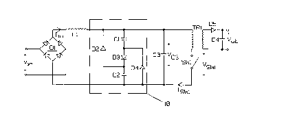
A further embodiment of the present invention is illustrated
in Fig. 4. The arrangement is intended for use in both
European and American electricity supply networks and
delivers essentially the same current to the transformer TR1
in both instances. As with the Fig. 1 embodiment, this
- arrangement includes a rectifier bridge D1 to one output
terminal of which there is connected a first connection
terminal on a first valley-fill circuit 12 via a first
inductor means L2. Similar to the valley-fill circuit 10 in
Fig. 1, the valley-fill circuit 12 includes two capacitors C5
and C6 and three diodes D7, D6 and D8 which correspond
respectively to the first and second capacitor C1 and C2 and
to the first, second and third diodes D3, D2 and D4. There is
connected to the second connection terminal of the first
valley-fill circuit 12 the first connection terminal of a
second valley-fill circuit 14, wherein said second valley-
fill circuit 14 is similar to the first valley-fill circuit
12 and includes two capacitors C7 and C8 and three diodes
D10, D9 and D11 which correspond respectively to the first
and second capacitors C1 and C2 and to the first, second and
third diodes D3, D2 and D4. A second connection terminal on
the second valley-fill circuit 14 is connected to the second
output terminal of the rectifier bridge D1 via a second
inductor means L3. The two inductor means L2 and L3 may be
wound on the same core. A third capacitor C3, which is much
smaller than the capacitors included in the valley-fill
circuits 12, 14 is connected between the first connection
- terminal on the first valley-fill circuit 12 and the second
connection terminal on the second valley-fill circuit 14. A
. 30 loop that includes a primary winding of a transformer TR1 and
a controlled switch means SW1 is coupled in parallel with the
third capacitor C3. Similar to the transformer in Fig. 1, the
CA 02236688 1998-0~-04
W O 97/16884 PCT/SE96/01407
trans~ormer TR1 includes a ~ly-back type converter which also
includes a diode D5 and a capacitor C4. A second switch means
SW2 is also connected between an input terminal on the
rectifier bridge D1 and the interconnection junction between
the first and the second valley-fill circuit 12 and 14
respectively.
The function of the arrangement shown in Fig. 4 will now be
described. The second switch means SW2 is a manually operated
switch which can be caused to change position, or states,
when the arrangement shall be connected to a voltage source
to which it has not earlier been set. When the arrangement is
connected to the European electricity supply network, the
second switch means SW2 is switched-off, whereas the switch
means is switched-on when connected to the American
electricity supply network.
The arrangement functions in the same manner as the
arrangement described with reference to Fig. 1 when the
second switch means SW2 is switched-off, wherein the first
and the second valley-fill circuits 12 and 14 function as a
single valley-fill circuit. All of the capacitors included in
the valley-fill circuits are charged in series, although when
the capacitors discharge the capacitors C8 and C7 in the
second valley-fill circuit 14 discharge in parallel with one
another but in series with the capacitors C5 and C6 in the
first valley-fill circuit 12, these latter capacitors being
discharged in parallel with one another, however. This can be
viewed as though each capacitor in the first valley-fill
circuit forms a capacitive series-circuit together with a
CA 02236688 1998-0~-04
W O 97/16884 PCT/SE96/01407 21
corresponding capacitor in the second valley-fill circuit,
wherein these capacitive series-circuits are discharged in
parallel with one another in the same way as the capacitors
in Fig. 1. When this view is applied to the first described
embodiment, it can be said that the first embodiment included
several capacitive series-circuits but each such capacitive
series-circuit includes only one capacitor.
When the second switch means SW2 is switched-on, the
arrangement operates in a slightly di~ferent manner. For
instance, the first valley-fill circuit 12 is active during
the ~irst half-period and the second valley-~ill circuit 14
is active during the second negative half-period of the
source period. If it is the first valley-fill circuit 12 that
is active in the stationary mode, the second valley-fill
circuit 14 constantly delivers a voltage which is half the
maximum input voltage. Each of the capacitors in the first
valley-fill circuit 12 is charged to a voltage equal to half
the maximum input voltage and when the input voltage reaches
essentially its maximum value, these capacitors are charged
and discharged when the input voltage is at half the maximum
input voltage. There is then applied across the third
capacitor C3 a voltage which varies in the same manner as
that described with reference to Figs. 2 and 3, although the
relationship to the input voltage is different. The voltage
varies between a highest voltage level corresponding to about
1.5 times the peak value of the input voltage and a voltage
which is roughly equal to the peak value of the input
voltage. When the input voltage is above hal~ the maximum
input voltage, the arrangement operates in accordance with
the following step sequenc:
CA 02236688 1998-0~-04
W O 97/16884 PCT/SE96/01407
22
al) When the first switch means SW1 is switched-off, the
third capacitor C3 and possibly the capacitors C5 and C6 in
the ~irst valley-fill circuit 12 is/are charged from the
mains network via the two inductor means L2 and L3.
bl) When the first switch means SWl is then switched-on,
current is supplied to the transformer TRl by the third
capacitor C3 and by said source, via the inductors L2 and L3.
dl) When the voltage across the third capacitor C3 falls to a
voltage which is roughly similar to the voltage across the
capacitors in the first valley-fill circuit 12 plus the
voltage across the capacitors in the second valley-fill
circuit 14, the converter is supplied from the mains network,
via the two inductor means L2 and L3, and also from the third
capacitor C3 and from all capacitors in the two valley-fill
circuits 10 and 12 in the manner described with reference to
this arrangement with regard to discharging of the capacitors
in the two valley-fill circuits when the second switch means
SW2 is switched-off.
When the input voltage is less than half the maximum input
voltage, but greater than zero volt, the transformer TRl is
supplied with current mainly from the capacitors in the two
valley-fill circuits 12, 14.
When the input voltage is beneath O V and beneath half the
minimum input voltage, the arrangement functions in
accordance with the following step sequence:
a2) when the first switch means SWl is switched off, the
third capacitor C3 and possibly the capacitor C7 and C8 in
the second valley-fill circuit 14 is/are charged from the
mains network via the two inductor means L2 and L3,
CA 02236688 1998-0~-04
W O 97116884 PCT/SE96/01407
23
b2) when the first switch means SW1 is then switched-on,
the transformer TR1 is supplied with current by the third
capacitor C3 and said source via the inductor means L2 and
L3; and
d2) when the voltage across the third capacitor C3 falls
to a voltage which is approximately equal to the voltage
across the capacitors in the first valley-fill circuit 12
plus the voltage across the capacitors in the second valley-
fill circuit 14, the converter is supplied ~rom the mains
network, via the two inductors L2 and L3, from the third
capacitor C3 and from the capacitors in the first and the
second valley-fill circuit 10 and 12 in the manner described
for this arrangement with reference to discharging the
capacitors in the two valley-fill circuits when the second
switch means SW2 is switched off.
When the input voltage is below O V and less than half the
minimum input voltage, the transformer TR1 is supplied with
current mainly by the capacitors in the two valley-fill
circuits 12, 14.
The arrangement illustrated in Fig. 4 may, of course, be
modified in the same way as that mentioned with re~erence to
the Fig. 1 arrangement. However, if this embodiment uses HF
ripple filtering capacitors, two capacitors are connected in
series across the output terminals of the rectifier bridge
Dl, wherein the interconnection junction between these two
capacitors is connected to the same input terminal on the
rectifier bridge D1 as that to which the second switch means
SW2 is connected. Furthermore, more than two valley-fill
circuits can be connected between the output terminals of the
rectifier bridge. It will be understood that the invention is
CA 02236688 1998-0~-04
W O 97116884 PCT/SE96/01407
24
not restricted to the use of fly-back type converters, and
that other types of converters may alternatively be used,
such as push-pull converters or forward converters.
A further variant of the Fig. 4 arrangement is one in which
the second switch means SW2 and the leg of the rectifier
bridge connected thereto are excluded, so that the
interconnection junction between the two valley-fill circuits
is connected directly to a pole on the a.c. voltage source.
It will be understood that this latter arrangement is not
restricted to the American electricity supply network.
,