Note: Descriptions are shown in the official language in which they were submitted.
CA 02236830 1998-06-04
-1-
WIDE BANDWIDTH ANTENNA ARRAYS
This invention relates to the radiating elements used in radio
frequency antenna arrays such as are found, for example, in certain
radar equipment and more especially it relates to very wide
frequency bandwidth operation of such antenna arrays.
Electromagnetic energy is radiated from and is 'received by
specially designed antenna structures which can exist in many
topological forms. Very common and simple antenna structures are
seen in applications to automobile broadcast radio reception and
domestic television reception. More complicated antenna structures
c,~n be seen in radar equipment used to detect distant moving
targets for both military and civil purposes.
The most complex radar antennas are examples of a class of
a~:~tenna arrays, employing a plurality of individual small antenna
elements which are interconnected in ways designed to enable, for
e;:ample, electronic steering of the radiated beams of
elect: omagnetic energy in space, without physical movement of they
whole array.
Individual antenna elements forming an array can be, for
ea;ample, simple dipoles which are well known. Such elements are
referred to as fundamental elements and usually have the smallest
possible dimensions for a given frequency of the radiated energy
(Figure 1). The dipole arms la and 1b are usually each one
quarter-wavelength long at the frequency of operation and are
sF~aced one quarter wavelength x above a metallic ground plane 2
to give radiation in the desired direction z. Transmission line 3
CA 02236830 1998-06-04
_2_
supplies energy to the dipo:(e arms la and 1b. The ratio of length. l
to diameter d is usually > 10, which gives satisfactory performance
over a narrow frequency band of a few percent with respect to them
centre frequency of the band. The direction of the electric field
vector is indicated by the arrow E.
Antenna Arrays can be made using a plurality of such
elements, distributed uniformly or non-uniformly over a prescribed
surface area, and chosen to provide the desired antenna radiation.
characteristics. The surface may be planar or curved in more than
one plane and the perimeter may be of any shape, though it is
commonly circular, or rectangular, or simply a straight line, which
is the degenerate case for a rectangular aperture when one side of
the rectangle has zero dimension.
Figure 2 shows a rectangular array of MxN dipole elements S
located over a metallic ground plane 6. Antenna elements in the
array are spaced from each other by locating them on the nodal
points of a geometrical lattice 4, which might be for example either
rectangular (as shown) or triangular in nature. Spacing of the
elements S from each other s, p, and d CallllOt exceed certain
maximum. fractions of the wavelength of the radiated
electromagnetic energy if undesirable features in the array polar
pattern are to be avoided. If this maximum element spacing is
exceeded, in an attempt to rminimise the number of elements in them
array, them "grating lobes" are generated in the polar pattern of the
radiated energy from the array. (rating lobes are replicas of the
:main (fundamental) lobe of the pattern but they are in different
;spatial directions from it.
CA 02236830 2002-05-29
=3-
in radarrapplications it is not possible to distinguish between .
targets detected iri the main beam and in the grating lobe beams
which results in ambiguities. A target detected in a grating lobe
beam will be processed as if it had been received in the main beam
and will be assigned a completely erroneous spatial direction by the
radar signal processor. In radar and in other applications, such as
broadcasting and communications services, grating lobes carry
some of the energy to unwanted spatial regions and so reduce the
operating efficiency of the sys tem.
It is usually possible, for most narrow frequency bandwidth
applications; to accept the array element spacing limitation. If the
main beam of the radiated pattern is not to be electronically
scanned the spacing d in Figure 2 can be up to one half-wavelength
at the operating frequency. If the beam is to be electronically
scanned the spacing must be reduced as the maximum scan angle
increases, down to a maximum of one half wavelength for a scan of
ninety degrees from the normal to the array surface.
However, there are occasions when it is necessary to transmit
and receive electromagnetic energy over a wide frequency range,
for example in frequency agile radars which operate at one or more
frequencies distributed over a prescribed wide frequency range.
Frequency agility can allow the radar or tactical communications
system to continue to operate when interference, of whatever
nature, overwhelms reception on any one frequency. Agility has
other advantages in target detection and signal processing that are
commonly exploited in radar equipment, particularly those applied
to military functions.
CA 02236830 1998-06-04
-4-
It is usually desirable in such frequency agile military
applications to operate over as wide a frequency band as possible:;
at least an octave. This requires that the individual elements of the
array are capable of operating over the chosen frequency range and
that their separations from each other meet the maximum spacing
criterion already described, at all operating frequencies. Clearly
this is not possible with conventional antenna elements such as
single linear dipoles, even though there are established designs for
wide-band dipoles which permit operation over a band-width of
about 30~'% with respect to the mean frequency of the band. For
example, a broad band half wave dipole is described in IEEE
Transactions on Antennas and Propagation, Vol AP-32, No. 4, April
1984 pp 410-412 by M.C. Bailey and describes a bow-tie shaped
dipole, which has a leng th equal to 0.3 2 of the mean wave-length of
the band of operation, and has been shown to have acceptable
performance over a 33% band-width, centred around 600 MHz,
determined on the criterion that the input Voltage Standing Wave
Ratio ( VSWR) shall not exceed 2Ø
Even if it was possible to make a dipole capable of radiating
over an octave change in frequency, it could not satisfy the
separation condition necessary to ensure grating lobe free radiation
over the octave range, from an array formed by a plurality of such
dipoles. The length of the dipole would be between one half-
wavelength at the lowest freduency and one half-wavelength at the
highest frequency, and so the separation between dipoles in the
array must exceed a half-wavelength at the highest frequency if
:physical interference between dipoles is to be avoided.
CA 02236830 1998-06-04
-S-
Mathematical modelling of the bow-tie dipole described in the
previously mentioned article in IEEE Transactions on Antennas and
1'ropagatian, using the proven analysis software Numerical
1?lectromagnetic Code (NEC), has shown that it cannot be designed to
operate over an octave frequency range.
The elements used in an array antenna need not be single
dipoles. A Log-Periodic Dipole Array (LPDA) as shown in Figure 3,
in which a series of half-wavelength dipoles arranged in a coplanar'
and parallel configuration on. a parallel wire transmission line 7,
rnay be used as a very broadband element. The five element LPDA
shown in Figure 3 is representative of the LPDA class of antennas.
The number of dipole elements used in the LPDA depends on the
required performance characteristics. The lengths and spacing of
t:he dipoles in the LPDA increase logarithmically in proportion to
their distance from a fixed co-ordinate reference point 8. Energy is.
fnd to the LPDA from the feed point 9 which is close to the dipole
10, in a direction towards the reference point 8.
The first and last dipoles 10 and 11 respectively are chosen to
suit the frequency band of interest which can be several octaves or
even a decade in extent. Dipole 10 will have dimensions chosen to
make it radiate correctly at the high frequency end of the band. A
metallic ground plane 12 is located approximately one quarter-
wavelength at the lowest operating frequency from dipole 11 to
provide unidirectional radiation which may be desirable in
a~~plications of the invention to radar for example, where energy
radiated in the backward direction may have adverse effects on the
operation of the radar. Transmission line 7 is short circuited by
CA 02236830 1998-06-04
-G-
metallic ground-plane 12 where :it intersects it at point A. Such
LPDA's are well known, for example UK patent no. 884889
describes such an LPDA, and are in wide use. The direction of the
electric field vector radiated or received by the LPDA, known as the
polarisation of the wave, is shown by the arrow E. It lies in the
common plane of the dipolE~s (horizontal as drawn) because the
dipole excitation currents a1.1 lie in that: plane.
A planar array antenna could comprise a plurality of LPDA
elements arranged with the planes containing their individual sets
of dipole:> being normal to t:he planar array. Figure 4 shows
elements 14 -18 in the array, located on the nodal points of
rectangular lattice 19.
A planar array so formed has the advantage that the side-
lobes of the pattern at wide angles from its normal direction are
reduced, compared with the side-lobes from a corresponding array
of single dipole elements, since the beamwidth of the LPDA element
is narrower than that of the dipole element. However, the same
element spacing criterion which applies to the array of the dipole
elements to eliminate grating lobes applies to the array of LPDA
elements, but the grating lobe magnitudes will be reduced by the
narrow beam pattern of the LPDA element.
The LPDA overcomes the frequency bandwidth limitations of
the single dipole element but, just as with the single wide
bandwidth dipole, it fails to :meet the spacing criterion necessary to
suppress grating lobes generated by the planar array. For examplE~,
LPDA's 14 and 15 in Figure 4 cannot be positioned closer in the
array than the longest dipole element, 11 in Figure 3, will allow.
CA 02236830 1998-06-04
-7-
When this is done the high :frequency elements, 20 in LPDA's 14
and 15 will be separated frc>m each other by more than one half-
wavelength at the high frequency; in fact by one wavelength if the
LPDA is designed to operate over an octave, and grating lobes will
be formed at the higher frequencies in the operating band.
An aim of the present invention is to provide a linear array
element which overcomes W a above-mentioned problems.
According to the present inventian, there is provided a linear
antenna array element comprising a plurality of skewed dipoles of
unequal total length and at .least one shorter non-skewed dipole,
said skewed dipoles having their respective poles skewed such that
end sections of said dipoles are of equal length and formed
substantially at an angle to a centre section of said dipole, where
the length of said centre section is substantially equal to the length
of the shortest non-skewed dipole, said poles being connected
alternately to a respective tv~o-conductor transmission line to
ensure correct excitation phases for operation, the conductors being
parallel in the vertical plane and arranged such that the ratio of the
length of .each dipole to its distance from a fixed reference point
located on an axis of said transmission line is constant, and each of
said dipoles has a total length of substantially one half-wavelength
or multiples thereof relating to the desired discrete transmit or
receive frequency within the total band of frequencies.
The end sections are preferably skewed at right angles to the
~~entre section.
CA 02236830 1998-06-04
_$_
According to a further aspect of the invention, each end
section of a respective dipole is positioned in an opposite direction
and lies in a vertical plane.
According to another aspect of the invention, each end section
of a respective dipole points in an opposite direction and lies
substantially in the same horizontal plme.
According to yet another aspect of the invention, each end
section of a respective dipole points in the same direction and lies
substantially in the same horizontal plane.
The present invention removes the restriction on spacing of
the LPDA's in the planar array imposed by the lowest frequency
(longest lE~ngth) dipole in the LPDA, thus permitting acceptable
operation of the planar array antenna over at least an octave
frequency band.
It is evident that skewed LPDA elements may now be ideally
positioned within an array, comprised of a plurality of such
elements, with adjacent elerr.~ent separations which comply with the
grating lolbe suppression criterion, thus allowing the array antenna
beam to be scanned in an ideal way over a frequency band of at
Leas t one oc tave.
A plurality of skewed LPDA elements may be used in arrays
:for particular system applications where wide bandwidth
:frequency agility can provide a useful counter to natural or man-
made interfering signals received by the system.
Various embodiments of the present invention will now be
described with reference to the following drawings, wherein,
CA 02236830 1998-06-04
_.
Figure S shows a skewed Log-Periodic Dipole Array (LPDA), i.n
accordance with the present invention.
Figures 6, 7, 8 and 9 show alternative embodiments of an
LPDA in accordance with the present invention, and
Figure 10 shows a planar array of skewed LPDA's.
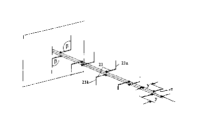
Referring to Figure S, 'there is shown a skewed LPDA in which
the indiv idual dipoles are arranged to be "Z" shaped or skewed, the
angles R between the end segments and the centre segment being
equal to Each other, such that the skewed dipole can be totally
contained within a planar area, where in the case illustrated the
angles R are 90 degrees. More specific~~lly the centre segments of
all of the dipoles are made equal in length and equal to one half-
wavelength at the highest frequency of operation, that is equal in
length (2 times y) to the shortest dipole=_ 10 in a conventional non-
skewed Ll'DA. The two end ;segments 21a and 21b of the 90 degree
skewed dipole 21, for example have equal lengths such that the
total dipole length is the same as its equivalent straight dipole
shown as 13 in Figure 3. Thus the "width" of the LPDA is constant
and is controlled b5~ the highest frequency of operation irrespective
-- of the bar.~dwidth requirement.
An L.PDA formed by a plurality of such skewed dipoles can be
COIlstruCtE'_d in several ways. Figures 6 to 9 show four embodiments
of the invention. It will assist the understanding of the description
to visualise the metallic ground plane as a vertically oriented plane
.and the tvwo-wire transmission line existing in a second vertical
:plane meeting the ground pl;~ne at right angles.
CA 02236830 1998-06-04
-lU-
In Figure 6 the planes containing each of the dipoles that form
t:he LPDA are parallel to each other and parallel to the metallic
ground plane. However, the radiated electric field vector E is now
n.o longer in the horizontal plane since the dipoles forming the
skewed LPI)A have current carrying components (Ih) and (Iv) in
the horizontal and vertical planes respec:tively. The polarisation of
a signal transmitted by the LF'DA is still linear but it is in an
inclined plane, and is the vector addition of the horizontal and
vertical components of the elE~ctric field radiated by the component
parts of them skewed dipoles. It is shown in Figure 6 for the low
frequency dipole arms ??a anal 22b as the components Elh and Elv
and by vector addition the net low frequency field El = Elh+Elv and
it is inclined at angle a to the horizontal where a is given by
t~m-1(Elv~Elh). Clearly a is a maximum for the low frequency
dipole. It is zero for the high frequency dipole since it carries no
vE~rtical current components. Thus the polarisation of the electric
field radiated by the skewed L.PDA is linear and its direction is a
function of frequency. By rec:iprocit<,~ the same statement holds for
signals received by the antenna.
In radar the polarisation of the transmitted signal and hence
th.e polarisation of the received signal is chosen principally through
consideration of the nature of the expected targets and terrain
clutter. It i;; usuall~~ horizontal, vertical, or at 45 degrees.
Depending on the nature of th.e radar and its application, the ability
to operate over a very wide agile bandwidth may override any
disadvantages that may result from polarisation rotation with
frequency. At very high frequencies (VHF) and ultra high
CA 02236830 1998-06-04
-1. l-
frequencies (UHF), there are clear benefits from the diffraction
occurring at the lower frequencies (VHF), when the polarisation is
vertical and foliage penetration properties of the higher
frequencies (UHF), when th.e polarisation is horizontal. These
advantages could be realised from a planar array of a plurality of
the skewed LPDA element illustrated in Figure 6 if the skewed
LPDA is designed to cover the appropriate parts of the VHF and
UHF bands.
A second embodiment of the invention is shown in Figure 7.
Here the skewed dipoles are constrained to a single horizontal
plane, ignoring the small separation of the conductors forming the
feed transmission line 24a and 24b. The linear polarisation of the
electric field transmitted by this embodiment of the skewed LPDA
is therefore horizontal, as might be a specified requirement for a
particular application of the invention, for example higher
frequency radar where the diffraction and foliage penetration
mechanisms are virtually insignificant.
It ha.s been found that 'when the end segments of the dipoles
are skewed such that they are "C" shapE~d and they are arranged in
a parallel and coplanar manner, as shown in Figure 8, the skewed
:LPDA so formed has improved performance at wide angles (a),
'when compared with the performance of the embodiment shown in
;Figure 7. This is because the currents carried by the end segments
of the "C" dipole are equal in magnitude and opposite in direction,
hence the field components radiated by them tend to cancel. When
.x=90 degrees the components exactly cancel and no radiation
CA 02236830 2002-05-29
-I?-
occurs in tha..t direction,_which is ideal for a skewed LPDA element
used in a planar array for radar applications, for example.
A fourth embodiment of the invention is. illustrated in Figure
~ where skewed dipoles of the form illustrated in Figure 8 and the
transmission Line feeding them is etched onto a double sided or two
single sided printed circuit boards 26 as a totally integrated
assembly. This method of construction permits superior control of
manufacturing tolerances and good repeaCability which is an
important advantage at frequencies where the wavelengths are
very small. The dipole elements and transmission Lines may be
contained within a sheet of dielectric material which tapers from a
dimension encompassing the largest skewed dipole to a zero
dimension at a point beyond the shortest and non-skewed dipole.
In each of the embodiments described above, there may be
provided a number of non-skewed dipoles 10 at the end of the
array.
An embodiment of the invention in a planar array of identical
skewed LPDA elements is illustrated in Figure 10. The elements
are positioned on a regular rectangular lattice, having their
respective axes parallel to each other and at right angles to a. plane
forming a basis of said linear array.
A planar array may be constructed of any shape consisting of
a plurality of linear array elements as previously described. The
linear array elements may be located with regular or irregular
separations on nodal points of a lattice. The nodal points may be
rectangular, triangular or any other geometrical shape such that the
CA 02236830 1998-06-04
J_
axes of the linear array elements are parallel to each other and are
at right angles to the plane of the planar array.
A 11011 planar array may be formed by either singly or doubly
curving the surface of the above described planar array.
The application of the invention is not limited to the VHF and
UHF bands and Call 111 principle be used to significant advantage in
any plan~u- or linear array antenna required to operate over wide
bandwidths, particularly an octave or more, for radar,
communications, or other purposes. T:he upper frequency limit is
driven by the accuracy to which the feed point and transmission
line can be constructed.