Note: Descriptions are shown in the official language in which they were submitted.
HYBRID CIRCUIT CONSTRUCTION OF PUSH-PULL POWER AMPLIFIER
BACKGROUND OF THE INVENTION
Technical Field
This invention relates to circuit structures having an integrated circuit flip
mounted on a base substrate having metalization connected to the integrated
circuit. More specifically, it relates to such an integrated circuit having a
plurality of
devices, with interconnection between the devices being provided by
metalization
on the substrate.
Back4round Art
Because GaAs integrated circuits are comparatively expensive, it is common
to make microwave and millimeter (mm) wave circuits as hybrid circuits. The
active
devices that require the use of GaAs are fabricated on GaAs chips which are
then
mounted on a motherboard having a less expensive substrate, such as silicon,
AI203, BeO, and AIN.
Conventional circuits having a plurality of active devices are made by
fabricating a separate integrated circuit or chip for each of the active
devices.
Circuit metalization and passive devices are printed on the motherboard and
each
chip is then mounted at an assigned site on the motherboard. The integrated
circuit
on the chip can be very simple, such as a single FET. It may also be more
complex,
incorporating a variety of devices to provide an overall function, such as is
provided
by an amplifier.
A complex circuit may require that numerous such chips be made and
mounted. The resultant requirement for individual handling of small chips also
tends to make the fabrication process somewhat costly. Alternatively, when a
chip
has a complex circuit, it is more expensive to make since it requires a larger
GaAs
substrate than its more simple cousin, and the benefits of hybrid circuit
structure are
not as fully realized.
There is thus a need for a method of hybrid circuit construction, and thereby
a hybrid circuit structure that, when applied to microwave and mm-wave
circuits,
minimizes the size of GaAs substrates used and is simple to fabricate, thereby
providing for efficient fabrication at reduced cost.
CA 02236993 2000-03-06
CA 02236993 1998-05-07
WO 97/17755 PCT/US96/17358
DISCLOSURE OF INVENTION
These features are provided in the present invention by an improved hybrid
circuit and a method for making it. A chip is constructed which has a
plurality of
electrical devices and a plurality of associated terminals disposed at
selected
locations on a common face of the chip, there being at least one terminal for
each
device. Correspondingly, a circuit is constructed on a base substrate,
referred to as
a subcircuit of the overall hybrid circuit, which has a plurality of terminals
on a
common face of the base substrate corresponding in location to the terminals
on the
chip. The chip is mounted on the subcircuit with the terminals of the chip
mounted
to the corresponding terminals of the subcircuit. The electrical devices are
thereby
connected to respective terminals of the subcircuit.
The chip is preferably cut from a wafer containing a large array of devices.
The chip then may consist of a smaller array of adjacent devices, which
devices may
be identical or different. The subcircuit terminals are thus also laid out in
a
corresponding array for interconnecting the chip terminals.
In one preferred form the present invention provides a means of connecting a
plurality of essentially identical active devices for the purpose of
multifunction
(multiple functions) and multiple function (multiples of a function)
operation. These
devices are mounted on a chip which in turn is flip-mounted onto a motherboard
circuit having passive elements. If these passive devices were on the chip,
the size
of the expensive active medium would be increased, greatly increasing the
overall
cost. This is due to the fact that the active areas are typically much smaller
than the
passive areas.
This invention can be used in making many different kinds of circuits, such as
amplifiers, oscillators, detectors, mixers, and other circuits using a
plurality of
identical or different active devices, preferably using a single active-device
matrix
chip.
As a specific example, a push-pull power R.F. amplifier made according to
the invention comprises a first pair of active devices, such as field-effect
transistors
(FETs), having respective control terminals (gates) and current-carrying
terminals ,
(drains and sources). One of the current-carrying terminals of each of the
active
2
-3-
devices is coupled to a reference potential, such as a circuit or virtual
ground. An
input electromagnetic coupler, such as a transformer or balun, has an input
primary conductor electrically coupled between the input terminal and the
control
terminal of a first one of the pair of active devices. An input secondary
conductor
is electromagnetically coupled to the input primary conductor and electrically
coupled between an input reference potential and the control terminal of a
second
one of the pair of active devices.
An output electromagnetic coupler has a primary conductor
electrically coupled between the other of the current-carrying terminals of
the first
active device and the output terminal. An output secondary conductor is
electromagnetically coupled to the output primary conductor and is
electrically
coupled between the other of the current-carrying terminals of the second
active
device and the reference potential of the output primary conductor.
As a result, the signal on the output terminal is a combination of the
signals being conducted by the pair of active devices. The pair of active
devices
may be formed on a single chip having separate terminals connected to the
active
devices which are flip-mounted onto corresponding terminals on a substrate on
which the transformers or baluns are formed. The input and output transformers
or
baluns may also be formed as slotlines or coplanar waveguides on the
substrate.
The slotlines may be U-shaped with a first portion extending adjacent to a
second
portion, the first portion providing electromagnetic coupling to a signal
transmitted
along the second portion. The first and second portions are defined by a
peninsula conductor extending into the U-shaped slotline. The chip is mounted
relative to the substrate with the control terminal of one of the active
devices flip-
mounted on the
CA 02236993 2000-03-06
-3a-
peninsula conductor. One embodiment provides a conversion from a slotline to a
coplanar waveguide by the use of a circular opening at the end of the U-shaped
slot. These openings function as open circuits, thereby allowing the input
signal to
be carried by respective signal conductors formed as an open-ended conductor
leg extending into the U-shaped slot.
According to the invention, there is provided a push-pull power
amplifier for amplifying an input radio frequency signal, comprising: an input
terminal for receiving an input radio-frequency signal; an output terminal for
outputting an amplified radio-frequency signal; an integrated circuit chip
having a
first pair of active devices, the chip having a control terminal and at least
one
current-carrying terminal associated with each active device, the currents
flowing
through the current-carrying terminals depending upon the signals applied to
the
control terminals; a substrate having a plurality of terminals, the chip being
mounted with each chip terminal flip mounted onto a corresponding substrate
terminal; an input electromagnetic coupling means formed on the substrate and
having an input primary conductor electrically coupled between the input
terminal
and the substrate terminal corresponding to the control terminal of a first
one of
the pair of active devices, and an input secondary conductor
electromagnetically
coupled to the input primary conductor and electrically coupled between an
input
reference potential and the substrate terminal corresponding to the control
terminal of a second one of the pair of active devices; and an output
electromagnetic coupling means also formed on the substrate and having a
primary conductor electrically coupled between the substrate terminal
corresponding to one of the current-carrying terminals of the first active
device
and
CA 02236993 2000-03-06
-3b-
the output terminal, and an output secondary conductor mutually
electromagnetically coupled to the output primary conductor and electrically
coupled between the substrate terminal corresponding to one of the current-
carrying terminals of the second active device and an output reference
potential;
the signal on the output terminal being a combination of the signals being
conducted by the pair of active devices.
It will thus be apparent that the present invention provides a circuit
which is simple and economical to construct. These and other features and
advantages of
CA 02236993 2000-03-06
CA 02236993 1998-OS-07
WO 97/17755 PCT/US96/17358
the present invention will be apparent from the preferred embodiments
described in
the following detailed description and illustrated in the accompanying
drawings.
BRIEF DESCRIPTION OF DRAWINGS .
FIG. 1 is a simplified plan view of a portion of a wafer having an array of
FETs for use in making a circuit according to the invention. .
FIG. 2 is a schematic of a push-pull amplifier circuit that can be made
according to the invention using a set of FETs from the array of FIG. 1.
FIG. 3 is a schematic of multiple series-connected circuits of FIG. 2 using a
chip having an extended array of FETs.
FIG. 4 is a simplified plan view of a chip usable in the circuits of FIG. 3.
FIG. 5 illustrates a plan view of a first embodiment of the circuit of FIG. 3
using microstrip-line conductors.
FIG. 6 illustrates a simple schematic of a push-pull amplifier usable in a
second embodiment of the invention.
FIG. 7 illustrates a plan view of the second embodiment of the circuit of FIG.
3 using slotlines.
FIG. 8 illustrates a plan view of the layout of FETs in an array usable as a
chip for the embodiment of FIG. 7.
FIG. 9 illustrates a plan view of a third embodiment of the circuit of FIG. 3
using coplanar waveguides.
FIG. 10 is an enlarged view illustrating the FET layout for a chip in the
circuit
of FIG. 9.
FIG. 11 is a plan view illustrating yet a fourth embodiment of the circuit of
FIG. 3 having a conversion of slotline to dual coplanar waveguide.
BEST MODE FOR CARRYING OUT THE INVENTION
One aspect of the present invention is directed to the use of a single chip
having a plurality of active devices separately connected to a subcircuit
formed on a
motherboard. Referring initially to FIG. 1, an array 10 of active devices,
shown as
FETs 12, are formed on a wafer 14 using conventional techniques. The term
active ,
4
CA 02236993 1998-OS-07
WO 97/17755 PCTlUS96/I7358
device refers to individual elements, such as transistors, or to any related
integrated
circuit, such as an amplifier.
Vertical and horizontal dashed lines, such as lines 16 and 18, illustrate
potential saw or scribe streets for dividing one or more sets of FETs from
adjacent
FETs. Each FET includes a gate 20, or control terminal, a source 22 and a
drain
24. The source and drain are also referred to as current-carrying terminals.
Each
gate, source and drain is connected to at least one connection terminal, such
as
respective terminals 26, 28 and 30.
Wafers 14 may be produced in large volumes, thereby making each active
device relatively inexpensive. Selected wafers may then be divided into arrays
of
active devices by dividing them using a selected cut pattern so that the
resulting
chips have active devices with connection terminals corresponding in position
to
connection terminals on a motherboard. By changing the wafer cut pattern
different
arrays of active devices can be used to form different circuits. In one
application of
this concept, the active devices on a chip are not interconnected. In other
applications, however, there may be some interconnection, while still having
separate connection terminals for each active device. An example of this
latter
feature is shown in FIGs. 9 and 10, described below, in which adjacent like
terminals, such as sources or drains, are connected together.
FIG. 1 illustrates a simple form of the invention in which all of the devices
on
the wafer are identical. When it is desired to use different devices, a wafer
is made
with clusters of the different devices in a repeated configuration or pattern.
One application where individual, multiple-device arrays may be used is in
the construction of a gate array of large transistors for high current
conduction or
high power output. For microwave and mm-wave applications, this is often
provided
by the connection of FETs by Wilkinson combiners or the equivalent to provide
impedance transformation as well as to combine multiple terminal connections.
Similar results may be achieved using a push-pull amplifier circuit, such as
b
circuit 32 shown in FIG. 2. This circuit, while providing inherent benefits,
particularly
with respect to impedance transformation, over conventional multi-FET,
parallel
connected power amplifiers, may be constructed using an active-device array
chip
5
CA 02236993 1998-OS-07
WO 97/17755 PCT/LTS96/17358
as has been described with reference to FIG. 1. Circuit 32 includes an input
terminal 33, an input electromagnetic coupling 34 formed by a first input
coupling
element 35 and a second input coupling element 36 electromagnetically coupled
to
element 35.
A chip 38, represented by dashed lines, includes first and second FETs 39
and 40. Element 35 couples the input terminal to the gate of the first FET.
Element
36 couples the gate of the second FET to a common potential, such as ground.
The drain of FET 39 is coupled to an output terminal 42 by a first output
coupling element 44 forming part of an output electromagnetic coupling 45. A
second output coupling element 46, electromagnetically coupled with element
44,
couples the drain of FET 40 to ground.
Through electromagnetic coupling on the input and output, the signal is
divided for amplification by two FETs. This structure may be used in a
series/parallel push-pull configuration, as shown in FIG. 3 for impedance
transformation. This figure illustrates a power amplifier 50 having a
plurality of
series (push-pull) sections, such as sections 52 and 54. Each section 52 and
54
includes two circuit portions 56 and 58 that are equivalent to circuit 32 of
FIG. 2
except that rather than the connections to ground, the two circuit portions
are joined
together, as shown at connections 60 and 62. This results in a virtual ground
at the
point of connection.
By dividing an input signal into a signal for each circuit section and
recombining the output signals, such as by the use of Wilkinson dividers,
substantial
power combination is achieved. Impedance matching can be provided at the
individual FETs, or before or after signal division or recombination.
The FETs may be aligned in a linear array 64 of FETs, which array may be
formed of a single chip 66 fabricated as has been described with reference to
FIG.
1. An exemplary FET or bipolar transistor physical diagram for chip 66 is
shown in
FIG. 4. In this case, the transistors are shown as replications of transistor
pairs Q~
and Q 2, Q 3 and Q 4, and the like. Each transistor pair corresponds with the
first
and second FETs in a circuit portion shown in FIG. 3. As was described with
reference to FIG. 1, each FET, such as FET Q~, includes a gate 68, a gate
terminal
6
CA 02236993 1998-OS-07
WO 97117755 PCT/US96/I7358
69, a source 70, a source terminal 71, a drain 72, and a drain terminal 73.
The
structures of these transistor pairs can be different, depending on the
respective
functions they perform.
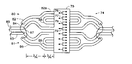
A first embodiment of power amplifier 50 is shown as amplifier 74 in FIG. 5.
Chip 75 has eight FETs, including FETs 76, 77, 78 and 79. Amplifier 74
includes
similar series push-pull circuit sections 80 and 81. Quarter-wave input
microstrip-
line conductors 82 and 83 are connected by an air bridge 84. Similarly, input
microstrip-line conductors 85 and 86 are connected by an air bridge 87. These
conductors, which include quarter-wave portions such as portiori 82a, provide
input
signals to each section. Electromagnetic coupling provides a complementary
input
signal to the second FET of the lower portion of each section, such as FETs 77
and
78. The respective second FETs are coupled together by respective U-shaped
conductors 88 and 89. The microstrip lines on the output side are similar in
general
form to the conductors on the input side.
The microstrip lines are designed to achieve whatever impedance is needed.
The input or output impedances are connected in series until the impedance is
high
enough, and then they are connected in a number of parallel sections
appropriate
for the desired power level.
FIGs. 6-8 illustrate a power amplifier 90 that embodies the invention using
slotlines. FIG. 6 is a schematic of a push-pull section 92 having two FETs 91
and
93 with joined sources. Two balanced input signals are applied to the
respective
gates, and two balanced output signals are produced on the respective drains.
FIG. 7 illustrates the preferred form of the slotlines for section 92 and an
additional section 95 similar to section 92, as they would appear on the
substrate of
a motherboard, on a hybrid substrate, or on another type of base substrate.
Amplifier 90 is operationally equivalent to amplifier 76. An input slotline
94, also
referred to as a subcircuit of the circuit of amplifier 90 and formed by
opposite
planar conductors 96 and 98, is shaped like a reverse "E" with a long center
leg
portion 94a, oppositely extending transverse bends 94b and 94c, and closed-
ended
outer leg portions 94d and 94e that are parallel to center leg portion 94a.
This
.,
shape produces respective open-ended conductor fingers 96a and 98a extending
7
between the slotline leg portions.
The outer leg portions function as RF chokes. The output slotline 100 is a
mirror image of the input slotline and functions the same way although the
dimensions will be different due to impedance-matching differences of the
input and
output circuits. Corresponding FET structure is shown by chip 102 in FIG. 8 as
it
would appear when mounted on slotlines 94 and 100. Chip 102 contains FETs 91,
93, 104 and 106, having respective gate, source and drain terminals identified
as G,
S, and D. These terminals line up with the corresponding terminals identified
in
FIG. 7.
Chip 102 is flip mounted onto the metalization shown in FIG. 7, with the gate
connected to the ends of the input fingers, the source is connected to a
conductor
108 connecting conductors 96 and 98 between the backs of the E-shaped
slotlines.
Conductor 108 functions as a virtual ground. The drain terminals are
accordingly.
connected to the ends of the output fingers, as shown.
FIGs. 9 and 10 illustrate yet a third power amplifier 110 embodying the
invention. FIG. 9 illustrates a subcircuit 112 formed as metalization on the
substrate
of a motherboard, and FIG. 10 is an enlarged view of a flip-mounted chip 114
as it
appears when mounted on the metalization. As is described in U.S.
patent 5,613,231 assigned
to the same assignee as the present invention, coplanar waveguides also
provide
impedance matching and signal transmission for power amplifiers.
Metalization 112 includes an input coplanar waveguide 116 having a signal
conductor 118 and opposing planar ground or reference conductors 120 and 122.
The signal conductor is initially a single line 118a, and then divides at a
junction 124
into dual lines 118b and 118c. A resistor 126 connects lines 118b and 118c. A
ground conductor 128 extends between the signal line.
Except for impedance-matching differences, an output coplanar waveguide
130 is substantially a mirror image of the input coplanar waveguide relative
to a
connecting ground plane strip 132 extending under FET-array chip 114. This
metalization results in the array of FETs being connected in parallel rather
than in
serieslparallel for push-pull operation, although the metalization for push-
pull could
8
CA 02236993 2000-03-06
CA 02236993 1998-OS-07
WO 97/I7755 PCT/US96/I7358
also readily be constructed.
FIG. 10 is an illustration of FET chip 114 having two sets 134 and 135 of
double FET-pairs 136. Each FET-pair 136 in the chip has an associated terminal
flip-mounted to corresponding terminals on the subcircuit. Thus, a gate
terminal 138
is connected to gates 139 and 140. Source terminals 141 and 142, and drain
terminal 143, are connected respectively to sources 144 and 145, and drain
146.
FET terminals 138, 141, 142 and 143 are connected to respective subcircuit
terminals 150, 151, 152 and 153.
Drain 146 functions as a dual drain for both FETs in each FET-pair 136.
Similarly, each source like source 142 serves as a source for associated FETs
in
adjacent pairs. These double-duty terminals thus are, in effect, connected
terminals.
Although chip 114 is specially designed in this embodiment, it could be
modified to be cut from a wafer of sets of FET-pairs. In such a case, separate
source terminals would be provided for each FET-pair 136 or set of double FET-
pairs. Alternatively, amplifier 110 could be made with parallel, dual
metalizations
112 and 130 to which is mounted a single chip having the FET configuration of
chip
114 duplicated.
Finally, FIG. 11 illustrates a portion of a power amplifier 160 having a
motherboard subcircuit 162 to which is flip-mounted a FET chip 164, shown in
dashed lines. As was the case with amplifier 110, the FETs, such as FET 166,
in
the array 168 of FETs in chip 164, are connected electrically in series at the
input
(gate).
The input portion of subcircuit 162 is different in this embodiment. It
provides
a conversion from an input slotline 170, formed by coplanar conductors 172 and
174, to dual coplanar waveguides 176 and 178. These output lines could be
combined in a manner similar to the input circuit or as push-pull lines.
Instead of
terminating in the E-shaped slot of amplifier 90 illustrated in FIG. 7, a slot
180
divides at a junction 182 into elongate U-shaped slots 180a and 180b.
The U-shaped slots terminate in circular openings 180c and 180d. These
openings function as open circuits, thereby allowing the input signal to be
carried by
9
CA 02236993 1998-OS-07
WO 97/17755 PCT/US96/17358
respective conductors formed as open-ended conductor legs 172a and 174a
extending into the U-shaped slots. An intermediate conductor 184, connected to
conductors 172 and 174 beneath chip 164, extends from junction 182 to source
terminals, such as terminal 186, of the FETs. The mounting and connection of
the
FETs to the conductors is the same as that described with regard to amplifier
90.
INDUSTRIAL APPLICABILITY
It will therefore be appreciated that the present invention provides a hybrid
circuit structure in which a plurality of active devices are formed,
preferably in an
array, on a chip that is mounted on, and individually connected to a
subcircuit
formed on the substrate of a motherboard. This invention is particularly
useful for
multifunction chips and power amplifiers, although it is applicable to any
circuit or
combination of circuits requiring contact with a plurality of individual
active devices.
The present invention is also particularly useful for push-pull configurations
of FETs,
for which various coplanar metalization patterns provide particular benefit.
Connections may also exist between the active devices on a chip, and the
subcircuits to which each active device is connected do not have to be
related.
Other examples of circuits which would be advantageously embodied
according to the invention include a power amplifier with an internal
detector, a
receiver with an RF low noise amplifier, a mixer, such as a Gilbert cell
mixer, an
oscillator with or without a tunable varactor, and an intermediate frequency
amplifier. The invention is also applicable to phase shifters, particularly
distributed
line (artificial transmission line) types.
Preferably, in all these cases, the matrix die or chip only has active
devices,
such as FETs, that are flip-mounted to a substrate. Several advantages are
thereby
realized. The chip may be made using a single, simple FET process, as well as
a
MMIC process. Prototyping is easily accommodated since the wafer can be cut up
into a variety of different configurations. The production units can then be
made the
same as the prototype. Suitable wafers can be made even before the application
is
determined. High yields and high volume production are realizable.
It will therefore be apparent to one skilled in the art that variations in
form and
CA 02236993 1998-OS-07
WO 97/I7755 PCTli7S96/I7358
detail may be made in the preferred embodiments without varying from the
spirit and
scope of the invention as defined in the claims and any modification of the
claim
language or meaning as may be provided under the doctrine of equivalents. The
- preferred embodiments are thus provided for purposes of explanation and
illustration, but not limitation.
11