Note: Descriptions are shown in the official language in which they were submitted.
CA 02237460 1998-0~-13
ADAPTIVE MULTIPLE SUB-BAND COMMON-MODE RFI SUPPRESSION
FIELD OF THE INVENTION
This invention relates to a method and apparatus for reduçing in~ r~irt;nce in
5 communications channels and is especially, but not exclusively, applicable to the
suppression of common mode noise, including radio frequency inte,relence, in digital
subscriber loops of telephone systems.
BACKGROUND OF THE INVENTION
A balanced digital subscriber loop comprising a twisted wire pair carries both
dirr~lt;.~lial and common mode currents induced by the signal and noise sources,respectively. In a perfectly balanced loop, the common mode currents will not interfere
with the dirrer~ntial current (information signal). However, when bridge taps, poorly
twisted cable, and so on, cause the circuit to be unbalanced, longitu~lin~l current injected
by extemal noise sources will be converted into differential current at the receiver and
detected as noise. Such noise can lead to errors by introducing jitter in timing extraction
circuits or by causing false pulse detection. In digital loops, common mode noise can be
conveniently categorized into the following: Impulse noise, Radio Frequency Inlelreleilce
(RFI) and Crosstalk Noise. With the trend towards higher bit rates in the loops, radio
intelrelence, typically caused by radio stations in the vicinity and hence tr~n.~mitting on
certain frequencies with a relatively narrow bandwidth, is assuming greater ~i~nific~nce.
When telephone subscriber loops operated at relatively low frequencies, perhaps
3,000 Hz. or 4,000 Hz., interference could be dealt with adequately by using twisted wire
cable, which helps to cancel out any induced intelrel~ilce, and by means of hybrid
2 5 transformers. With the introduction of VDSL (Very high speed Digital Subscriber Loops)
and ADSL (Asymmetric Digital Subscriber Loops), the frequency of operation is
approaching the radio frequency bands and the aforementioned balancing of the cable is no
longer sufficient to reduce the inte.releilce. As a result, common mode noise increases.
Various techniques, other than such balancing, are known for reducing inlelÇerence
or noise in a communication channel. For example, U.S. patent number 5,555,277,
discloses a technique for c~ncelling common mode switching noise to achieve reduced error
rates in a local area network. This technique involves gain controllers at both tr~n~mitter
CA 02237460 1998-0~-13
and receiver ends to mailllain signal integrity during tr~nsmic~ion. In addition, noise
cancellation at the receiver is p~lÇollned by generating primary and inverted copies of the
received signal, amplifying both primary and inverted signals, and then summin~ them to
cancel the induced common mode noise. This technique is not entirely satisfactory because
5 it addresses common mode noise within the transceiver but not common mode noise in the
tr~n~mis~i~ n ch~nnel itself.
To mitig~te common mode noise on a pair of signal conductors, the system disclosed
in US patent number 3,705,365 issued Dec. 5, 1972 uses a two conductor shielded cable,
a three-winding transformer, and a bipolar differential amplifier. The common mode signal
10 from the cable shield is used to cancel the common mode noise using the third winding in
the transformer. This technique is not entirely suitable for twisted wire tr~n~mi~sion lines,
such as telephone subscriber loops.
U.S. patent number 4,283,604 discloses an electronic hybrid in the form of a current
source circuit with common mode noise rejection for a two-wire tr~n~mi~sion system. The
15 circuit provides an electronic int~rf~ce for coupling signals with a tr~n~mi~ion line and
opeldtes to cancel or negate the effect of unwanted impedance on the line, thereby
improving common mode impedance across the pair and enhancing the common mode
rejection to noise ratio in the two-wire system. Like a conventional hybrid transformer, this
electronic hybrid will not operate ~ti.sf~ctorily when the line is not balanced, especially
2 o when the line is a relatively long telephone subscriber loop.
Eulo~l patent application number 0 453 213 A2 discloses a radio receiver in
which an adaptive notch filt~ring approach is used to reduce intelrelc;nce in a radio
frequency received signal carrying digital data at 2.4 kilobits per second using a 3 to 30
MHz r.f. carrier. The adaptive notch filter is implemented using frequency domain analysis
25 of quantized data to detect inl~lr~l~nce by comr~ring the received signal frequency
spectrum with a known spectrum template. Any frequency band with higher power than
the reference template is considered to have inlelrelt;nce. A programmable notch filter is
then tuned to nullify the signal power in the respective freguency band. Unfortunately, the
received signal in the selected band is cancelled along with the inlelrelence, res~llting in an
30 undesirable loss of signal information. A further disadvantage is that the technique also
re~uires the intelrerence rejection filter to be trained, which entails the tr~nsmission of a
CA 02237460 1998-0~-13
training sequence periodically belween tr~n~mi~ions of the data stream, thus reducing
overall tr~n~mi~ion efficiency.
Hence, none of these various techniques con~titutes a satisfactory way of reducing
common mode noise in subscriber loops opel~ling at the proposed very high speed levels
s of VDSL or ADSL. In TlEl.4/96-084 dated April 18, 1996, and at a VDSL workshop at
IEEE Globecom, November 18, 1996 in London, England, John Cioffi and John Bingham
proposed doing so by me~ ring the voltage between ground and the centre tap of the usual
hybrid transformer at the end of the subscriber loop and extracting a signal representing
common mode noise. Cioffi et al. proposed to filter this common mode noise signal using
an adaptive wide band filter to provide a radio frequency noise estim~te and subtract it from
a differential signal obtained from the secondary of the hybrid transformer to produce an
error signal for tuning the adaptive filter to reduce that error signal to zero. The circuit can
only tune the filter when there are quiet periods in the received signal. This is not entirely
satisfactory because it involves timing to ensure that the quiet periods are detected. Re~use
noise patterns may change, the filter must be tuned frequently, which increases overhead,
reducing the efficiency of the tr~n~mi~sion. Also, the adaptive filter has to have a
bandwidth at least as wide as the bandwidth of the received signal which, in the case of
VDSL, might be from zero to about 10Mz. Such a filter would be complex and expensive
to make. Moreover, the arrangement might not work in places where a proper ground
cannot be located, such as a rocky region.
An object of the present invention is to elimin~te or at least miti~te the
disadvantages of the foregoing known techniques and provide a noise suppression
arrangement that is better adapted to the reduction of common mode noise in two-conductor
communications ch~nnels, such as twisted wire subscriber loops.
SUMMARY OF THE INVENTION
According to one aspect of the present invention, noise suppression appa~dllls for a
two-conductor communications channel comprises:
(i) a hybrid device connected to the channel for providing a differential mode signal
corresponding to a differential signal received from the channel,
(ii) a device for extracting from the channel a corresponding common mode signal,
CA 02237460 1998-0~-13
(iii) a noise estim~tion unit responsive to the common mode signal and a frequency
control signal for deriving from the common mode signal a noise estim~te signal
representing a common mode noise level in a selected frequency band having a bandwidth
considerably narrower than an ope~aling bandwidth of said differential signal,
s (iv) means for providing a noise-~u~pr~ssed output signal as the difference between the
differential mode signal and the noise estim~te signal; and
(v) noise detection and control means responsive to said common mode signal for
detecting within the opel~ling bandwidth a narrow frequency band wherein instant noise
level is higher than in other parts of the operating bandwidth, such narrow frequency band
having a bandwidth significantly less than an opel~ting bandwidth of said differential signal,
and generating said frequency control signal for adjusting said noise estim~tion means so
that said selected frequency band corresponds to that of the instant highest noise signal.
The noise estim~tion unit may comprise means responsive to a second control signal
for adjusting the noise estim~tion signal so as to correspond to the differential mode noise
in the differential mode signal, and the noise detection and control means may further
comprise means responsive to the common mode signal and the noise-suppressed output
signal for generating said second control signal in dependence upon a colllpalison between
the common mode signal and the noise-suppressed output signal when the noise estimation
means is set to the selected frequency band.
In colllpaling the common mode signal and the noise-suppressed output signal, the
means for generating the second control signal preferably p~lrOlllls cross-correlation
between the common mode signal and the noise-corrected signal to determine whether or
not the noise estim~tion signal has subst~nti~lly cancelled the differential noise in the output
signal.
In prefelled embodiments of the invention, the noise estim~tion unit comprises aplurality of tunable nallowl,and bandpass filter units, the noise detection and control means
provides a plurality of frequency control signals, each for a different one of the tunable
narrowband bandpass filter units, each filter unit is responsive to a respective said frequency
control signal to supply a respective one of a plurality of components of said noise
3 o estim~tion signal, and the noise detection and control unit is arranged to scan said operating
bandwidth a plurality of times and, after each scan, adjust a different one of the frequency
CA 02237460 1998-0~-13
control signals to adjust the corresponding one of the filter units to the noisiest band
detected during that scan.
According to a second aspect of the invention, noise suppression apparatus for a two-
conductor communications channel comprises:
5 (i) a hybrid device connected to the channel for providing a differential mode signal
corresponding to a differential signal received from the channel,
(ii) a device for extracting from the channel a co"espoading common mode signal,(iii) a noise estim~tion unit comprising a plurality of noise estim~tion means for deriving
a col,esl?ol ding plurality of noise estim~te col"ponent signals for respective ones of a
lo plurality of selected frequency bands, each noise estim~tion means being responsive to the
common mode signal and a corresponding one of a plurality of frequency control signals
for deriving from the common mode signal a noise estim~te signal component representing
a common mode noise level in a sel~cted frequency band having a bandwidth considerably
na"ower than an ope,~ting bandwidth of said differential signal,
15 (iv) means for ~umming the noise estim~tP signal components to provide a noise estimate
slgnal;
(v) means for providing a noise-~upplessed output signal as the difference between the
differential mode signal and the noise estim~te signal; and
(vi) noise detection and control means responsive to said common mode signal for20 sc~nning the operating bandwidth a plurality of times to detect, for each scan, that narrow
frequency band wherein instant noise level is higher than in other parts of the operating
bandwidth, each such narrow frequency band having a bandwidth ~i&nifi~ntly less than an
operating bandwidth of said differential signal, and generating for each scan one of said
frequency control signals for adjusting the co~sponding one of said noise estim~tion means
25 so that the corresponding said selected frequency band corresponds to that of the instant
highest noise signal.
According to a third aspect of the invention, a method of suppressing noise in asignal received from a two-conductor communications channel comprises the steps of:
(i) using a hybrid device connected to the channel to provide a differential mode signal
30 co~les~nding to a dirre,~nlial signal received from the channel,
(ii) extracting from the channel a corresponding common mode signal,
CA 02237460 1998-0~-13
(iii) responsive to the common mode signal and a fre~uency control signal, deriving from
the common mode signal a noise estim~te signal representing a common mode noise level
in a selected frequency band having a bandwidth considerably narrower than an operating
bandwidth of said diffelential signal,
5 (iv) providing a noise-~u~ssed output signal as the difference between the differential
mode signal and the noise estim~te signal; and
(v) responsive to said common mode signal, detecting within the operating bandwidth
a narrow frequency band wherein instant noise level is higher than in other parts of the
operating bandwidth, such narrow frequency band having a bandwidth significantly less than
lo an opel~ting bandwidth of said differential signal, and generating said frequency control
signal for adjusting said selected frequency band to collt;sl)ond to that of the instant highest
noise signal.
According to a fourth aspect of the invention, a method of suppressing noise in a
signal received from a two-conductor communications channel comprises the steps of:
5 (i) using a hybrid device connected to the channel, a differential mode signal colrti~llding to a differential signal received from the channel,
(ii) extracting from the ch~nnel a cG~sponding common mode signal,
(iii) responsive to the common mode signal and each of a plurality of frequency control
signals, deriving a plurality of noise estim~te signal col-lponents each representing a
20 common mode noise level in a selected frequency band having a bandwidth considerably
nallower than an operating bandwidth of said differential signal,
(iv) sllmming the noise estim~te signal components to provide a noise estim~te signal;
(v) providing a noise-suppressed output signal as the difference between the differential
mode signal and the noise estim~te signal; and
2 5 (vi) sc~nning the common mode signal over the operating bandwidth a plurality of times
and detecting, for each scan, that narrow frequency band wherein instant noise level is
higher than in other parts of the operating bandwidth, each such narrow frequency band
having a bandwidth .si~nifi~ntly less than an ope.dting bandwidth of said differential signal,
and generating for each scan one of said frequency control signals for adjusting the
3 o corresponding said selected frequency band to co~les~nd to that of the instant highest noise
signal.
CA 02237460 1998-0~-13
BRIEF DESCRIPTION OF THE DRAWINGS
Embodiments of the invention will now be described by way of example only and
with reference to the accoll.panying drawings in which:-
Figure 1 is a schematic diagram of a two-wire communications channel showing thepaths of common mode and differential mode culle~ and the introduction of radio
frequency intelfe~ence or noise from an RF radiation source;
Figure 2 is a simplified schematic block diagram of a noise suppression circuit
according to the present invention and comprising a noise detection and control unit and a
noise estim~tion unit;
Figure 3 is a block schematic diagram of the circuit of Figure 2 but showing thenoise estim~tion unit in more detail;
Figure 4 is a schematic block diagram of the circuit of Figure 2 but showing thenoise detection and control unit in more detail; and
Figure 5 illustrates a second embodiment suitable for implementation using a digital
signal processor.
DETAILED DESCRIPTION OF PREFERRED EMBODIMENTS
In the drawings, identical or corresponding colllponents in the different Figures have
the same reference numbers.
Referring to Figure 1, a transmitter 10 is shown connected to one end of a twisted
pair subscriber loop 11 by way of a hybrid or balance transformer 12. A similar
transformer 13 connects the far end of the loop 11 to a receiver 14. Injection of radio
frequency noise into the subscriber loop 11 is represented by an RF source 15 feeding an
~ntenn~ 16 which couples radio frequency signals, as noise, into the subscriber loop 11.
The injected noise signals are injected as common mode signals but are converted into
dirrelelltial mode current at the receiver 14 and detected as noise.
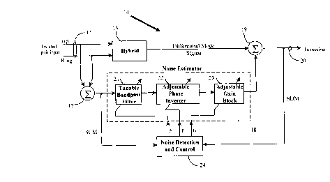
Referring to Figure 2, in a receiver 14 according to a first embodiment of the
invention, the TIP and RING of the twisted wire subscriber loop 11 are connected to
respective inputs of a hybrid circuit 13. The signal at the input of hybrid 13 comprises a
differential signal coupled with the common mode signal. The common mode signal is
extracted from the twisted wire pair 11 by a summer 17, respective inputs of which also are
connected to the TIP and RING of the subscriber loop 11. The output of the summer 17
CA 02237460 1998-0~-13
is connected to a noise estim~tor circuit 18 which produces noise estim~te signal that is
subst~nti~lly phase-inverted and supplies it to one input of a second summer 19. The other
input of summer 19 is connected to the output of hybrid 13. The second summer 19 adds
the differential mode signal extracted by the hybrid 13 to the "inverted" noise estim~te
signal, thereby subtracting common mode noise from the differential mode signal, and
supplies the resulting signal to an output port 20 for supply to the receiver 14 (not shown
in Figure 2). The differential mode signal output from summer 19 will be improved in that
it will have a higher Signal to Noise Ratio (SNR).
Common mode noise is estim~t~d by adding the in-phase TIP signal and anti-phase
RING signal in a twisted pair cable with respect to ground reference. It should be noted
that the common mode signals in both the TIP wire and the RING wires are in phase with
each other. Therefore, the common mode signal is extracted while the differential mode
signal is cancelled out when the TIP and RING signals are added at summer 17. The
extracted common mode signal from s~lmmer 17 is then processed by the noise estim~tor
18.
Within the noise estim~tor 18, the common mode signal is filtered in adjustable
bandpass filter bank 21 and phase-inverted by adjustable phase inverter unit 22. The
resulting signal is scaled by an adjustable gain unit 23 which compensates for signal loss
in the adjustable phase inverter 22 and other co...ponents in or precetiin~ the noise estim~tQr
20 18. The output of the adjustable gain unit 23 is the phase-inverted noise estimate signal
which is combined with the differential mode output of hybrid 13.
The respective output signals from the summer 17 and the s--mmer 19 also are
supplied to a noise detection and control circuit 24 which uses them to derive control signals
for controlling the tunable bandpass filter bank 21, adjustable phase inverter unit 22 and
25 adjustable gain unit 23.
The noise detection and control unit 24 performs spectral analysis upon the common
mode signal to locate narrowband noise signals and adjusts the centre frequencies of the
individual bandpass filters in bandpass filter bank 21 to coincide substantially with the
centre frequencies of the nal,owl,alld noise signals. The control unit 24 also controls the
3 o amount of phase shift provided by adjustable phase inverter 22. The phase inverter 22 will
not necessarily provide exactly 180 degrees of phase shift but rather, to compensate for the
nonlinear phase delays inherent in hybrid 13, and the summer 17 and filter bank 21, will
CA 02237460 1998-0~-13
provide sufficient phase shift for the noise estim~tion signal to be substantially 180 degrees
out of phase relative to the differential mode noise in the differential mode signal at the
summer 19.
The control unit 24 also controls the adjustable gain unit 23 so as adjust the
amplitude of the noise estim~t~ signal to the appropliate level to cancel the differential mode
noise in the differential mode signal.
Typically, the controller 24 can be implemented by a low speed microcontroller
because the real-time requirement to pelro~"- the above adaptive computations is low.
The noise estim~tor 18 will now be described in more detail with reference to Figure
0 3. The noise estim~tor 18 comprises several identical channels. The number of channels
depends upon the number of n~lowl~alld common mode noise bands that need to be
suppressed. To simplify the description, however, only three channels are shown,design~ted A, B and C. Identical components in the three channels have the same reference
numbers but with the channel identifier as a suffix.
The three channels comprise tunable nallowl,alld bandpass filters 21A, 21B and 21C,
respectively, each having a bandwidth of, for example, 100 kHz. The centre frequency of
each bandpass filter can be adjusted to match the centre frequency of narrowband noise
detected by p~lror,.lil~g spectral analysis of the common mode signal in the adaptive
controller 24, as will be discussed in more detail later. As a result, the output signals from
2 o each of the bandpass filters 21A, 21B and 21C will each be a narrowband component of the
common mode noise.
Each of the bandpass filters 21A, 21B and 21C has its output connected to the input
of a respective one of three adjustable phase shifters 22A, 22B and 22C. Differential mode
and common mode signals propagate dirrelel,lly in the twisted wire pair 11 and the hybrid
13. The phase relationship between the two propagation modes is not constant with respect
to frequency; rather the difference in phase between the two propagation modes increases
with frequency. Beyond a few megahertz, multiple periods of phase delay are exhibited
between the common mode and differential mode. Therefore, the adjustable phase shifters
22A, 22B and 22C must be capable of re~ ning the common mode signal to the
differential mode noise in the dirrerenlial mode signal such that there is a 180 phase
dirrerence between the signals in the frequency bandwidth of the corresponding noise
suppression channel A, B or C.
CA 02237460 1998-0~-13
Each of the phase shifters 22A, 22B and 22C has its output connected to the input
of a respective one of three amplifiers 23A, 23B and 23C, respectively, which constitute
the adjustable gain unit 23. The amplitude of the differential mode noise is dependent on
the loop balance, more particularly dependent upon the amount of common mode noise
5 which couples via the hybrid 13 into the differential mode signal. Therefore, the common
mode signal is scaled to match the amplitude of the differential noise by adaptively
controlling the gain of the adjustable gain units 23A, 23B and 23C. It should be noted that
better cable, such as data grade cable, exhibits better noise immunity, so a smaller portion
of the common mode noise will couple into the differential mode path.
The phase-inverted and scaled common mode noise estimate signals from the
amplifiers 23A, 23B and 23C, respectively, are combined by a third summer 25 and the
res~llting combined phase-inverted common mode noise estimate signal supplied, as the
output of noise estim~tor 18, to the summer 19, which adds the combined phase-inverted
common mode noise estim~te signal to the differential mode signal containing the "common
15 mode" residual noise, thereby effecting suppression of the residual noise.
The noise detection and control unit 24 will now be described in more detail with
reference to Figure 4. Briefly, the control unit 24 detects the residual noise at the output
port 20 to modify adaptively the parameters of each of the channels A, B and C of the
multichannel noise estim~tor 18 to minimi7e the noise at output port 20. Such noise
20 detection involves computing the average of the cross-correlation between the differential
and common mode signals, as will be discussed later.
Spectral analysis of the common mode signal so as to estim~te residual noise in the
differential mode signal could be performed simply by computing a Fourier transform of
the common mode signal, but such an approach requires intensive computations and thus
2 5 a high speed processor. To avoid the need for a high speed processor, spectral analysis is
accomplished by sweeping a narrowband bandpass filter 29 incrementally throughout the
entire frequency band of the digital subscriber loop 11, i.e. the bandwidth of the transmitted
signal spectrum. As shown in Figure 4, first bandpass filter 29 has its input connected to
the output of summer 17 to receive the common mode signal (SCM). Second bandpass3 o filter 44 has its input connected to the output of summer 19 to receive the noise-corrected
differential mode signal (SDM). A control signal for causing the filter 29 to sweep the
required frequency band are supplied by a microcontroller 30, the digital output of which
CA 02237460 1998-0~-13
is converted to an analog control signal by a digital-to-analog converter 31. The analog
signal from D-to-A converter 31 is supplied to the filter 29 by way of multiplexer 32 and
one at a set of sample-and-hold circuits 33.
The common mode noise signal comprises a p~b~nd signal which is converted into
a baseband signal by demod~ ting it with a carrier signal from a voltage controlled
oscillator 34. Thus, the common mode signal from the output of first passband filter 29 is
amplified by variable-gain amplifier 35 and supplied to a multiplier 36 which mixes it with
the signal from the VCO 34. The rçsulting signal is filtered by low pass filter 37 to extract
the baseband signal which then is converted to a digital signal by analog-to-digital converter
o 38 at the input to microcontroller 30. The frequency of VCO 34 is controlled by the
microcontroller 30 by way of D-to-A converter 31, multiplexer 32 and a sample-and-hold
circuit 39. The microcontroller 30 adjusts the frequency of VCO 34 so that the common
mode signal will fit into the frequency range of the A-to-D converter 38.
When the system is first switched on, the microcontroller 30 will cause the common
mode signal (SCM) passband filter 29 to scan the entire frequency range of signal received
from the subscriber the loop 11. The microcontroller 30 will record the centre frequency
of the narrowband having the largest amplitude and generate a control signal, as described
before, to adjust the first bandpass filter 21A in the noise estim~tor 18 to set it to the same
centre frequency.
After a suitable interval has elapsed to allow for the bandpass filter 21A, phase
shifter 22A and amplifier 23A to "settle", the microcontroller 30 performs cross-correlation
between the common mode signal SCM and the differential mode signal SDM to determine
whether or not the gain of amplier 23A needs to be adjusted. As mentioned previously,
there may be losses in the hybrid 13 and in the various components of the noise estim~t--r
18. Consequently, the amplitude of the common mode noise estim~te signal from channel
A may be greater, or less than that required for cancellation of the residual noise in the
differential mode signal.
The cross-correlation is performed while the bandpass filter 21A and 29 set to
substantially the same centre frequency.
3 o The microcontroller 30 provides further control signals by way of D-to-A converter
31, multiplexer 32, and sample-and-hold circuits 33 to increment the frequency of tunable
filter 29 in steps which are equal to the passband of the tunable filters 21A, 21B, and 21C
CA 02237460 1998-0~-13
in the noise estim~tion unit 18, i.e. in steps of 100 Khz. At each 100 Khz interval, the
microcontroller 30 measures and stores in memory the power level of the received signal.
When the microcontroller 30 has completely scanned the entire frequency range, it selects
the highest power value recorded and then, by way of D-to-A converter 31, multiplexer 32
5 and the a~ro~liate one of three sample-and-hold circuits 49, sets the first tunable bandpass
filter 21A in the noise estim~tion unit 18 to the centre frequency of that narrowband.
While the first bandpass filter 21A was being set to the highest noise band, thedifferential mode signal path was free running. Once the first tunable filter 21A has been
set or locked to its noise narrowband, and begins to suppress the noise in that band, the
10 noise component in the differential mode signal is reduced. In the noise detection and
control unit 24, this differential mode signal is passed through second bandpass filter 44,
amplifier 45 and multiplier 46 in the SDM path (Figure 4). The multiplier 46 will pt;lro~
cross-correlation by multiplying the common mode signal (SCM) by the differential mode
signal (SDM), producing a residual signal which is rather noisy. A low pass filter 47
15 connects to the output of multiplier 46 and removes high frequency components or
harmonics from the residual signal. A sliding average integrator 48 then extracts the DC
component from the filtered signal and applies it to the A-to-D converter 38. Amplifier 45
simply adjusts the amplitude of the signal from filter 44 to a suitable level for processing
by the A-to-D converter 38. The microcontroller 30 determines whether the residue tracks
2 o the noise and whether its amplitude is positive or negative, indicating that the amplitude of
the differential mode signal noise component is smaller or greater than the common mode
noise component extracted from TIP and RING via summer 17. By way of D-to-A
converter 31, multiplexer 32 and sample-and-hold circuits 49, the microcontroller 30 adjusts
the phase shifter 22A and amplifier 23A in channel A of the multi-channel noise estimator
25 18, both to correct phase differences between the signals and to adjust amplitude. The
adjustment of phase and gain will continue until the residual signal is substantially zero.
At this point, the first filter channel A is correctly set to the first noisy narrow band.
Thus, radio frequency inlelrelence (RFI) is detected by sweeping the entire
frequency band of the common mode signal while differential mode noise is detected by
3 o sweeping the cross-correlation between differential and common mode signals.The microcontroller 30 then repeats the process, looking for the next noisiest narrow
band. Hence, the microcontroller 30 scans tunable filter 29 to detect the second-noisiest
CA 02237460 1998-0~-13
narrow band and sets the second tunable filter channel components 21B, 22B and 23B to
the second noisiest band. It should be noted that, at this time, the first tunable filter
channel A will have s~pressed the first noisiest band, so the microcontroller 30 will again
look for the noisiest narrow band in the u~ ing range at that time. Again, once the filter
5 22B has been set to the centre fre~uency of the second noisy band, the microcontroller 30
pelrolllls cross-correlation to adjust the phase and gain in channel B so as to reduce the
residual differential noise mode substantially to zero.
The process is repeated once more to set the third channel C to the third-noisiest
band, at which point all of the tunable filter ch~nnel~ A, B and C will have been set to
10 respective noisy bands selected in descending order of noise power.
Assuming an operating fre~uency range from zero to 10 MHz, and tunable filters
21A, 21B and 21C having bandwidth of 100 kHz bandwidth, it is expected that perhaps
three tunable filters will be sufficient for most applications involving subscriber loops using
twisted wire pairs. This recognises that the nature of common mode noise in these systems
15 tends to be concentrated in certain bands, perhaps because it is inl~lrelence from a
neighbouring radio station. Nevertheless, it will be appreciated that a greater number of
bandpass filters could be used if desired.
It would be possible to implement both the noise estim~tor 18 and the noise detection
and control unit 24 digitally, pell,a~s using a digital signal processor. As illustrated in
20 Figure 5, in order to permit such a digital implementation, the signals into and out of the
noise estim~tor 18 and noise detection and control unit 24 would need to be converted.
Thus, a first analog-to-digital converter 50 is inserted at the output of summer 17, and a
second analog-to-digital converter 51 between the output of summer 19 and the SDM input
of noise detection and control unit 24. A digital-to-analog converter 52 and low pass filter
25 53 are inserted between the output of the noise estimator 18 and the corresponding input of
summer 19. When implementing the noise detection and control unit 24 digitally, a Fast
Fourier Transform process will be used to produce the control signals for noise estimator
18. More particularly, the bandpass filters 21A, 21B and 21C would be combined and the
necessary coefficients loaded into them periodically. When the noise estimator 18 is
30 implemented digitally, it is also possible for the microcontroller 30 to adjust the bandwidth
of each of the filters 21A, 21B and 21C to approximate more closely the bandwidth of the
corresponding narrowband noise signal. The detailed implementation of the digital noise
CA 02237460 1998-0~-13
estim~tor and digital noise detection and control unit will not be described in detail since
the substitution of digital counlelpall~ for the analog sample-and hold components, VCO,
analog filters, multipliers and so on would be obvious to a person skilled in this art.
In many cases, the RFI will be at fixed fre4uencies, perhaps because it is from a
5 local AM radio station. In such a case, the bandpass filter(s) could be tuned manually
following inst~ tion, rather than adaptively as described hereinbefore.
Embodiments of the invention permit dominant common mode noise such as RFI to
be reduced significantly. The noise reduction in a twisted-pair cable will improve the
Signal-to-Noise ratio, thereby increasing the reach of digital subscriber loop modems or
lo allowing higher sign~lling rates in the same cable.