Language selection

Search

Patent 2237505 Summary

Third-party information liability

Some of the information on this Web page has been provided by external sources. The Government of Canada is not responsible for the accuracy, reliability or currency of the information supplied by external sources. Users wishing to rely upon this information should consult directly with the source of the information. Content provided by external sources is not subject to official languages, privacy and accessibility requirements.

Claims and Abstract availability

Any discrepancies in the text and image of the Claims and Abstract are due to differing posting times. Text of the Claims and Abstract are posted:

  • At the time the application is open to public inspection;
  • At the time of issue of the patent (grant).
(12) Patent: (11) CA 2237505
(54) English Title: MOS IMAGE SENSOR
(54) French Title: CAPTEUR D'IMAGES A DISPOSITIFS MOS
Status: Deemed expired
Bibliographic Data
(51) International Patent Classification (IPC):
  • H01L 27/14 (2006.01)
  • H01L 27/146 (2006.01)
  • H04N 5/335 (2011.01)
  • H04N 3/15 (2006.01)
(72) Inventors :
  • ACKLAND, BRYAN DAVID (United States of America)
  • INGLIS, DAVID ANDREW (United States of America)
  • LOINAZ, MARC J. (United States of America)
(73) Owners :
  • LUCENT TECHNOLOGIES INC. (United States of America)
(71) Applicants :
  • LUCENT TECHNOLOGIES INC. (United States of America)
(74) Agent: KIRBY EADES GALE BAKER
(74) Associate agent:
(45) Issued: 2002-01-22
(22) Filed Date: 1998-05-13
(41) Open to Public Inspection: 1998-12-20
Examination requested: 1998-05-13
Availability of licence: N/A
(25) Language of filing: English

Patent Cooperation Treaty (PCT): No

(30) Application Priority Data:
Application No. Country/Territory Date
08/879,926 United States of America 1997-06-20

Abstracts

English Abstract


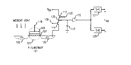
An image sensor circuit which employs a photodiode in conjunction with a charge
transfer mechanism. By employing the photodiode, at least a portion of the light sensed
does not pass through a layer of polysilicon, and so is not prevented from reaching the
sensing area by the polysilicon. The image sensor circuit of the invention is made up of
device structures readily available in standard CMOS process technologies
Advantageously, image sensors embodying the invention show substantially improved
quantum efficiency for short wavelength light over the prior art sensors. In addition,
image sensors embodying the invention display improved dark current uniformity, thus
improving yield.


French Abstract

L'invention est un circuit capteur d'images qui utilise une photodiode conjointement avec un mécanisme de transfert de charges. En utilisant une photodiode, au moins une partie de la lumière détectée ne traverse pas une couche de polysilicium et, par conséquent, n'est pas empêchée d'atteindre la zone de détection par le polysilicium. Le circuit de l'invention est constitué de structures facilement disponibles sous la forme de dispositifs CMOS standard. Dans la concrétisation privilégiée de l'invention, les capteurs d'images ont un rendement quantique substantiellement amélioré aux courtes longueurs d'onde par rapport aux capteurs actuels. De plus, ils ont une plus grande uniformité quant au courant d'obscurité, ce qui accroît le rendement.

Claims

Note: Claims are shown in the official language in which they were submitted.


What is claimed is:

1. An image sensor circuit, comprising:
a first photodiode, having first and second terminals;
a first metal oxide semiconductor (MOS) transistor, a drain of said MOS transistor
being coupled to said first terminal of said first photodiode for collecting charge
developed by light falling on said first photodiode;
a second MOS transistor, a source of said second MOS transistor being coupled tosaid first terminal of said first photodiode and to said drain of said first MOS transistor;
a capacitor, one terminal of said capacitor being coupled to a drain of said second
transistor;
a third MOS transistor, said source of said third MOS transistor being coupled to
said drain of said second transistor;
wherein said charge collected in said first MOS transistor is transferred through
said second MOS transistor and converted into a voltage by said capacitor.

2. The invention as defined in claim 1 wherein charge transference occurs when asignal is applied to a gate of said first MOS transistor so as to turn said first MOS
transistor off.

3. The invention as defined in claim 1 wherein charge transference occurs when asignal is applied to a gate of said first MOS transistor is driven so as to substantially
eliminate its inversion layer.

4. The invention as defined in claim 1 wherein said second MOS transistor is
configured as a common gate transistor.

5. The invention as defined in claim 1 wherein said sensor is reset by applying a
signal to turn said third MOS transistor on.

6. The invention as defined in claim 1 wherein said circuit is manufactured on ap-substrate and said first terminal of said first photodiode is a cathode of said first
photodiode.


7. The invention as defined in claim 1 wherein said circuit is manufactured on an
n-substrate and said first terminal of said first photodiode is an anode of said first
photodiode.

8. The invention as defined in claim 1 wherein said third MOS transistor is a
PMOS transistor and wherein said connections of said drain and said source of said third
MOS transistor are reversed.

9. The invention as defined in claim 1 wherein said insulator layer is an oxide
layer.

10. The invention as defined in claim 1 wherein said insulator layer includes
silicon dioxide.

11. The invention as defined in claim 1 further including a second photodiode
having a first of its terminals coupled to a source of said first MOS transistor and wherein
said first MOS transistor also collects charge developed by light falling on said second
photodiode.

12. The invention as defined in claim 11 wherein said circuit is manufactured ona p-substrate and said first terminal of said second photodiode is a cathode of said second
photodiode.

13. The invention as defined in claim 11 wherein said circuit is manufactured onan n-substrate and said first terminal of said second photodiode is an anode of said second
photodiode.

14. The invention as defined in claim 1 wherein said capacitor is coupled to an
amplifier.

15. The invention as defined in claim 14 wherein said amplifier is coupled to a
sample-and-hold circuit.

16. The invention as defined in claim 14 wherein said amplifier is coupled to atleast two sample-and-hold circuits.


17. The invention as defined in claim 16 wherein said third MOS transistor is
turned on and a representation of a first output is stored in a first of said at least two
sample-and-hold circuits while said first MOS transistor is enabled to turn on by a signal
applied to a gate of said first MOS transistor.

18. The invention as defined in claim 16 wherein said third MOS transistor is
turned off and a representation of a second output is stored in a second of said at least two
sample-and-hold circuits while said first MOS transistor is turned off by a signal applied
to a gate of said first MOS transistor.

19. The invention as defined in claim 16 wherein said third MOS transistor is
turned off and a representation of a second output is stored in a second of said at least two
sample-and-hold circuits after said first MOS transistor is turned off by a signal applied
to a gate of said first MOS transistor.

20. The invention as defined in claim 16 wherein said third MOS transistor is
turned on and a representation of said first output: is stored in a first of said at least two
sample-and-hold circuits while said first MOS transistor is enabled to turned on by a
signal applied to a gate of said first MOS transistor and thereafter said third MOS
transistor is turned off and a representation of said second output is stored in a second of
said at least two sample-and-hold circuits after said charge accumulated by said first
MOS transistor is transferred to said capacitor by a signal applied to a gate of said first
MOS transistor.

21. The invention as defined in claim 20 further including means for determininga difference between said representation of said first output is stored in said first of said at
least two sample-and-hold circuits and said representation of said second output is stored
in said second of said at least two sample-and-hold circuits

22. An image sensor circuit, comprising:
a p-substrate having formed therein at least one n+ region, a junction between said
p-substrate and said n+ region forming a first photodiode;
an insulator layer between said p-substrate layer and a layer of polysilicon to form
a first NMOS transistor, a cathode of said at least one photodiode being coupled to a
drain of said NMOS transistor, said first NMOS transistor being for collecting charge
developed by light falling on said first photodiode;


a second NMOS transistor, a source of said second NMOS transistor being
coupled to said first terminal of said first photodiode and to said drain of said first NMOS
transistor;
a capacitor, one terminal of said capacitor being coupled to a drain of said second
transistor;
a third MOS transistor, said source of said third MOS transistor being coupled to
said drain of said second NMOS transistor;
wherein said charge collected in said first NMOS transistor is transferred through
said second NMOS transistor and converted into a voltage by said capacitor.

23. The invention as defined in 22 wherein said third MOS transistor is a NMOS
transistor.

24. The invention as defined in 22 wherein said third MOS transistor is a PMOS
transistor.

25. The invention as defined in 22 further including at least a second n+ region, a
junction between said p-substrate and said second n+ region forming a second
photodiode, a cathode of said second photodiode being coupled to a source of said first
NMOS transistor wherein said first NMOS transistor also collects charge developed by
light falling on said second photodiode.

26. The invention as defined in claim 22 wherein said insulator layer is an oxide
layer.

27. The invention as defined in claim 22 wherein said insulator layer includes
silicon dioxide.

28. An image sensor circuit, comprising:
a n-substrate having formed therein at least one p+ region, a junction between said
n-substrate and said p+ region forming a first photodiode;
an insulator layer between said n-substrate layer and a layer of polysilicon to form
a first PMOS transistor, an anode of said photodiode being coupled to a drain of said
PMOS transistor;


a second PMOS transistor, a source of said second PMOS transistor being coupled
to said first terminal of said first photodiode and to said drain of said first PMOS
transistor;
a capacitor, one terminal of said capacitor being coupled to a drain of said second
transistor;
a third MOS transistor, said source of said third MOS transistor being coupled to
said drain of said second PMOS transistor;
wherein said charge collected in said first PMOS transistor is transferred through
said second PMOS transistor and converted into a voltage by said capacitor.

29. The invention as defined in claim 28 wherein said third MOS transistor is anPMOS transistor.

30. The invention as defined in claim 28 wherein said third MOS transistor is anNMOS transistor.

31. The invention as defined in claim 28 further including at least a second p+
region, a junction between said n-substrate and said second p+ region forming a second
photodiode, an anode of said second photodiode being coupled to a source of said first
PMOS transistor wherein said first PMOS transistor also collects charge developed by
light falling on said second photodiode.

32. The invention as defined in claim 28 wherein said insulator layer is an oxide
layer.

33. The invention as defined in claim 28 wherein said insulator layer includes
silicon dioxide.

34. A method for operating an image sensor circuit, said image sensor including
a first photodiode, having first and second terminals;
a first metal oxide semiconductor (MOS) transistor, a drain of said MOS transistor
being coupled to said first terminal of said first photodiode for collecting charge
developed by light falling on said first photodiode;
a second MOS transistor in a common gate configuration, a source of said second
MOS transistor being coupled to said first terminal of said first photodiode and to said
drain of said first MOS transistor;


a capacitor, one terminal of said capacitor being coupled to a drain of said second
transistor;
a third MOS transistor, said source of said third MOS transistor being coupled to
said drain of said second transistor;
the method comprising the steps of:
collecting electrons developed by light falling on said first photodiode;
setting the value of a voltage across said capacitor to a first value;
storing a representation of said first value;
transferring said collected electrons to said capacitor; and
storing a representation of the value of a second voltage across said capacitor after
said transferring step.

35. The invention as defined in claim 34 further including the step of developing
a difference between said stored representation of said first value and said stored
representation of the value of a second voltage across said capacitor after said transferring
step.

Description

Note: Descriptions are shown in the official language in which they were submitted.


CA 02237~0~ 1998-0~-13


MOS IMAGE SE'NSOR

Techn;cal Field
s This invention relates to CMOS active pixel sensors, and more particularly, to
photodiode-based CMOS active pixel sensors.

Background of the Invention
A ~vell known problem in the art of photogate CMOS and CCD image sensors is
that of recluced short wavelength optical response. More specifically, one photogate
0 circuit disclosed in United States PaLtent No. 5,576,763, issued to Ackland, et al. on Nov.
19, 1996 achieves very low read noise. As disclosed, the main photosensitive region of
the photogate circuit is the depletion region under the photogate and the region that is
within the minority carrier diffusion length of the edge of that depletion region. The
photogate is made large in area so as to maximize the number of collected electrons.
However, the photogate sensor circuit suffers from poor quantum efficiency for short
wavelength light due to the absorption characteristics of the polysilicon gate material
employed. This problem is aggravated by the use of silicided gates which are used in
many current CMOS fabrication processes. Photogate CCD image sensors, e.g. frametransfer CC'D's, also suffer from this problem.
Photodiode-based image sensors have a better short wavelength optical response
properties. However, CMOS photodiode-based image sensors suffer from a problem
with reset noise. Specifically, it is impractical to save the actual reset value for the
sensor, which is subtracted from the sensor output to elimin~te the effect of reset noise
from the sensor output. Therefore, a simulated reset value for a sensing cycle is
2s developed using the output of the sensor after it is reset for the next sensing cycle.
However, such simulated reset values may not accurately represent the actual reset value
for the sensing cycle in which they are used, resulting in a poorer image quality.

Summary of the Invention
The problems with prior image sensors are ameliorated, in accordance with the
principles of the invention, by an image sensor circuit which employs a photodiode in
conjunction with a charge transfer me~h~ni~m in lieu of the prior art photogate light
sensor. By employing the photodiode, at least a portion of the light sensed does not pass
through a liayer of polysilicon, and so is not prevented from reaching the sensing area by
the polysilicon The image sensor ciircuit of the invention is made up of device structures

CA 02237~0~ 1998-0~-13


s readily available in standard CMOS process technologies Advantageously, image sensors
embodying the invention show substantially improved quantum efficiency for shortwavelength light over the prior art sensors. In addition, image sensors embodying the
invention display improved dark current uniforrnity, thus improving yield. Further
advantageously, image sensors of the present invention have lower reset noise than prior
10 art CMOS photodiode image sensors.

Brief Description of the Drawing
In the drawing:
FIG. 1 shows an exemplary embodiment of an image sensor circuit which
employs a photodiode in conjunction with a charge transfer mechanism and is compatible
s with CMOS manufacturing processes, in accordance with the principles of the invention;
FIGs. 2-5 show various possible arrangements for laying out the sensor on a
silicon integrated circuit; and
FIG. 6 shows a circuit schematic representation of the sensor

Detailed Description
FIG. 1 shows an exemplary embodiment of an image sensor circuit which
employs a photodiode in conjunction with a charge transfer mechanism and is compatible
with CMOS manufacturing processes, in accordance with the principles of the invention.
The image sensor circuit shown in FIG. 1 includes p-substrate 101, n+ regions
103 and 10 5, silicon dioxide (SiO2) layer 107, polysilicon layer 109, transistors l l 1 and
25 l 13, amplifier 1 15, and parasitic capacitor 1 17. The boundary of n+ region 105 with p-
substrate 101 forms photodiode D1 while the boundary of n+ region 103 with p-substrate
101 forms photodiode D2. Polysilicon layer 109, SiO2 layer 107, and p-substrate 101
form a gate, which need not be a photogate, of NMOS transistor 121 which is formed by
n+ region 103, n+ region 105, p-substrate 101, SiO2 layer 107, and polysilicon layer 109.
Operation of the circuit shown in FIG. l is as follows. The light to be sensed falls
on photodiodes D1 or D2. In such photodiodes, the photosensitive regions comprise the
depletion region and the region that is within one minority carrier diffusion length of the
edge of thalt depletion region. D2, along with D1, form photosensitive regions that have
high quantum efficiency in the short wavelength region of the visible spectrum.
3s Gate terminal 119 oftransistor 121 is held high, allowing incident light to produce
electron-ho]e pairs in the depletion region underneath photodiodes D1 and D2 and gate
SiO2 layer 107. The generated electrons are collected and stored lm~lemeath the gate for
a period of time, e g., 30 milliseconds. During this time, electrons from n+ region 103

CA 02237~0~ 1998-0~-13


will occupy most of the interface states in the interface formed by p-substrate 101 and
SiO2 layer 107 underneath the gate of transistor 121. This results in a reduced thermal
carrier generation and hence reduced dark current. Furthermore, the reduced dark current
results in a higher pixel yield.
At the end of the collection time period, in order to read out the sensor, terminal
o 123 of transistor 113 is pulsed high momenta~ily, in order to reset the voltage at node
125. The reset value seen at the output of amplifier 115 is stored by sample-and-hold
circuit 127. Gate terminal 119 of transistor 121 is then forced low momentarily, causing
the charge stored under gate SiO2 laLyer 107 to be transferred to node 125. This occurs by
operation of transistor 111 as a common gate amplifier. To this end, gate terminal 139 of
transistor 111 is biased to a substantially fixed voltage, such as in the range of 0-3 volts,
e.g., 1 volt
The transferred charge is stored in parasitic capacitor 117, which converts the
charge into a voltage. Parasitic capacitor 117 is small in comparison to the total
capacitance of diodes Dl, D2 and transistor 121. Advantageously, when the charge is
20 transferred to parasitic capacitor, a larger voltage change is developed than if parasitic
capacitor 117 had the same capacitaLnce value as the total capacitance of diodes Dl, D2
and transistor 121. This voltage "gain" reduces the effect of random noise in the readout
circuits, which include amplifier l l S and all circuits subsequent to the output thereof.
The voltage developed at node 125 is then amplified by amplifier 115, and the
25 amplified voltage is stored in a second sample-and-hold circuit 129. The difference
between the outputs of sample-and-hold circuits 127 and 129, Vsig, is the output of the
circuit. This output difference is an example of correlated double sampling, by which,
advantageously, in this instance, a) the effects of reset noise, b) the effects of threshold
voltage vaIiations in transistor 113, c) offset variations in amplifier 115, and d) switching
30 feedthroug:h in transistor 113 during the reset operation are canceled by the difference
operation.
FICrs. 2-5 show various possible arrangements for laying out the sensor on a
silicon integrated circuit. The legend for the various layers that implement the sensor are
shown in each of the FIGs. Elements having the sarne number as an element in FIG. 1
35 correspond to the same element. In FIGs. 2-5 amplifier 115 has been implemented by
transistor 235 and a selection control transistor 237 has been added to selectively address
the output of the sensor. Note that n+ region 105 can be merged into n+ region 103 to
form a sin~;le photodiode region, as shown in FIGs. 3 and 5.

CA 02237~0~ 1998-0~-13


s For convenience, FIG. 6 shows a circuit schematic representation of the sensor.
Again, elernents having the same mlmber as an element in FIG. l correspond to the same
element.
It is noted that amplifier 115 serves to isolate capacitor 117 from the line
capacitance and the capacitance of sample and hold circuits 127 and 129.
o Those of ordinary skill in the art will readily recognize how to implement the
invention using PMOS bransistors and/or p+ to n photodiodes. It will also be recognized
that any insulating material may be used in lieu of silicon dioxide.
Note that only one photodiode need be employed. If so, the diode employed will
be D1 forrned by the junction of n-~ region 105 (FIG. I) and p-substrate 101. If such a
circuit is e mployed, transistor 121 although seeming to lack a source, because of the
absence of n+ region 103, can still be thought of a transistor with its drain and source
short circuited. In any event, the charge collection and transfer operation will be the same
as describe d above.
Although transistor 113 has been shown as an NMOS transistor, it will be
recognized that a PMOS transistor can give an improved reset, as it can pull the voltage at
the drain of the transistor higher than a corresponding NMOS bransistor can pull its
source.
The foregoing merely illusbates the principles of the inventions. It will thus be
appreciated that those skilled in the art will be able to devise various arrangements which,
although not explicitly described or shown herein, embody the principles of the invention
and are included within its spirit ancl scope.


Representative Drawing
A single figure which represents the drawing illustrating the invention.
Administrative Status

For a clearer understanding of the status of the application/patent presented on this page, the site Disclaimer , as well as the definitions for Patent , Administrative Status , Maintenance Fee  and Payment History  should be consulted.

Administrative Status

Title Date
Forecasted Issue Date 2002-01-22
(22) Filed 1998-05-13
Examination Requested 1998-05-13
(41) Open to Public Inspection 1998-12-20
(45) Issued 2002-01-22
Deemed Expired 2017-05-15

Abandonment History

There is no abandonment history.

Payment History

Fee Type Anniversary Year Due Date Amount Paid Paid Date
Request for Examination $400.00 1998-05-13
Registration of a document - section 124 $100.00 1998-05-13
Application Fee $300.00 1998-05-13
Maintenance Fee - Application - New Act 2 2000-05-15 $100.00 2000-03-29
Maintenance Fee - Application - New Act 3 2001-05-14 $100.00 2001-03-23
Final Fee $300.00 2001-10-19
Maintenance Fee - Patent - New Act 4 2002-05-13 $100.00 2002-04-24
Maintenance Fee - Patent - New Act 5 2003-05-13 $150.00 2003-05-01
Maintenance Fee - Patent - New Act 6 2004-05-13 $200.00 2004-05-11
Maintenance Fee - Patent - New Act 7 2005-05-13 $200.00 2005-04-25
Maintenance Fee - Patent - New Act 8 2006-05-15 $200.00 2006-04-24
Maintenance Fee - Patent - New Act 9 2007-05-14 $200.00 2007-04-23
Maintenance Fee - Patent - New Act 10 2008-05-13 $250.00 2008-04-22
Maintenance Fee - Patent - New Act 11 2009-05-13 $250.00 2009-04-30
Maintenance Fee - Patent - New Act 12 2010-05-13 $250.00 2010-04-29
Maintenance Fee - Patent - New Act 13 2011-05-13 $250.00 2011-04-28
Maintenance Fee - Patent - New Act 14 2012-05-14 $250.00 2012-04-17
Maintenance Fee - Patent - New Act 15 2013-05-13 $450.00 2013-04-10
Maintenance Fee - Patent - New Act 16 2014-05-13 $450.00 2014-04-09
Maintenance Fee - Patent - New Act 17 2015-05-13 $450.00 2015-04-23
Owners on Record

Note: Records showing the ownership history in alphabetical order.

Current Owners on Record
LUCENT TECHNOLOGIES INC.
Past Owners on Record
ACKLAND, BRYAN DAVID
INGLIS, DAVID ANDREW
LOINAZ, MARC J.
Past Owners that do not appear in the "Owners on Record" listing will appear in other documentation within the application.
Documents

To view selected files, please enter reCAPTCHA code :


To view images, click a link in the Document Description column. To download the documents, select one or more checkboxes in the first column and then click the "Download Selected in PDF format (Zip Archive)" or the "Download Selected as Single PDF" button.

List of published and non-published patent-specific documents on the CPD .

If you have any difficulty accessing content, you can call the Client Service Centre at 1-866-997-1936 or send them an e-mail at CIPO Client Service Centre.


Document
Description 
Date
(yyyy-mm-dd) 
Number of pages   Size of Image (KB) 
Representative Drawing 1999-01-15 1 4
Abstract 1998-05-13 1 17
Description 1998-05-13 4 211
Claims 1998-05-13 6 229
Drawings 1998-05-13 3 56
Cover Page 1999-01-15 1 45
Cover Page 2001-12-19 1 34
Prosecution-Amendment 2000-12-04 2 61
Assignment 1998-05-13 9 238
Prosecution-Amendment 2001-04-03 2 80
Correspondence 2001-10-19 1 35