Language selection

Search

Patent 2237506 Summary

Third-party information liability

Some of the information on this Web page has been provided by external sources. The Government of Canada is not responsible for the accuracy, reliability or currency of the information supplied by external sources. Users wishing to rely upon this information should consult directly with the source of the information. Content provided by external sources is not subject to official languages, privacy and accessibility requirements.

Claims and Abstract availability

Any discrepancies in the text and image of the Claims and Abstract are due to differing posting times. Text of the Claims and Abstract are posted:

  • At the time the application is open to public inspection;
  • At the time of issue of the patent (grant).
(12) Patent Application: (11) CA 2237506
(54) English Title: HIGH SPEED NON-BIASED SEMICONDUCTOR LASER DIODE DRIVER FOR HIGH SPEED DIGITAL COMMUNICATION
(54) French Title: DISPOSITIF D'ATTAQUE DE DIODE LASER RAPIDE NON POLARISEE POUR LES COMMUNICATIONS NUMERIQUES RAPIDES
Status: Deemed Abandoned and Beyond the Period of Reinstatement - Pending Response to Notice of Disregarded Communication
Bibliographic Data
(51) International Patent Classification (IPC):
  • H01S 05/042 (2006.01)
  • H03K 17/041 (2006.01)
(72) Inventors :
  • OTA, YUSUKE (United States of America)
(73) Owners :
  • LUCENT TECHNOLOGIES INC.
(71) Applicants :
  • LUCENT TECHNOLOGIES INC. (United States of America)
(74) Agent: KIRBY EADES GALE BAKER
(74) Associate agent:
(45) Issued:
(22) Filed Date: 1998-05-13
(41) Open to Public Inspection: 1998-12-18
Examination requested: 1998-05-13
Availability of licence: N/A
Dedicated to the Public: N/A
(25) Language of filing: English

Patent Cooperation Treaty (PCT): No

(30) Application Priority Data:
Application No. Country/Territory Date
08/877,910 (United States of America) 1997-06-18

Abstracts

English Abstract


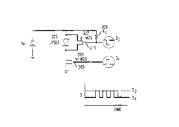
The length of the tail which results in an optical output from a laser diode after the
laser diode is no longer being driven is reduced or eliminated by a laser diode driver with
a tail eliminator. More specifically, the laser diode driver includes an energy drainage
path that is activated when packet communication is over. In one embodiment of
invention, the terminals of the laser diode are short-circuited to provide the energy
drainage path. In another embodiment of the invention, the laser diode is reverse biased,
so that charges stored in the laser diode are combined with charges which are provided
thereto. Advantageously, the tail emission is substantially eliminated.


French Abstract

La durée de la lumière résiduelle émise par une diode laser après l'interruption de l'alimentation de cette dernière est réduite ou annulée à l'aide d'un dispositif d'attaque doté d'un éliminateur de lumière résiduelle. Plus exactement, ce dispositif d'attaque comprend un trajet de drainage d'énergie qui entre en fonction quand la transmission d'un paquet est terminée. Dans l'une des concrétisations de l'invention, les bornes de la diode laser sont court-circuitées pour créer le trajet de drainage d'énergie. Dans une autre concrétisation, la diode laser est polarisée en inverse et les charges qui y sont stockées sont combinées avec d'autres charges qui lui sont fournies. Il en résulte une réduction importante de la lumière résiduelle.

Claims

Note: Claims are shown in the official language in which they were submitted.


What is claimed is:
1. Apparatus for use with a semiconductor laser diode, comprising:
a semiconductor laser diode driving circuit for controllably driving said
semiconductor laser diode; and
means for eliminating excess charges stored in said semiconductor laser diode
when it is not being driven by said semiconductor laser diode driving circuit.
2. The invention as defined in claim 1 wherein said semiconductor laser diode
driving circuit comprises a first MOS transistor and said means for eliminating excess
charges comprises a second MOS transistor.
3. The invention as defined in claim 1 wherein said semiconductor laser diode
driving circuit comprises an MOS transistor of a first type and said means for eliminating
excess charges comprises an MOS transistor of a second type opposite to said first type.
4. The invention as defined in claim 1 wherein said means for eliminating excesscharges stored in said semiconductor laser diode substantially short circuits said
semiconductor laser diode.
5. The invention as defined in claim 1 wherein said means for eliminating excesscharges stored in said semiconductor laser diode reverse biases said semiconductor laser
diode.
6. The invention as defined in claim 1 wherein said means for eliminating excesscharges stored in said semiconductor laser diode reverse biases said semiconductor laser
diode and further includes means for supplying charges to recombine with charges stored
in said semiconductor laser diode.
7. Apparatus for use with a semiconductor laser diode, comprising:
a semiconductor laser diode driving circuit for controllably driving said
semiconductor laser diode; and
means for short circuiting said semiconductor laser diode at least temporarily
when it is not being driven by said semiconductor laser diode driving circuit.
8. Apparatus for use with a semiconductor laser diode, comprising:

a semiconductor laser diode driving circuit for controllably driving said
semiconductor laser diode; and
means for reverse biasing said semiconductor laser diode when it is not being
driven by said semiconductor laser diode driving circuit.
9. The invention as defined in 8 wherein said means for reverse biasing said
semiconductor laser diode includes a capacitor coupled to said semiconductor laser diode,
whereby charges stored in said capacitor combine with charges stored in said
semiconductor laser diode so as to extinguish illumination of said semiconductor laser
diode.
10. The invention as defined in 8 wherein said means for reverse biasing said
semiconductor laser diode includes means for generating a voltage drop.
11. The invention as defined in claim 10 wherein said means for generating a
voltage drop includes a diode.
12. The invention as defined in claim 10 wherein said means for generating a
voltage drop includes a resistor.
13. A method for operating a semiconductor laser diode, comprising the steps of:driving said semiconductor laser diode to supply information encoded as optical
signals; and
reverse biasing said semiconductor laser diode upon conclusion of said driving
step.
14. The invention as defined in claim 13 wherein said information is arranged
into periodic groups, and further wherein said reverse biasing step is performed upon
conclusion of each of said periodic groups.
15. A method for operating a semiconductor laser diode, comprising the steps of:driving said semiconductor laser diode to supply information encoded as optical
signals; and
substantially short circuiting said semiconductor laser diode upon conclusion ofsaid driving step.

16. The invention as defined in claim 15 wherein said information is arranged
into periodic groups, and further wherein said substantially short circuiting step is
performed upon conclusion of each of said periodic groups.

Description

Note: Descriptions are shown in the official language in which they were submitted.


CA 02237~06 1998-0~-13
HIGH SPEED NON-BIASED SEMICONDUCTOR LASER DIODE DRIVER FOR
HIGH SPEED DIGITAL COMMUNICATION
Technicsl Field
This invention relates to optical communication, and more particularly, to a circuit
5 for driving a semiconductor laser diode used in an optical communications link.
Background of the Invention
In prior art high speed passive optical networks (H-PON), no DC optical signal is
allowed in the Up~lle~hll from the optical network unit (ONU) on the customer premises
to the optical line ter~nin~1 (OLT) located in the central office. This requires a
o semiconductor laser diode at the ONU to be operated without bias.
However, when a semiconductor laser diode is operated without bias in the prior
art, the optical output does not turn off immediately after the driving signal is turned off.
That is, a tail is observed in the optical output. Such a situation is illustrated in FIG. 1.
The tail emission is caused by 1) electrical charge that is stored in the laser diode
while it is being driven and 2) the fact that the process of recombination of the charges in
the laser diode is a slow one even after the driving current is removed.
Conventionally, the tail extends over 100 ns. However, in the H-PON, which is a
time shared system in which multiple customer premises ONUs transmit their data in
sequence in their ~lesi~n~te~ time slots, the signal packets from the different customer
20 premises ONUs often wind up being spaced much closer together than the length of the
tail. This implies that a packet from a particular customer premises ONU is influenced by
the tail that was generated by the customer premises ONU which was transmitting a
packet in the time slot imme~ tely precedent to that of the particular customer premises
ONU.
25 Summary of the Invention
I ha~e recognized that it is important to reduce the tail length or to elimin~te the
tail altogether. In accordance with the principles of the invention, this is achieved by a
laser diode driver with a tail e1imin~tor. More specifically, the laser diode driver includes
an energy drainage path that is activated when packet communication is over. In one
30 embodiment of invention, the termin~l~ of the laser diode are short-circuited to provide
the energy drainage path. In another embodiment of the invention, the laser diode is

CA 02237~06 1998-0~-13
reverse biased, so that charges stored in the laser diode are combined with charges which
are provided thereto. Advantageously, the tail emission is subst~nti~lly elimin~te~
Brief Description of the Drawing
In the drawing:
s FIG. 1 shows an example of a tail that results when a semiconductor laser diode is
operated without bias in the prior art, because the optical output does not turn off
immefli~tely after the driving signal is turned off;
FIG. 2 shows a simple prior art arrangement for driving a laser diode without bias;
FIG. 3 shows an exemplary arrangement for driving a laser diode but having an
0 energy drainage path in accordance with the principles of the invention; and
FIG. 4 shows another embodiment of the invention that further acceleldles the
energy drainage process of the laser diode, albeit at the cost of additional conlponents.
Detailed Description
FIG. 2 shows a simple prior art arrangement for driving laser diode (LD) 205
without bias. n-MOS 201 transistor o,oer~les as a switch. When the signal to gate 203 is
high, n-MOS transistor 201 becomes conductive and a current passes through laser diode
205, causing emission of a laser beam. However, when n-MOS transistor 201 is turned
off, by having the signal to gate 203 (S) be low, the stored energy in laser diode 205 has
no path to drain out. Therefore, this stored energy is slowly discharged within the laser
20 diode, and it is this slow discharge that causes the prior art tail.
To alleviate this problem, the circuit shown in FIG. 3 adds an energy drainage
path in accordance with the principles of the invention. Underlying the circuit of FIG. 3
is the circuit of FIG. 2. However, p-MOS transistor 307 and pull-up resistor 309 have
been added to the circuit.
2s In the circuit of FIG. 3, gate 311 of p-MOS transistor 307 is normally set high by
pull-up resistor 303. This results in p-MOS transistor 307 being in the off state. As
before, laser diode 205 is activated when n-MOS transistor 201 is turned on by gate
signal S being high. When the packet communication is over, e.g., in response to a
change in the transmit packet signal already available in the H-PON system, a pulse of
30 "LOW" is applied to gate 311 of p-MOS transistor 307. This pulse makes p-MOS
transistor 3()7 conductive i.e., in the on-state. At the same time, n-MOS transistor 201 is
in the off-state. Therefore, the terminals of laser diode 205 are short-circuited together
and an energy drainage path for the laser diode is formed. Advantageously, the length of
the laser emission tail is shortened.

CA 02237~06 1998-0~-13
FIG. 4 shows another embodiment of the invention that further accelerates the
energy drainage process, albeit at the cost of additional components. More specifically,
diodes 421 and 423, as well as capacitor 425 are added to the circuit shown in FIG. 3.
Diodes 42]. and 423 are high current rectifier diodes. When signal Sl is high, current
passes through diodes 421 and 423, laser diode (LD) 201, and n-MOS transistor 201.
The potential at point A is VO - 2Vth, where Vth is the forward threshold of diodes 421
and 423. Usually, Vth is about 0.7V in a Si rectifier diode. This potential VO - 2Vth is
stored in capacitor 425. When the packet signal Sl is completed, n-MOS transistor 201 is
turned off ~md p-MOS transistor 307 is turned on, by bringing the signal S2 at gate 311
10 thereof low, laser diode 205 is back-biased by 2Vth, and reverse current is supplied from
capacitor 425 and voltage source VO. In this way, laser diode 205 is completely shut-off
and its internal active charges are swiftly elimin~te-l because they recombine with
charges supplied by capacitor 425. Advantageously this circuit subst~nti~lly elimin~tçs
the tail emission.
Note that the use of two diodes is simply an exemplary way of achieving a voltage
drop so that a reverse bias effect results at the laser diode. However, any technique of
achieving a voltage drop may be employed, including,- but not limited to a resistor, a
zener diode, or the like. Those of ordinary skill in the art will recognize that, given the
laser diode o~ldling characteristics and the power supply voltage, the components for
20 achieving the voltage drop should be selected, preferably, to yield the greatest voltage
drop achievable while conc--min~ the least current in the laser diode active state.
As the use of n-MOS and p-MOS transistors are strictly exemplary, those of
ordinary skill in the art will readily recognize how to change the types of transistors
employed. Furthermore, those of o~in~y skill in the art will recognize that it is not
25 nececc~ry to employ opl)osile types of transistors to implement the invention, but instead,
the invention may be implçmentçcl using a single type of transistor.
For pedagogical purposes, note that because of thesholding in reading the signalvalues, the tails that are generated after each one to zero transition by a single ONU are
easily ignored, because the tail power, although a function of the particular laser diode, is
30 typically no more than 10% of the laser diode output power. However, because the laser
diode output power between di~lent ONUs is p~ efl to vary by a very large amount,
e.g., the maximum power may be up to 1000 times greater than the minimum power, the
tail from a laser diode which was generating the m~imnm power will easily dwarf the
signal from the laser diode of the next ONU which is generating only the minimum35 power. In other words, without the invention, tr~ncmicsion errors would develop if the
tail generated by the laser diode of one ONU was too big with respect to the signal

CA 02237.706 1 998 - 0.7 - 1 3
generated by the laser diode of the next ONU. In fact, a small signal could be completely
"buried" by a large tail.
The foregoing merely illustrates the principles of the inventions. It will thus be
appreciated that those skilled in the art will be able to devise various arrangements which,
s although not explicitly described or shown herein, embody the principles of the invention
and are included within its spirit and scope.

Representative Drawing
A single figure which represents the drawing illustrating the invention.
Administrative Status

2024-08-01:As part of the Next Generation Patents (NGP) transition, the Canadian Patents Database (CPD) now contains a more detailed Event History, which replicates the Event Log of our new back-office solution.

Please note that "Inactive:" events refers to events no longer in use in our new back-office solution.

For a clearer understanding of the status of the application/patent presented on this page, the site Disclaimer , as well as the definitions for Patent , Event History , Maintenance Fee  and Payment History  should be consulted.

Event History

Description Date
Inactive: IPC expired 2013-01-01
Inactive: IPC deactivated 2011-07-29
Inactive: First IPC derived 2006-03-12
Inactive: IPC from MCD 2006-03-12
Inactive: Dead - No reply to s.30(2) Rules requisition 2002-08-26
Application Not Reinstated by Deadline 2002-08-26
Deemed Abandoned - Failure to Respond to Maintenance Fee Notice 2002-05-13
Inactive: Abandoned - No reply to s.30(2) Rules requisition 2001-08-27
Inactive: S.30(2) Rules - Examiner requisition 2001-02-26
Application Published (Open to Public Inspection) 1998-12-18
Inactive: IPC assigned 1998-08-11
Classification Modified 1998-08-10
Inactive: First IPC assigned 1998-08-10
Inactive: IPC assigned 1998-08-10
Application Received - Regular National 1998-07-24
Inactive: Filing certificate - RFE (English) 1998-07-24
Request for Examination Requirements Determined Compliant 1998-05-13
All Requirements for Examination Determined Compliant 1998-05-13

Abandonment History

Abandonment Date Reason Reinstatement Date
2002-05-13

Maintenance Fee

The last payment was received on 2001-03-23

Note : If the full payment has not been received on or before the date indicated, a further fee may be required which may be one of the following

  • the reinstatement fee;
  • the late payment fee; or
  • additional fee to reverse deemed expiry.

Patent fees are adjusted on the 1st of January every year. The amounts above are the current amounts if received by December 31 of the current year.
Please refer to the CIPO Patent Fees web page to see all current fee amounts.

Fee History

Fee Type Anniversary Year Due Date Paid Date
Application fee - standard 1998-05-13
Registration of a document 1998-05-13
Request for examination - standard 1998-05-13
MF (application, 2nd anniv.) - standard 02 2000-05-15 2000-03-29
MF (application, 3rd anniv.) - standard 03 2001-05-14 2001-03-23
Owners on Record

Note: Records showing the ownership history in alphabetical order.

Current Owners on Record
LUCENT TECHNOLOGIES INC.
Past Owners on Record
YUSUKE OTA
Past Owners that do not appear in the "Owners on Record" listing will appear in other documentation within the application.
Documents

To view selected files, please enter reCAPTCHA code :


To view images, click a link in the Document Description column (Temporarily unavailable). To download the documents, select one or more checkboxes in the first column and then click the "Download Selected in PDF format (Zip Archive)" or the "Download Selected as Single PDF" button.

List of published and non-published patent-specific documents on the CPD .

If you have any difficulty accessing content, you can call the Client Service Centre at 1-866-997-1936 or send them an e-mail at CIPO Client Service Centre.

({010=All Documents, 020=As Filed, 030=As Open to Public Inspection, 040=At Issuance, 050=Examination, 060=Incoming Correspondence, 070=Miscellaneous, 080=Outgoing Correspondence, 090=Payment})


Document
Description 
Date
(yyyy-mm-dd) 
Number of pages   Size of Image (KB) 
Description 1998-05-12 4 187
Claims 1998-05-12 3 89
Drawings 1998-05-12 2 15
Abstract 1998-05-12 1 17
Representative drawing 1999-01-04 1 3
Courtesy - Certificate of registration (related document(s)) 1998-07-23 1 140
Filing Certificate (English) 1998-07-23 1 174
Reminder of maintenance fee due 2000-01-16 1 113
Courtesy - Abandonment Letter (R30(2)) 2001-11-04 1 171
Courtesy - Abandonment Letter (Maintenance Fee) 2002-06-09 1 183