Note: Descriptions are shown in the official language in which they were submitted.
~ CA 02237679 l998-0j-l4
1 ( a ~D \I~
DO~3LE ~AYER CAPACITOR WITH POROUS CARBON ELECTRODES AND
METHOD FOR MANUFACTURING THESE ELECTRODES.
The present invention relates to a double layer capacitor
comprislng at least two electrodes, substantially o~ porous
carbon, the electrodes being substantially saturated with
electrolyte and separated by means of a porous separator
with ionic conductivity, the electrodes consisting of an
interconnecting solid carbon network.
Such electric devices, more specifically accumulating
constructions for electricity, can be used e.g as a short
time or reserve source o~ electric current ~or a radio
electronic apparatus, for memory units of personal compu-
ters, video and other devices.
The invention also relates to a method of manufacturing an
electrode having a solid carbon skeleton network with a
plur~lity o~ pores and a capacitor electrode material.
One c~ the main directions o~ the development o~ high-
e~iciency capacitors with double electric layer is to make
new electrode carbon materials with such a combination o~
properties as an optimal pore size, mechanical strength and
high chemical purity.
Previously known are capacitors with a double electric
layer (e.g. Japanese patent application No. 3-62296.1991),
comprising two polarized electrodes divided by a separator,
which are placed in a hermetic ~rame. The electrodes are
made of active carbon and a binding agent, which consists
of carbon black and ceramic powder. The electrode material
has a porous structure, resulting in a specific electric
capacitance not more than 25F/cm3.
The deficiencies of such capacitors are:
- considerable leakage currents due to a great content o~
ash in the electrode material (3-8~);
AMENDEO SHEET
CA 02237679 1998-0~-14
2 ~nnR~
- increased variation in capacitance characteristics due to
changeS in microporosity properties o~ the electrode mate-
rial in the process of manufacture of the electrodes and
the capacitor assembly;
- the electrode material has low mechanical strength (this
limits the use of these capacitors in constructions, which
are working under conditlons of high mechanical stress,
e.g. vibrations).
Further, previously known are capacitors with double elec-
tric layer, comprising a ~rame o~ stainless steel; the
frame comprises a bottom and a lid joined by a washer
creating a hermetic container. In the frame, two polarized
electrodes, saturated with electrolyte and separated by a
porous separator, are situated. The electrodes are made of
active carbon (80~ mass) and a binding agent, which con-
sists o~ ash (lO~mass) and polytetrafluorethylene (10~
mass). The material in the ~orm o~ paste is applied to an
e,ectrically conductive underlayer and is then rolled and
dried. From~ the resulting sheet product the prescribed size
electrodes are cut.
Such capacitors can operate over a wide range of tempera-
tures. The electrode material provides speci~ic electric
capacitance within the limits of 20-25 F/cm; However, these
capacitors have all the deficiencies of the preceeding
ones.
An electrode for a double-layer capacitor consisting o~ an
interconnecting solid network is known from EP-A1- 0 660
345.
The object of the present invention is to obtain a simulta-
neous increase in capacitor specific electric capacitance,
decreased variation of the actual capacitance values and
decrease in leakage currents. In addition, the purpose of
the invention is to obtain an increase in electrode
strength and mechanical stability. This will allow an
extension of the field of use for the capacitors, ~or
A~UEND~o SHET
CA 02237679 1998-0~-14
3 (~ ~
example in constructions working under conditions of mecha-
nical impact or vibration To obtain this technical result
a capacitor of the kind mentioned in the beginning of the
description is characterized in that the electrodes have a
pore volume exceeding 55~ of the electrode material volume,
the part of the pores having a size less than 10 nm being
35-S0~ of the electrode material volume The carbon content
of the electrode is more than 95~ mass, preferably more
than 99~ mass The material has a total pore volume pre~e-
rably in the range from 55 to 80~ of the electrode volume;
this makes it possible to obtain a high electric capaci-
tance.
~ The invention also relates to a method of manufacturing an
electrode having a solid carbon skeleton network with a
plurality of pores, characterized by the steps of,
-moulding an electrode blank o~ a metal carbide powder and,
~ as a binding agentl organic binders and carbon, in the form
o~ ca~bon black or as a pyrolysis product, the am.ount 5f
binding agent being 5-50 g per 100 g of metal carbide
powder,
- saturating the moulded blank by liquid metal at a tempe-
rature exceeding the melting temperature but not exceeding
300~ C above this temperature in a vacuum furnace.
- heat treating the saturated blank in halogen gas, such as
fluorine or chlorine, at a temperature of 800 - 1200~ C for
the formation of transport channels/pores and nano porous
(<10 nm) carbon structure. After such a manufacture the
electrode contains practically pure carbon with a ramified
system of transport channels/pores, and only minor amounts
of impurities (less than 5% mass, preferably less than 1~
mass). These electrodes have a carbon structure providing
high electrode mechanical strength (compressive strength
more than 90 kg/cm2). The material consists of a solid
network of carbon interconnected throughout the structure,
resulting in mechanical rigidity and strength, and a com-
A!AENDED SHEET
~ CA 02237679 1998-0~-14
. . .
~ ~ C~
,~' bination of coarser sized transport channels/pores of the
electrolyte and nano sized porosity, together making up the
total porosity volume. Of importance is also the stability
o~ the electrode dimensions and its pores and, as a result,
a stability o~ the electrode electrical properties. Thus,
the decrease in height and diameter values from intermedia-
te product to finished electrode is not more than 0,05~
permitting a very limited variation in electrode speci~ic
electric capacitance, resulting in actual capacitor capaci-
tance in the range +- 15~, whereas known capacitors have
the electric capacitance tolerance + 80 to - 20~.
The new electrodes of~er an increase in speci~ic electric
~ capacitance and actual capacitor capacitance by nearly 30~ -
in comparison with known technical solutions and a decrease
in leakage currents o~ 5-10 times because o~ an only minor
impurity content of the electrode material. In addition,
the high electrode strength makes it possible to use the
~:apacitors in devices working under vibration, impact and
othe~ mechallical stresses.
The invention will now be described in more detail with
reference to exemplifying embodiments thereof and also with
re~erence to the accompanying drawing, in which in ~igure l
an overall capacitor picture is given (side view) and in
-
~ENDED SHEET
CA 02237679 1998-0~-14
WO 97/20333 PCT/EP96tO0431
treatment of a metal carbide composite. After such a
treatment the electrode contains practically pure carbon
with a ramified system of transport channels/pores, and
only minor amounts of impurities (less than 5~ mass,
preferably less than 1% mass). These electrodes have a
carbon structure providing high electrode ?ch~n; cal
strength (compressive strength more than 90 kg/cmZ). The
material consists of a solid network of carbon intercon-
nected throughout the structure, resulting in me~-h~nical
rigidity and strength, and a combination of coarser sized
transport channels/pores of the electrolyte and nano sized
porosity, together making up the total porosity volume. Of
importance is also the stability of the electrode dimen-
sions and its pores and, as a result, a stability of the
electrode electrical properties. Thus, the decrease in
height and diameter values from intermediate product to
finished electrode is not more than 0,05~ permitting a very
limited variation in electrode specific electric capaci-
tance, resulting in actual capacitor capacitance in the
range +- 15%, whereas known capacitors have the electric
capacitance tolerance + 80 to - 20%.
The new electrodes offer an increase in specific electric
capacitance and actual capacitor capacitance by nearly 30%
in comparison with known t~hn; cal solutions and a decrease
in leakage currents of 5-10 times because of an only minor
impurity content of the electrode material. In addition,
the high electrode strength makes it possible to use the
CA 02237679 1998-05-14
WO 97/20333 pcT~r96Joot~
capacitors in devices working under vibration, impact and
other mechanical stresses.
The invention will now be described in more detail with
reference to examplifying embodiments thereof and also with
reference to the acc~ ~-nying drawing, in which in figure l
an overall capacitor picture is given (side view) and in
figure 2 plots of the voltage across the load versus dis-
charge time are given.
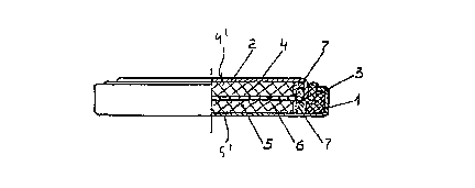
The capacitor with a double electric layer comprises a
hermetic frame, comprising a bottom 1 and a lid 2, joined
by a dielectric washer 3. Inside of the frame electrodes
4, 5 are situated. The electrodes are saturated with an
electrolyte and separated by means of a porous separator 6.
The opposite sides 4', 5' of the double electrode layer are
in contact with the bottom l and lid 2 respectively. To
make assembly of the capacitor more simple there are elas-
tic washers 7 encircling the electrodes peripherally.
For confirmation of the obtained tçchn; cal result 12
pieces of carbon electrodes (diameter 19.5 mm, hight 1.0
mm) and 6 pieces of button like capacitors (diameter 24.5
mm, hight 2.2 mm) were manufactured. As a separator porous
polypropylene with ionic conductivity was used and as
electrolyte an aqueus solution of alkali, KOH, was used.
The nominal electric capacitance of the capacitor was 20F
and the voltage was 1.0 volt.
CA 02237679 1998-0~-14
W O 97/20333 PCTrEP96/00431
The physical and mechanical properties of the electrode
material were investigated and the capacitors were tested
for reliability and possibility to work under actual condi-
tions as a power source for electronic watches and electro-
nic memory units for personal computers. The tests for the
reliability were carried out at the voltage 0.9+-0.1 V. at
a temperature of +70 +-5~ C. The test duration was 500
hours.
The results of the investigation of the electrode physical,
chemical and m~ch~n;cal properties and of the capacitor
tests are given in tables 1 and 2 and by the graphs of
figure 2.
An analysis of the results of electrode investigation
(table 1) shows that the volume of the pores with a size
less than lo nm (average 43% of electrode volume) is nearly
twice that parameter of carbon electrodes manufactured by
means of traditional technology. The compressive strength
increased more than 3 times. The specific electric capaci-
tance (average 34,5 F/cm3) ~c~ by nearly 30% the spe-
cific capacitance of known carbon materials (not more than
25 F/cm3).
The results of the test of reliability (table 2) show only
slight variation of the nominal capacitor capacitance
(+-5,3%). The explanation for this is the high mechanical
strength of the carbon electrodes, having a stable ramified
structure, maint~in;ng geometrical and electrode and elec-
CA 02237679 1998-05-14
WO 97/20333 PCT/EP96/00431
trolyte parameters during the assembly process.
After the test the capacity loss was 5,7~ (average) and the
increase in inner resistance was 18% (average), satisfying
high performance demands.
The results of the test of capacitors show (Fig. 2) that
the duration of the performance of the capacitors as a
current source was: 198 hours at the load 100 kohm, 32
hours at the load 50 kohm, 3 hours at the load 20 kohm and
2 hours at the load 0,5 kohm. These data imitate the real
discharge of capacitors in operation under load in various
devices, where the capacitors may be used as a power
source.
According to a preferred embodiment the electrodes are
produced from silicon carbide powder and, as a binding
agent, a mixture consisting of carbon black, phenolformal-
dehydic resin and ethylated alcohol in the following com-
ponents correlation, mass.%:
Carbon black 30-50
Phenolformaldehydic resin 5-10
Ethylated alcohol 40-60
or pyrocarbon in the amount of 5-50 g per 100 g of silicon
carbide. After moulding, the blank is saturated by li~uid
silicon at the temperature of 1450-1700~ C. Thermo-
chemical treatment by chlorine is conducted at a tempera-
ture of 900-1100~ C.
CA 02237679 1998-0~-14
W O 97/20333 PCT/EP96/00431
The method is described below:
From silicon carbide powder and the binding agent a blank
of given form is moulded. During moulding silicon carbide
powder is mixed with a suspension, the composition, mass.
%, of which is: carbon black 30-50, phenolformaldehydic
resin 5-10, ethylated alcohol 40-60, in the amount of 5-50
g per 100 g of silicon carbide. From this charge the blank
is moulded. Then for curing the resin, heat treatment at a
temperature of 150~ C is conducted. As an alternative a
pyrocarbon binding agent, added to silicon carbide powder
or introduced by heat treatment in a natural gas current,
is used.
Moulded by this method or another moulding t~chn;que the
blank is placed in a vacuum furnace, where saturation by
liquid silicon at a temperature of 1450-1700~ in vacuum is
made. During this process a chemical interaction of liquid
silicon and carbon (carbon black or pyrocarbon) with the
formation of secondary silicon carbide takes place. This
secondary silicon carbide forms throughout all volume of
the blank a continuous structure, bonding the grains of
initial silicon carbide and forming a solid silicon carbon
body with residual pores filled with silicon metal. The
reaction of silicon carbide formation at a temperature
lower than 1450~ C does not occur and the purpose of the
method is not achieved. Silicon begins to evaporate in the
vacuum furnace at temperatures above 1700~ C. Thus, a
porousless blank, comprising silicon carbide particles
CA 02237679 1998-0~-14
WO 97/20333 PCTrEP96/00431
bonded by a structure of secondary silicon carbide and free
silicon, is obtained. Then the blan~ is heat treated by
chlorine at a temperature of 900-1100~ C. During chloration
the free silicon metal is removed from the blank in the
form of gaseous silicon chloride and thus a necessary
volume of transport microporosity channels/pores are
formed. Additionally, as a result o~ silicon car~ide
chloration, carbon with a developed nanoporous structure is
formed.
The combination of transport channels/pores and nano
porosity of the resulting solid carbon network is of great
importance, because it facilitates electrolyte access to
large available internal electrode surfaces, made up by the
nano pore walls. The solid continous carbon network also
provides low internal electrical resistance.
The function of the capacitor according to the invention
should be apparent from the specification given above.
The capacitor according to the invention offers considerab-
le advantages compared to previously known t~chn;ques as
described in the introductory part of the specification.
The invention has been described with reference to an
examplifying embodiment. It will be understood, how-
ever, that other embodiments and minor modifications are
conceivable without departing from the inventive concept.
CA 02237679 l998-0~-l4
W 097/20333 PCT/EP96/00431
For example more than two electrodes may be provided in
the capacitor.
Further, it is possible to produce the electrode material
by means of some other method that provides a structual
network of solid carbon with transport channels/pores and
nano porosity resulting in the mentioned advantages. The
t~ohn;~ues are preparation of a mould comprising metal car-
bide, organic binders and carbon, e.g. in the form of
carbon black or as a pyrolysis product, and metal infiltra-
tion and high-temperature reactions, followed by thermoche-
mical removal of the metal to form the wished solid carbon
structure comprising transport channels/pores and nano
porosity.
An example might be the use of aluminum carbide and alu-
minum metal which lowers the needed reaction temperatures
in the first process step significally. So called cubic
metal carbides based on Ti and other metals of group IV, V
or VI of the periodic system might also be used where
gaseous metal halogenes are formed, like fluorides and
chlorides.
CA 02237679 1998-05-14
PCT/EP96/00431
WO 97/20333
Test results of electrode material Table 1
Elec- Total pores Volume of Specific Compressive Carbon
trodes volume in pores with capaci- st~ength content
electrodessizes less tance
volume than 10 nm
No % % F/cm3kg/cmZ % mass
1 55 45 35 95 99,1
2 70 40 30 99 99,2
3 65 50 39 94 99,3
4 60 45 36 92 99,5
38 93 99,4
6 80 35 31 97 99,2
7 55 50 33 96 99,6
8 75 50 39 100 99,1
9 65 35 30 102 99,3
38 98 99,5
11 60 40 34 97 99,2
12 58 46 35 99 99,4
Test rçsults of manufactured ca~acitors Table 2
Before test 1 After test
Capaci- Actual Resi- Actual Resi- cO-C1X t00 R~-R~ x 100
tors capaci- stance capacl- stance Co R1
tance tance
~o Co,F Ro, Ohm Cl.F Rl. Ohm % %
1 19 0,3 17,8 0,35 6,3 16,6
2 20 0,25 18,6 0,3 7,0 20,0
3 19,5 0,35 18,0 0,4 7,6 14,3
4 18,5 0,25 18,0 0,3 2,8 20,0
18,0 0,3 17,0 0,35 5,6 16,6
6 19.5 0.25 18.5 0.3 5.1 20.0
,
SUBSTITLITE SH~ET (RllLE 26)