Note: Descriptions are shown in the official language in which they were submitted.
CA 02237819 1998-OS-19
1
A MICROMAGNETIC DEVICE FOR POWER PROCESSING
APPLICATIONS AND METHOD OF MANUFACTURE THEREFOR
Technical Field of the Invention
The present invention is directed, in general, to micromagnetic devices and,
more
specifically, to a micromagnetic device for power processing applications, a
method of
manufacture therefor and a power processing circuit employing the same.
Background of the Invention
A magnetic device includes a magnetic core coupled to conductor windings such
that the magnetic flux flows in a closed path about the core. Magnetic devices
are
generally configured in an EE-type arrangement or a toroidal geometry. In the
EE-type
magnetic device, a first and second core-portion of the magnetic core surround
the
conductor windings. In the toroidal magnetic device, a first and second
winding-portion
of the conductor windings surround the magnetic core.
Micromagnetic devices (e.g., microinductors or microtransformers) are micron-
scaled integrated circuit magnetic devices; the electromagnetic properties of
the device
are provided by the presence of the magnetic core and conductor windings. In
the past,
micromagnetic devices were only applicable to low-level signal applications
(e.g.,
recording heads). With the advancement in the production techniques for
integrated
circuits, it is now possible to fabricate micromagnetic devices for relatively
large signal
and power processing applications. For instance, micromagnetic devices may be
employed in power systems for wireless communications equipment.
While many power semiconductor devices (having ferrite cores, for instance)
have
been scaled down into integrated circuits, inductive elements at the present
time remain
discrete and physically large. Of course, there is a strong desire to
miniaturize these
inductive components as well. By extending thin-film processing techniques
employed
in power semiconductor devices to ferromagnetic materials, the size of the
conventional
discrete ferromagnetic-core inductive devices can be reduced significantly.
Ferromagnetic materials such as alloys, however, have much higher saturation
flux
" .",
CA 02237819 2000-04-14
2
densities than ferntes (e.g., 10-20 kG verses 3 kG) thereby reducing the
physical volume of
the core for a given inductance and energy requirement. To limit the eddy
current losses in
the ferromagnetic materials, the materials must be fabricated in inordinately
thin films.
Processing thin-film ferromagnetic materials with traditional rolling and tape
winding
techniques proves to be very costly as the desired tape thicknesses drops
below 0.001 inches
(i. e., 25 ~.m). It is thus advantageous to produce such thin films by other
integrated circuit
deposition techniques such as sputtering or electroplating.
Another germane consideration associated with manufacturing micromagnetic
devices is securing the ferromagnetic material to a silicon substrate or the
like. More
specifically, forming an adequate bond between the ferromagnetic material and
an insulator
coupled to the substrate is an important consideration. Many factors such as
oxide
formation, melting point temperature, interposed contamination, affinity
between materials
and mechanical stress at the interface, influence the adhesion of a thin film
to a substrate.
For instance, one technique readily employed in thin film manufacturing
processes is the
formation of an oxide-metal bond at the interface between the substrate and
the film. The
oxide-metal bond may be formed by employing an oxygen-active metal (such as
tungsten
or chromium) on an oxygen-bearing substrate (such as glass or ceramic) in
conjunction with
a refractory metal (such as tantalum or tungsten). With regard to
contaminants, it is
advantageous to remove any impurities interposed on the substrate. Cleaning
methods vary
in effectiveness and the selected method required depends on the ability of
the deposition
process to dislodge contaminant atoms. As an example, different cleaning
techniques may
be employed with sputtering or electroplating.
Of course, the ultimate consideration with regard to the adhesion properties
depends
on the materials employed. While others have attempted to address the adhesion
of
ferromagnetic materials to an insulator coupled to a substrate [e.g., Measured
Performance
of a High-Power-Density Microfabricated Transformer in a DC-DC Converter, by
Charles
R. Sullivan and Seth R. Sanders, IEEE Power Electronics Specialists
Conference, p. 287-
294 (July 1996)], to date, the problem remains unresolved. Developing an
adhesive material
that simultaneously forms a bond with the insulator and the ferromagnetic
material such
CA 02237819 1998-OS-19
3
that thin-film processing can be applied to inductive elements will provide a
foundation
for the introduction of power micromagnetic integrated circuits.
Accordingly, what is needed in the art is an adhesive for a micromagnetic
device
that can secure a ferromagnetic core to an insulator coupled to a substrate
such that the
micromagnetic device can handle the more stringent requirements associated
with power
processing applications.
Summary of the Invention
To address the above-discussed deficiencies of the prior art, the present
invention
provides, in one aspect, for use with a power micromagnetic device having of a
ferromagnetic core and formed on a substrate having an insulator coupled
thereto, an
adhesive including a metallic material that forms a bond between the insulator
and the
ferromagnetic core to secure the power micromagnetic device to the insulator.
The
present invention also provides a method for securing the ferromagnetic core
of the power
micromagnetic device to the insulator coupled to the substrate employing the
metallic
adhesive.
In related aspects, the present invention provides a power micromagnetic
integrated circuit having a ferromagnetic core, a method of manufacture
therefor and a
power processing circuit employing the same, that includes: ( 1 ) a substrate;
(2) an
insulator coupled to the substrate and (3) a metallic adhesive that forms a
bond between
the insulator and the ferromagnetic core to secure the ferromagnetic core to
the substrate.
The present invention introduces the broad concept of employing a metallic
adhesive to secure a ferromagnetic core to an insulator coupled to a
substrate. As a result,
the limitation associated with depositing a thin-film ferromagnetic material
on an
insulator coupled to a silicon substrate (or the like) is resolved. The bond
formed between
the ferromagnetic material and insulator may be substantially physical,
substantially
chemical or a combination thereof. The present invention, therefore, provides
the
foundation for a micromagnetic device that can handle the requirements
associated with
power processing applications. For the purposes of the present invention, the
metallic
adhesive is an inorganic-based material that is substantially free of
titanium.
CA 02237819 1998-OS-19
4
The foregoing has outlined, rather broadly, features of the present invention
so
that those skilled in the art may better understand the detailed description
of the invention
that follows. Additional features of the invention will be described
hereinafter that form
the subject of the claims of the invention. Those skilled in the art should
appreciate that
they can readily use the disclosed conception and specific embodiment as a
basis for
designing or modifying other structures for carrying out the same purposes of
the present
invention. Those skilled in the art should also realize that such equivalent
constructions
do not depart from the spirit and scope of the invention in its broadest form.
Brief Description of the Drawings
For a more complete understanding of the present invention, reference is now
made to the following descriptions taken in conjunction with the accompanying
drawings,
in which:
FIGURE 1 illustrates a schematic diagram of an embodiment of a power
processing circuit constructed according to the principles of the present
invention;
FIGURE 2 illustrates a top view of an embodiment of a power micromagnetic
device constructed according to the principles of the present invention;
FIGURE 3 illustrates a top view of another embodiment of a power
micromagnetic device constructed according to the principles of the present
invention;
FIGURE 4 illustrates a cross-sectional view of an embodiment of a power
micromagnetic integrated circuit ("PMIC") constructed according to the
principles of the
present invention; and
FIGURE 5 illustrates a flow diagram of an embodiment of a method of
manufacturing the power micromagnetic integrated circuit ("PMIC") of FIGURE 4.
Detailed Description
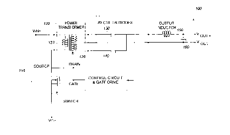
Referring initially to FIGURE 1, illustrated is a schematic diagram of an
embodiment of a power processing circuit 100 constructed according to the
principles of
the present invention. The power processing circuit 100 includes a power train
having a
conversion stage including a switching circuit 110 for receiving input
electrical power V~
CA 02237819 1998-OS-19
and producing therefrom switched electrical power. The power processing
circuit 100
further includes a filter circuit (including an output inductor 150 and output
capacitor 160)
for filtering the switched electrical power to produce output electrical power
(represented
as a voltage Vou.l.). The power processing circuit 100 still further includes
a power
5 micromagnetic integrated circuit (e.g., transformer) 120, having a primary
winding 123
and a secondary winding 126, and a rectifier (including rectifying diodes 130,
140)
coupled between the power conversion stage and the filter stage. The
transformer 120 is
constructed according to the principles of the present invention as
hereinafter described.
The transformer 120 and power processing circuit 100 are submitted for
illustrative
purposes only and other power micromagnetic integrated circuits and
applications therefor
are well within the broad scope of the present invention.
Turning now to FIGURE 2, illustrated is a top view of an embodiment of a power
micromagnetic device 200 constructed according to the principles of the
present
invention. The power micromagnetic device 200 is an EE-type transformer
device. The
power micromagnetic device 200 includes a ferromagnetic core having a first
core-portion
210 and a second core-portion 220. While the ferromagnetic core may be
composed of
an alloy [e.g., a permalloyTM composed of nickel-iron including about 80%
nickel and
20% iron), other ferromagnetic materials are well within the broad scope of
the present
invention. The power micromagnetic device 200 also includes conductive
windings
having a primary winding 230 and a secondary winding 240. Of course, the
windings
may be formed from any conductive material. The primary winding 230 terminates
in a
plurality of terminals 250, 260; the secondary winding 240 terminates in a
plurality of
terminals 270, 280.
The first and second core-portions 210, 220 surround the primary and secondary
windings 230, 240. The magnetic flux of the power micromagnetic device 200
predominantly flows along the width of the ferromagnetic core. As a result,
the
ferromagnetic . core is anisotropic thereby controlling hysteresis losses at
higher
frequencies (e.g., above 10 MHZ). The anisotropic property may be introduced
by a
deposition process in a uniform magnetic field through an energized solenoid
or
permanent magnet at levels of 10-500 Oersteds [("Oe"); 8000 - 40000 A/m]. The
induced
CA 02237819 1998-OS-19
6
anisotropy also produces a hard and easy axis, along which the permeability is
a minimum
and maximum. In some cases, the permeability is increased five-fold from the
hard axis
to the easy axis as a result of the anistropy. The EE-type structure
effectively controls the
permeability of the ferromagnetic core by regulating the direction of the
induced
anisotropy with respect to the magnetic field vector. The first and second
core-portion
230, 240 are coupled together by magnetic vias (when anisotropic
characteristics and
control are desired) or remain separate (when an air gap is desired).
With regard to the ferromagnetic material, the total thickness thereof is
selected
based on the inductance requirements of the device. For operation at
relatively high
frequencies (e.g., above 10 MHZ), eddy currents induced in the ferromagnetic
materials
can become problematic due to the resulting low resistivity (e.g., p ~ 20-100
p'Llcm). To
reduce the eddy currents, the magnetic film thickness of the ferromagnetic
material should
be limited to a fraction of the skin depth 8 [where 8 = (p/nf~.)~' for a given
frequency f
of operation]. For instance, at 8 MHZ and ~=1000, the skin depth is about 2.5
~.m; thus,
to limit the effect of the eddy currents the film thickness should be below
about 2pm
(obviously, thinner films are necessary as the permeability increases). When
the
inductance specification requires a larger thickness, insulated multiple
layers of film (with
each layer not exceeding the necessary skin thickness) should be employed.
Turning now to FIGURE 3, illustrated is a top view of another embodiment of a
power micromagnetic device 300 constructed according to the principles of the
present
invention. The power micromagnetic device 300 is a toroidal transformer
device. The
power micromagnetic device 300 includes a ferromagnetic core 310 (proximate a
window
325) and conductive windings (collectively designated 350) that surround the
ferromagnetic core 310 through inner-layer connection vial (one of which as
designated
375) and terminate in a plurality of terminals 380, 385, 390, 395. The inner-
layer
connection vias 375 lie within the window 310. The line space rules and
distance
between via requirements determine the size of the window 310. Obviously, with
the
trend moving toward smaller devices, a smaller window dimension is desirable.
The
dimension of the window 310, however, is limited as dictated by the thickness
of the
ferromagnetic material necessary to achieve the inductance characteristics.
The
CA 02237819 1998-OS-19
inductance, as an example, for a toroidal device is maximized if the toroid is
generally
circular; the inductance is less if the toroid is formed into a square (~25%
less) and finally
degrades as the square is elongated into a rectangle. The inductance for a
square toroid
having a core width to meet a minimum window dimension, is:
L=~°[NZt]/4(1 + n)
where N is the number of turns of the winding and t is the thickness of the
film. The size
of the window 310 is determined by the minimum via size, via-via clearance and
the
number of vias (related to the number of primary and secondary turns).
Therefore, to
reduce the die size of the device, a larger core thicknesses is necessary to
obtain an
equivalent inductance to an EE ferromagnetic core of equal winding turns and
core width.
Remember that for the EE-type structure fewer winding connection vias are
required thereby reducing the amount of die space necessary to couple the
windings to the
core. Toroidal transformers, however, offer a relatively flat and smooth
surface for the
deposition of the ferromagnetic material thereby reducing the formation of
stresses that
may cause the degradation of the magnetic properties of the film deposited
thereon. This
is especially important when the ferromagnetic material has a high
magnetostriction
constant. The EE-type structure, also, requires special provisions to create a
continuous
magnetic path from the first core-portion to the second core-portion. This is
accomplished by introducing vial within the central core region and at the two
outer core
edges. The vial provide connectivity for the ferromagnetic material such that
the first and
second core-portions are coupled together continuously. The vial, however, are
a source
of stress concentration that require additional slope reduction to decrease
the accumulated
stresses.
While the preceding FIGURES illustrate both the EE-type and toroidal
transformer
device (including the advantages and disadvantages therefor), other power
micromagnetic
devices (including variations of the foregoing devices) and applications
therefor are well
within the broad scope of the present invention.
Turning now to FIGURE 4, illustrated is a cross-sectional view of an
embodiment
of a power micromagnetic integrated circuit ("PMIC") 400 constructed according
to the
principles of the present invention. The PMIC 400 includes a substrate
(composed of, for
CA 02237819 1998-OS-19
8
instance, silicon, glass, ceramic or the like) 410 having a passivation layer
(e.g., silicon-
dioxide) 420 formed thereon using conventional formation processes such as a
thermal
growing process. The PMIC 400 further includes a first and second conductive
winding
layer (composed of, for instance, aluminum or any other conductive material)
440, 460
surrounded by first, second and third insulative layers or insulators 430,
450, 470. The
PMIC 400 still further includes a metallic adhesive that contains a first
adhesive layer
(e.g., chromium) 480 and a second adhesive layer (e.g., silver) 485. The PMIC
400 still
further includes a ferromagnetic core 490. The PMIC 400 still further includes
a plurality
of inner-layer vias (collectively designated 493) that provide multiple paths
between
layers of the PMIC 400 and a terminal 496 for connection to another device.
The
passivation layer 420 and first, second and third insulative layers 430, 450,
470 may be
formed from an inorganic composition (e.g., silicon-dioxide, aluminum-dioxide,
beryllium-dioxide), an organic polymer (e.g., a polyimide) or any other
insulating
material. As previously mentioned, the metallic adhesive is an inorganic-based
material
that is substantially (about 70%) free of titanium. While the first adhesive
layer 480
generally contains materials selected from Group 4 elements (such as zirconium
and
hafnium; excluding about a 70% or more composition of titanium), Group S
elements
(such as vanadium, niobium and tantalum) and Group 6 elements (such as
chromium,
molybdenum and tungsten), other elements are well within the broad scope of
the present
invention. It should be noted that the above classifications of elements are
compatible
with the new International Union of Pure and Applied Chemistry notation
indicated in the
periodic table. Additionally, while the second adhesive 485 generally contains
metals
such as gold, silver, platinum, palladium and copper, other materials
susceptible to plating
a ferromagnetic material are well within the broad scope of the present
invention. Again,
while the ferromagnetic core 490 may be composed of an alloy [such as the
permalloyTM
or a cobalt-iron composition), other ferromagnetic materials (e.g., an
amorphous nickel
phosphide) are well within the broad scope of the present invention.
As previously mentioned, it is desirable to manufacture micromagnetic devices
as integrated circuits. Employing alloys in the ferromagnetic core 490 is
attractive
because of the relatively low magnetostriction constants thereby reducing the
stress
CA 02237819 1998-OS-19
9
associated with the deposition processes. If relatively high stresses are
associated with
the deposition process, the magnetic properties of the PMIC 40 may be degraded
and the
thin films may lack the requisite adhesive properties necessary to facilitate
the deposition
of the PMIC 400. Obviously, a metallic adhesive should be provided that
counteracts the
potential built-up stress in the films.
Several attempts have been undertaken to uncover a metallic adhesive that
provides a secure interface to a ferromagnetic material and an insulator. For
instance,
when a metal such as sliver is exclusively used as the metallic adhesive, the
ferromagnetic
material/silver interface is stronger than the insulator/silver interface. As
a result, the
ferromagnetic material and silver films may be peeled away from the substrate
at a
specified testing peel force (using a standard adhesion evaluation technique
for less than
1 kG/cm2). Conversely, when chromium is exclusively used as the metallic
adhesive, the
insulator/chromium interface is stronger than the ferromagnetic
material/chromium
interface. As a result, the ferromagnetic material and silver films may be
peeled away
from the substrate at a specified testing peel force (using a standard
adhesion evaluation
technique for less than 1 kG/cm2). Additionally, the chromium does not provide
an
adequate seed layer for plating the ferromagnetic material. The present
invention,
therefore, introduces a metallic adhesive that provides an adequate bond
between the
ferromagnetic core 490 and the insulators 430, 450, 470 coupled to the
substrate 410 to
facilitate the fabrication of the PMIC 400.
Turning now to FIGURE 5, illustrated is a flow diagram of an embodiment of a
method of manufacturing the PMIC of FIGURE 4. The method of manufacturing the
PMIC is analogous to conventional silicon-on-silicon multi-chip-module
processes [see
Silicon-on-Silicon MCMs with Integrated Passive Components, by R.C. Frye, et
al., Proc.
1992 IEEE Multi-Chip Module Conference, 155, Santa Cruz, Ca. (1992), which is
herein
incorporated by reference) with the following variations. Generally, a
photolithographic
process with photoresist is used to define the geometrical features of the
PMIC based
upon a 20 ~m design rule. While the rule is relatively coarse, it is adequate
for
fabricating devices such as the PMIC since the major dimensions are multiples
of the 20
~m rule. The photolithographic process generally includes the steps of
exposing and
CA 02237819 1998-OS-19
developing the photoresist and etching away and stripping the unwanted
portions of the
material that the process is being applied to away from the circuit. Those
skilled in the
art should be familiar with conventional photolithographic processes.
'The PMIC employs a toroidal structure that includes multiple layers. The
method
5 begins at a start step 510. A silicon substrate is oxidized with a
passivation layer an
oxidize substrate step 520. The passivation layer is generally created using
conventional
thermal growing techniques or chemical vapor deposition techniques. Of course,
the
substrate may be blank or be composed of a pre-fabricated wafer with
underlying circuitry
and final passivation. The first conductive winding layer is, then, blanket
deposited on
10 the substrate during a deposit first conductive winding layer 530. The
first conductive
winding layer may be composed of aluminum that is sputter deposited (for
instance, at
5 mtorr Argon pressure and room temperature) on the passivation layer having a
thicknesses of about 2-10 p.m. For thicker conductor traces (to achieve lower
resistance),
electroplated copper may be used to obtain thicknesses up to about 25 Vim. The
first
conductive winding layer is then patterned to the desired configuration
(including the
desired contact regions for the PMIC) using a conventional photolithographic
process.
Of course, another contact region may be formed in the first conductive
winding layer to
facilitate electrical connectivity to other circuits coupled to the substrate.
The first
insulative layer is spin coated on the passivation layer and the first
conductive winding
layer during a deposit first insulative layer step 540. The first insulative
layer is cured (at
about 350°C for approximately l2~hours) and after shrinkage an
insulative layer of about
3-5 ~m thick is produced. The spin coating techniques, generally, provide
higher voltage
isolation between the primary and secondary windings; generally, the voltage
level
breakdown values for isolation vary from 500 volts alternating current ("VAC")
to 1500
VAC. The first insulative layer is then patterned using a photolithographic
process to
form the inner-layer vias therethrough.
The metallic adhesive including the first and second adhesive layers are
blanket
deposited on the first insulative layer during an apply metallic adhesive
layer step 550.
The first adhesive layer may be composed of chromium that is sputter deposited
(for
instance, at 5 mtorr Argon pressure and 250°C) on the first insulative
layer having a
CA 02237819 1998-OS-19
11
thicknesses of about 250 A°. The second adhesive layer may be composed
of silver that
is sputter deposited (for instance, at 5 mtorr Argon pressure and room
temperature) on the
first adhesive layer having a thicknesses of about 500 A°. The metallic
adhesive also
serves as a seed layer for plating the ferromagnetic core. The ferromagnetic
core is
deposited (e.g., electroplated in a thicknesses of about 2-12 Vim) on the
metallic adhesive
during a deposit ferromagnetic core step 560. The ferromagnetic core may be
plated in
a buffered sulfamate bath under a controlled temperature (e.g., 25-
35°C) with a current
density of about 30 mA/cm2. The metallic adhesive and ferromagnetic core are
patterned
to the desired configuration using a photolithographic process. With regard to
the
photolithographic process, the etching solutions should be capable of removing
the
unwanted metallic adhesive (e.g., chromium-silver composition) without
attacking the
deposited ferromagnetic film. For instance, a standard commercial cerric
ammonium
nitrate ("CAN") formulation etch solution etches the silver at the rate of
about 50 A°/sec
and the chromium at the rate of 250 A°/min without substantially
affecting the
1 S ferromagnetic material. Thus, employing a CAN etch for approximately 60-75
seconds
is adequate to pattern the metallic adhesive and ferromagnetic core. Again,
the first
adhesive layer (e.g., chromium) is preferably deposited in the range of 200-
300 (250
nominal) A° and the second adhesive layer (e.g., silver) is preferably
deposited in the
range of 400-600 (500 nominal) A° to facilitate a controllable etch
process.
Furthermore, to eliminate possible lateral etching and undercutting beneath
the
ferromagnetic core, the second adhesive layer may be composed of copper. In
this case,
a potassium iodide and water solution may be applied for about 10 seconds to
perform the
copper etching process and a potassium ferri-cyanide and potassium hydroxide
solution
may be applied for about 1-2 seconds to perform the chromium etching process.
The
potassium ferri-cyanide and potassium hydroxide solution does not
substantially affect
the copper layer underlying the ferromagnetic core thereby preventing the
potential affects
of undercutting. Of course, other types of etching processes (such as ion
etching) are
well within the broad scope of the present invention.
The second insulative layer is spin coated on the ferromagnetic core and the
first
insulative layer during a deposit second insulative layer step 570. The second
insulative
CA 02237819 1998-OS-19
12
layer is then patterned using a photolithographic process to form the inner-
layer vias
therethrough. The second conductive winding layer is, then, blanket deposited
(e.g.,
sputtered) on the second insulative layer during a deposit the second winding
conductive
layer step 580. The second conductive winding layer is then patterned to the
desired
configuration (including the desired contact regions) using a
photolithographic process.
Next, the third insulative layer is spin coated on the second conductive
winding layer and
the second insulative layer during a deposit third insulative layer step 590.
A terminal is
finally formed in the third insulative layer during a form terminal step 599.
The terminal
is suitable for wire bonding (e.g., aluminum wire bonding) or is finished with
a solder-
wettable metal (e.g., chromium) for use with solder pastes for flip-chip
assembly. The
method terminates at an end step 599. A completed wafer may then be packaged
as an
integrated circuit or bare die mounted as in flip-chip assemblies.
While FIGURES 4 and 5 illustrate an embodiment of a power micromagnetic
integrated circuit and method of manufacture (including the photolithographic
process)
therefor, other power micromagnetic integrated circuits (including variations
of the
foregoing circuit) and methods of manufacture therefor are well within the
broad scope
of the present invention.
For a better understanding of power electronics, power magnetic devices and
power converter topologies see Principles of Power Electronics, by J.
Kassakian, M.
Schlecht, Addison-Wesley Publishing Company (1991). For a better understanding
of
integrated circuits and methods of manufacture therefor see Handbook of
Sputter
Deposition Technology, by K. Wasa and S. Hayakawa, Noyes Publications (1992)
and
Thin Film Technology, by R.W. Berry, P.M. Hall and M.T. Harns, Van Nostrand
(1968);
Thin Film Processes, by J. Vossen and W. Kern, Academic ( 1978); and Handbook
of Thin
Film Technology, by L. Maissel and R. Glang, McCrraw Hill (1970). The
aforementioned
references are herein incorporated by reference.
Although the present invention has been described in detail, those skilled in
the
art should understand that they can make various changes, substitutions and
alterations
herein without departing from the spirit and scope of the invention in its
broadest form.