Note: Descriptions are shown in the official language in which they were submitted.
CA 02237984 1998-OS-19
TIME-DIVISION MULTIPLEXING TRANSMISSION SYSTEM
BACKGROUND OF THE INVENTION
Field of the Invention
The present invention relates to a time-division
multiplexing transmission system, and more
particularly to a time-division multiplexing
transmission system for performing channel
identification in the case where each of a plurality
of signals including at least one frame structure
signal having frame structure is multiplexed as one
channel and transmitted in a time-division manner.
Description of the Prior Art
A conventional time-division multiplexing
transmission system is disclosed in Japanese Patent
Application Laid-Open No. 2-253735. A description will
be made of this conventional system in reference to
Fig. 15.
In the figure, in the conventional system, a
frame synchronization signal is first added to a
specific channel signal by a frame synchronization
signal addition circuit 111. Then, signal addition
circuits 112 to 114 add signals differing from the
frame synchronization signal to the other channels
instead of adding respective frame synchronization
CA 02237984 1998-OS-19
-2-
signals. Next, these channel signals are multiplexed
and transmitted on a transmission path by a
multiplexer 121.
A demultiplexer 131 demultiplexes the output
signal from the multiplexer into four indivisual
channel signals. Frame synchronization is performed on
the four channels by frame synchronization signal
detection circuits 141 to 1.44. At this time, it can be
judged that the channel in which frame synchronization
has been established is the above-mentioned specific
channel. A channel switching circuit 151 performs a
switch of the channels on the basis of the outputs of
the frame synchronization signal addition circuits 141
to 144.
In the above-mentioned conventional time-
division multiplexing transmission system, at the
transmitter side there is a need to add a new frame
synchronization signal to a specific channel and add
signals differing from the frame synchronization
signal to the other channels. For this reason, the
channels require signal addition circuits respectively,
and consequently, there is a disadvantage that the
entire size of the system is increased.
Also, this conventional transmission system has
another disadvantage that it requires circuitry which
operates at a higher transmission rate, because the
above-mentioned signals are added.
CA 02237984 2002-O1-25
75120-11
-3-
BRIEF SUMMARY OF THE INVENTION
The present invention has been made in order to
solve the above-mentioned disadvantages of the prior art,
and the objective is to provide to a time-division
multiplexing transmission system which is structurally
simple and where there is no increase in the size.
In accordance with the present invention, there is
provided a time-division multiplexing transmission system
for multiplexing and transmitting a plurality of channels of
signals which include at least one frame structure signal
having frame structure in a time-division manner, the time-
division multiplexing transmission system comprising: a
transmitter having inversion means for inverting at least
some of synchronization patterns in said frame structure
signal, and time-division multiplexing means for
multiplexing and transmitting a plurality of channels of
signals which include said frame structure signal having the
inverted synchronization patterns in a time-division manner;
and a receiver having demultiplexing means for
demultiplexing the time-division multiplexed channels into
individual channels, frame synchronization means for
performing frame synchronization on the demultiplexed
channel having the inverted synchronization patterns by
detecting the inverted synchronization patterns, and channel
identification means for using the frame synchronized
channel as a reference and recognizing the remaining
channels.
In accordance with the present invention, there is
also provided a transmitter which is employed in a time-
division multiplexing transmission system for multiplexing
and transmitting a plurality of channels of signals which
include at least one frame structure signal having frame
CA 02237984 2002-O1-25
75120-11
-4-
structure in a time-division manner, the transmitter
comprising: inversion means for inverting at least some of
synchronization patterns in said frame structure signal; and
time-division multiplexing means for multiplexing and
transmitting a plurality of channels of signal which include
said frame structure signal having the inverted
synchronization patterns in a time-division manner.
In accordance with the present invention, there is
further provided a receiver which is employed in a time-
division multiplexing transmission system for multiplexing
and transmitting a plurality of channels of signals which
include at least one frame structure signal having frame
structure in a time-division manner, the receiver comprising
demultiplexing means for demultiplexing the time-division
multiplexed channels into individual channels; frame
synchronization means for performing frame synchronization
on the demultiplexed channel having the inverted
synchronization patterns by detecting the inverted
synchronization patterns; and channel identification means
for using the frame synchronized channel as a reference and
recognizing the remaining channels.
In the transmitter, at least some of
synchronization patterns in a signal having frame structure
are inverted, and a plurality of channels of signals which
include a signal having the inverted synchronization
patterns are multiplexed and transmitted in a time-division
manner. In the receiver, the time-division multiplexed
channels are demultiplexed into individual channels. Then,
frame synchronization is performed on the basis of the
channel having the inverted synchronization patterns among
the demultiplexed channels. With the frame synchronized
channel as a reference, the remaining channels are
identified. With this constitution, the system becomes
CA 02237984 2002-O1-25
75120-11
-4a-
structurally simple and there is no possibility that the
size of the system will be increased.
BRIEF DESCRIPTION OF THE DRAWINGS
The present invention will be described in further
detail with reference to the accompanying drawings in which:
Fig. 1 is a block diagram showing the constitution
of a time-division multiplexing transmission system
according to an embodiment of the
CA 02237984 1998-OS-19
-5-
present invention;
FIG. 2 is a timing chart showing the operation
of the time-division multiplexing transmission system
in FIG. 1;
FIG. 3 is a block diagram showing the interior
constitution of the time-division multiplexing
transmission system in FIG. 1;
FIG. 4 is a block diagram showing the interior
constitution of the demultiplexer in FIG. 1;
FIG. 5 is a timing chart showing the operation
of the demultiplexer in FIG. 4;
FIG. 6 is a circuit diagram showing the
constitution of a division circuit with a phase shift
function for producing a 1/4 clock signal in the
demultiplexer of FIG. 4;
FIG. 7 is a timing chart showing the operation
of the division circuit with a phase shift function of
FIG. 6;
FIG. 8A and FIG. 8B are diagrams showing the
frame format of an SDH signal;
FIG. 9 is a block diagram showing another
embodiment of the receiver in the time-division
multiplexing transmission system of the present
invention;
FIG. 10 is a block diagram showing the interior
constitution of the channel switching circuit in FIG.
9:
CA 02237984 1998-OS-19
-6-
FIG. 11 is a block diagram showing another
embodiment of the transmitter in the time-division
multiplexing transmission system of the present
invention;
FIG. 12 is a block diagram showing still another
embodiment of the receiver in the time-division
multiplexing transmission system of the present
invention;
FIG. 13 is a block diagram showing an
constitution example of the frame synchronization
channel identification circuit of the present
invention;
FIG. 14 is a block diagram showing the interior
constitution of the frame synchronization circuit in
FIG. 13; and
FIG. 15 is a block diagram showing the
constitution of a conventional time-division
multiplexing transmission system.
DETAILED DESCRIPTION OF THE PREFERRED EMBODIMENTS
A preferred embodiment of the present invention
will hereinafter be described in reference to the
drawings.
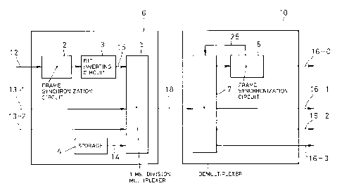
FIG. 1 shows an embodiment of a time-division
multiplexing transmission system employing a channel
identification method according to the present
invention. As shown in the figure, the system
CA 02237984 1998-OS-19
_7_
according to the present invention is constituted by a
transmitter 6 which receives a signal 12 and outputs a
signal 18 after time-division multiplexing and a
receiver 10 which receives the signal 18 from the
transmitter 6 and outputs channels to the output ports
16-0 to 16-3.
The transmitter 6 is constituted by a frame
synchronization circuit 2 which performs frame
synchronization by detecting a synchronization pattern
from the signal 12 having frame structure, a bit
inverting circuit 3 which inverts some or all of the
synchronization pattern in the signal on the basis of
a flag indicating the temporal position of a frame
synchronization byte, a storage 4 which outputs a
free-format signal 14, and a time-division multiplexer
5 which multiplexes channel 0 (reference signal) of
the bit-inverted signal 15 and other channels in a
time-division manner.
The receiver 10 is constituted by a
demultiplexer 7 which demultiplexes the time-division
multiplexed signal 18 into indivisual channels and a
frame synchronization circuit 8 which performs frame
synchronization on the signal 15 within the
transmitter 6 by monitoring all the indivisual
channels and then detecting the bit inverted
synchronization pattern.
In such constitution, the signal 12 with frame
CA 02237984 1998-OS-19
_g_
structure, fetched from a network, is input to the
frame synchronization circuit 2 of the transmitter 6.
This frame synchronization circuit 2 performs frame
synchronization by detecting the synchronization
pattern.
The frame synchronization circuit 2 outputs the
signal 12 having frame structure and also outputs a
flag indicating the temporal position of a
synchronization byte in the signal. The bit inverting
circuit 3 inverts some or all of synchronization
patterns in the signal, based on the flag indicating
the temporal position of a synchronization byte. In
this case the position at which a bit is inverted has
previously been determined.
That is, as shown in FIG. 2, the flag and frame
synchronization byte b which are output from the frame
synchronization circuit 2 are output at intervals of a
constant time d. The bit inverting circuit 3 inverts a
byte after time d from the rising edge of the flag. A
specific description as to which byte is inverted will
be described later.
The output signal 15 of the bit inverting
circuit 3 which has bit-.inverted frame structure is
used as channel 0 (reference channel), and channel 0
and other channels are multiplexed in a time-division
manner by the time-division multiplexer 5. After this
time-division multiplexing, the output signal 18 is
CA 02237984 1998-OS-19
-9-
transmitted from the transmitter 6 to the receiver 10.
In this embodiment, the contents of channel 1
and channel 2 are signals 13-1 and 13-2 with frame
structure, fetched from a network. The content of
channel 3 is a free-format signal 14 which is output
from the storage 4. The free format means that signal
format does not matter with respect to a certain
signal.
Assume that the content of each channel other
than channel 0 may be a signal with frame structure as
in the signals 13-1 and 13-2 or may be a signal with
entirely original format like a free-format signal 14.
The frame structure of the signal 12 and the frame
structures of the signals 13-1 and 13-2 may be the
same kind or different kinds.
The same kind of frame means a frame having the
same frame synchronization byte and having the same
frame length. Therefore, a frame synchronization
circuit is common to frames of the same kind, and
frames of the same kind cannot be discriminated from
each other by frame synchronization alone.
On the other hand, a different kind of frame
means a frame having a different frame synchronization
byte or a different frame length. Therefore, frames of
different kinds can be discriminated each other if
only frame synchronization is performed.
As shown in FIG. 3, the time-division
CA 02237984 1998-OS-19
- 10-
multiplexes 5 within the transmitter 6 comprises D
flip-flops 51-1 to 51-4 (hereinafter referred to as D-
F/Fs) provided in correspondence to each signal
constituting the parallel signals and to which
parallel signals are input, a D-F/F 52-1 to which the
output signal of the D-F/F 51-1 is input, a load
change-over switch 53-1 which selectively outputs the
output signal of the D-F/F 52-1 and the output signal
of the D-F/F 51-2, and a D-F/F 52-2 to which the
output signal of the switch 53-1 is input. A 1/4 clock
signal 700 is input to each of the D-F/Fs 51-1 to 51-4.
As shown in the figure, the time-division
multiplexes 5 is constituted by a load change-over
switch 53-2 which selectively outputs the output
signal of the D-F/F 52-2 and the output signal of the
D-F/F 51-3, and a D-F/F 52-3 to which the output
signal of the switch 53-2 is input, a load change-over
switch 53-3 which selectively outputs the output
signal of the D-F/F 52-3 and the output signal of the
D-F/F 51-4, and a D-F/F 52-4 to which the output
signal of the switch 53-3 is input. A load change-over
signal (load switching signal) 50 is input to the load
change-over switches 53-1 to 53-3, and a clock signal
70 is input to the D-F/Fs 52-1 to 52-4.
In such constitution, parallel signals are input
to the D-F/Fs 51-1 to 51-4 when a rising edge occurs
on the 1/4 clock signal 700. The output signals of the
CA 02237984 1998-OS-19
D-F/Fs 51-1 to 51-4 are input to the D-F/Fs 52-1 to
52-4 when a rising edge occurs on the clock signal 70.
At this time, if the level of the load change-over
signal 50 changes, the output levels of the load
change-over switches 53-1 to 53-3 will change. For
this reason, the signal 18 which is finally output
becomes a signal in which four channels are
multiplexed in a time-division manner.
Next, the receiver 10 receives the output signal
18 of the transmitter 6. The demultiplexer 7
demultiplexes the output signal 18 into indivisual
channels. The frame synchronization circuit 8 monitors
all the indivisual channels and detects a bit-inverted
synchronization pattern, whereby frame synchronization
is performed on the signal 15 having bit-inverted
frame structure.
A method of monitoring all channels is as
follows: Channels are monitored in order in a time-
division manner with a single frame synchronization
circuit. In this case the demultiplexer 7 is provided
with a bit rotating function. When a serial signal is
demultiplexed into parallel signals, the bit rotating
function changes the phases of the parallel signals,
thereby rotating the ports from which the parallel
signals are output. In this embodiment, when frame
synchronization is not obtained for a fixed time by
the frame synchronization circuit 8, bit rotation is
CA 02237984 1998-OS-19
-12-
performed once at a time.
Now, a description will be made of the interior
constitution example of the demultiplexer 7 having a
bit rotating function in reference to FIG. 4. As shown
in the figure, the demultiplexer 7 is constituted by
four serial D-F/Fs 71-1 to 71-4 which operate in
synchronization with the clock signal 70 and four D-
F/Fs 72-1 to 72-4 to which the output signals of the
D-F/Fs 71-1 to 71-4 are input and which operate in
synchronization with the 1/4 clock signal 700 which
divides the clock signal 70 by 1/4.
The operation of the demultiplexer 7 having such
constitution will be described in reference to FIG. 5.
In addition to the output states of the D-F/Fs 71-1 to
71-4 of FIG. 4, FIG. 5 shows the 1/4 clock signal 700,
the output states (1) of the D-F/Fs 71-1 to 71-4
before bit rotation, and the output states (2) of the
D-F/Fs 71 to 71-4 after bit rotation.
In FIG. 5, four channels of data have been input
to the D-F/Fs 71-1 to 71-4. The four channels of data
are 11, 12, 13, 14, 15 ..., 21, 22, 23, 24, 25 ..., 31,
32, 33, 34, 35 ..., and 41, 42, 43, 44, 45 .... Since
these channels of data are input to the receiver 10
after they have been multiplexed in a time-division
manner, the D-F/Fs 71-1 to 71-4 output 11, 21, 31, 41,
12, 22, 32, 42, 13, 23, 33, 43, 14, 24, 34, 44, 15, 25,
35, 45 ... in the recited arder.
CA 02237984 1998-OS-19
-13-
In the state (1) before bit rotation, the output
signals of the D-F/Fs 71-1 to 71-4 are input in
sequence to the D-F/Fs 72-1 to 72-4 when a rising edge
occurs on the 1/4 clock signal 700. For this reason,
the D-F/F 72-1 outputs 41, 42, 43, 44 .... The D-F/F
72-2 outputs 31, 32, 33, 34 .... The D-F/F 72-3
outputs 21, 22, 23, 24 .... The D-F/F 72-4 outputs 11,
12, 13, 14 ....
On the other hand, the case where bit rotation
is performed by two bits by changing the phase of the
1/4 clock signal 700 is the state (2) after bit
rotation. Even in the state (2), the output signals of
the D-F/Fs 71-1 to 71-4 are input in sequence to the
D-F/Fs 72-1 to 72-4 when a rising edge occurs on the
1/4 clock signal 700. For this reason, the D-F/F 72-1
outputs 21, 22, 23, 24 .... The D-F/F 72-2 outputs 11,
12, 13, 14 .... The D-F/F 72-3 outputs 41, 42, 43,
44 .... The D-F/F 72-4 outputs 31, 32, 33, 34 ....
Thus, if the phase of the 1/4 clock signal 700
is changed, the ports which are output as parallel
signals can be rotated when the serial signal input to
the D-F/Fs 71-1 to 71-4 are demultiplexed into
parallel signals by inputting the serial signal to the
D-F/Fs 72-1 to 72-4. In other words, the function of
changing data which is output from the demultiplexer 7,
i.e., bit rotating function can be realized.
The constitution example of a division circuit
CA 02237984 1998-OS-19
-14-
having a phase shift function for realizing such bit
rotating function is shown in FIG. 6. In the figure,
the phase shift circuit is constituted by two D-F/Fs
dl and d2 and an AND gate g1 to which the Q outputs of
the D-F/Fs dl and d2 and a bit rotation control signal
25 are input.
In such constitution, the two D-F/Fs dl and d2
serve as known T flip-flops, because the inverted Q
output is connected to the D input. Also, the output
of the AND gate g1 is connected to the R (reset)
inputs of the D-F/Fs dl and d2. For this reason, when
the levels on the Q outputs of both D-F/Fs dl and d2
are "H (high)" and also the bit rotation control
signal 25 is "H," the D-F/Fs dl and d2 are both reset.
Therefore, as shown in a timing chart of FIG. 7,
the D-F/F dl outputs a clock signal which divides the
clock signal 70 by 2, and the D-F/F d2 outputs a clock
signal (above-mentioned 1/4 clock signal 700) which
further divides the clock signal of the D-F/F dl by 2.
When the D-F/Fs dl and d2 are both "H" and also the
bit rotation control signal 25 is "H" (during a period
RP in FIG. 7), the output level of the AND gate g1
goes "H". At this time, during a period RST, the D-F/F
dl and D-F/F d2 are both reset by the output of the
AND gate g1. This resetting causes the phase of the
1/4 clock signal 700 to be shifted by one time slot
(one cycle) of the clock signal 70.
CA 02237984 1998-OS-19
-IS-
The width of the time ( RP ) that the bit rotation
control signal 25 is "H" is equal to one time slot
(one cycle) of the 1/4 clock signal 700. Therefore,
during the period RP, both outputs of the D-F/F dl and
D-F/F d2 go "H" once, and at the same time, the output
of the AND gate g1 also goes "H". As a consequence, if
the bit rotation control signal 25 goes "H" once, the
phase of the 1/4 clock signal 700 will be shifted by
one time slot (one cycle) of the clock signal 70.
Therefore, the change quantity of the phase of the 1/4
clock signal 700 can be adjusted by the frequency that
the bit rotation control signal 25 goes "H". Note that
the bit rotation control signal 25 which is input to
the demultiplexer 7 is output from the frame
synchronization circuit 8.
Returning to FIG. l, in the case where the frame
synchronization circuit 8 detects a channel where
synchronization has been established, the channel is
judged to be channel 0 (reference channel). Based on
this, the channel at the next time slot of the channel
0 is identified to be channel 1. Similarly, the
channel at the next time slot of the channel 1 is
identified to be channel 2. The channels are output to
the output ports 16-0 to 16-3.
While a description has been made of the case
where the number of channels is 4 in total, it is
obvious that the number of channels is not limited to
CA 02237984 1998-OS-19
- 16-
4. The typical example of the signal 12 having frame
structure is a synchronization digital hierarchy (SDH)
signal, and the synchronization patterns are called an
A1 byte and an A2 byte by a standard.
FIG. 8 shows the OC-3 frame format of the SDH
signal. As shown in FIG. 8A, a 9-column transport
overhead (TO) is constituted by a section overhead
(SO) and a line overhead (LO). The SO is provided
with A1 bytes and A2 bytes which are synchronization
patterns.
As shown in FIG. 8B, the TO is constituted by 9
rows of 3 X N bytes and is added before an envelope
capacity (EC). The entire frame format consists of N
X 90 bytes.
Referring to FIG. 8A, "A1" and "A2" are
synchronization patterns. In this embodiment, only A1
and A2 having a bar (overbarred A1 and A2) are
inverted, while A1 and A2 having no bar are not
inverted. To perform synchronization, however, all of
three Al bytes and three A2 bytes may be inverted.
That is, some or all of A1 and A2 bytes may be
inverted. To make a long story short, if at least some
of A1 and A2 bytes are inverted, synchronization can
be performed by detecting the inverted bytes. The
present invention is not only applicable to the SDH
signal but it may also be applied to a synchronization
optical network (SONET) signal.
CA 02237984 1998-OS-19
_ 17_
FIG. 9 shows another constitution example of the
receiver 10 in the time-division multiplexing
transmission system of the present invention. As shown
in the figure, in the receiver of this embodiment, the
demultiplexer 7 does not have a bit rotating function,
but frame synchronization circuits 8-1 to 8-4 are
provided in correspondence with the outputs of the
demultiplexer 7 so that frame synchronization can be
performed on all outputs at the same time. If frame
synchronization is established in one of the frame
synchronization circuits 8-1 to 8-4, the
synchronization circuit will send a frame
synchronization establishment signal 17 which
indicated frame synchronization state.
A channel switching circuit 11 judges that
channel 0 (reference channel) has been input to the
frame synchronization circuit which produced the frame
synchronization establishment signal 17. Based on this,
the remaining channels are identified. The identified
channels are sent to predetermined output ports 16-0
to 16-3 by a channel switching circuit 11.
The channel switching circuit 11, as shown in
FIG. 10, is constituted by a first adder lle which
adds "1" to the value of a channel switching control
signal 170, a second adder. llf which adds "1" to the
output value of the first adder 11e, and a third adder
llg which adds "1" to the output value of the second
CA 02237984 1998-OS-19
_18_
adder 11f. Assume that in these adders, in the case
where the sum is "4," "0" is output.
The channel switching circuit 11 is further
constituted by a first 4:1 switch lla which
selectively sends the output signals of the frame
synchronization circuits 8-1 to 8-4 in correspondence
with the value of the channel switching control signal
170, a second 4:1 switch llb which selectively sends
the output signals of the frame synchronization
circuits 8-1 to 8-4 in correspondence with the output
value of the first adder 11e, a third 4:1 switch llc
which selectively sends the output signals of the
frame synchronization circuits 8-1 to 8-4 in
correspondence with the output value of the second
adder 11f, and a fourth 4:1 switch lld which
selectively sends the output signals of the frame
synchronization circuits 8-1 to 8-4 in correspondence
with the output value of the third adder 11g.
Assume that the channel switching control signal
170 is a 2-bit signal indicating which of the channels
from the frame synchronization circuit is reference
channel 0. Therefore, this channel switching control
signal 170 indicates that the frame synchronization
has been established by the reference channel, among
the channels from the frame synchronization circuit.
FIG. 11 shows another constitution example of
the transmitter 6 in the time-division multiplexing
CA 02237984 1998-OS-19
-19-
transmission system according to the present invention.
As shown in the figure, in the transmitter 6 of this
embodiment, an interior frame generator 32 is provided
interiorly of a frame synchronization circuit 2. In
correspondence with an interior/exterior frame
switching control signal output from the generator 32,
an interior/exterior frame switching unit 30 selects
either the signal 12 with frame structure or the
output signal of the interior frame generator 32. The
remaining constitution is the same as the transmitter
in FIG. 1.
FIG. 12 shows still another constitution example
of the receiver 10 in the time-division multiplexing
transmission system according to the present invention.
As shown in the figure, in the receiver of this
embodiment, a bit inverting circuit 9 is provided in
the latter stage of a frame synchronization circuit 8.
This bit inverting circuit 9 again inverts the
synchronization pattern bit inverted by the inverting
circuit 3 within the transmitter 6 and restores the
synchronization pattern bit to the original bit
pattern present before it is input to the transmitter.
The restored pattern bit is output to the port 16-0.
The remaining constitution is the same as the receiver
in FIG. 1.
In this system, as described above, at least
some of the synchronization patterns in a frame
CA 02237984 1998-OS-19
-20-
structure signal are inverted at a transmitter side,
and each of a plurality of signals including a signal
having the inverted synchronization patterns is
multiplexed as one channel and transmitted in a time-
s division manner by the multiplexer. At the receiver
side, the output signal from the multiplexer is
demultiplexed into indivisual channels. Based on the
channel having the inverted synchronization patterns
among the indivisual channels, frame synchronization
is performed, and based on the channel having the
frame synchronization, the remaining channels are
identified.
In other words, a simple channel identification
method is first given to a channel of data fetched
from a network. Then, the channel of having the
identification method and other channels of data are
multiplexed and transmitted onto a single transmission
path. At the receiver side, the output signal of the
transmitter is demultiplexed into indivisual channels,
and the indivisual channels are identified by a simple
channel identification method. If done in this manner,
the system will be structurally simple and there will
be no possibility that the system size will be
increased.
In addition, the transmitter side unit and
receiver side unit which are employed in this system
can be realized with small size and low consumption
CA 02237984 1998-OS-19
-21 -
power by simply circuitry construction. For example,
the circuit size and consumption power can be reduced
to 2/3 of a conventional system.
Furthermore, in this system, since signals of
each channel are transparently transmitted, a terminal
after the receiver may be the same as the terminal
connected directly to a network, so there is no need
to develop a special terminal for the transmitter
newly.
Moreover, if the signal of at least one channel
of among a plurality of channels has frame structure,
the signals of other channels need not to have frame
structure. Incidentally, the system according to the
present invention can be utilized in transmission of
various parallel signals. For example, each channel
signal can be used as a television signal.
On the transmitter side and receiver side in the
above-mentioned time-division multiplexing
transmission system, the frame synchronization circuit
and the bit inverting circuit are provided. Therefore,
if these circuits are integrated on a single chip and
mass-produced, the chip can be utilized in common on
the transmitter side and receiver side.
A description will be made of the constitution
of such integration in reference to FIG. 13. FIG. 13
is a block diagram showing a frame synchronization
channel identification circuit on which a frame
CA 02237984 1998-OS-19
-22-
synchronization circuit and a bit inverting circuit
are integrated.
In the figure, the frame synchronization channel
identification circuit is constituted by a frame
synchronization circuit 21 for realizing a
synchronization operation which is performed by either
one or the other of two interior bit pattern detection
circuits in correspondence with a synchronization
pattern selection setting signal 23, and a bit
inverting circuit 22 for inverting a predetermined
synchronization pattern bit in an input signal 20 in
correspondence with the synchronization pattern
detection signal 26.
The frame synchronization circuit 21, as shown
in FIG. 14, is constituted by a first bit pattern
detection circuit 21a which regards the input signal
as a signal having an inverted synchronization
pattern and performs bit pattern detection for
synchronization, a second bit pattern detection
20 circuit 21b which regards the input signal 20 as a
signal having no inverted synchronization pattern and
performs bit pattern detection for synchronization,
and a 2:1 selection switch 21c which selectively
outputs the output signals of the first and second bit
pattern detection circuits 21a and 21b in
correspondence with the synchronization pattern
selecting setting signal 23. The input signal 20 is
CA 02237984 1998-OS-19
-23-
assumed to be 8-bit parallel signals.
Returning to FIG. 13, in such constitution, the
input signal 20 is divided into two and input to the
frame synchronization circuit 21 and the bit inverting
circuit 22. The frame synchronization circuit 21
selects an inverted synchronization pattern or a non-
inverted synchronization pattern by the
synchronization pattern selection setting signal 23
and performs a synchronization operation. In the case
where the frame synchronization circuit 21 has the bit
rotating function of the demultiplexer 7, the circuit
21 is caused to have a time-out counting function and
generate a bit rotation control signal 25. When frame
synchronization is established in the frame
synchronization circuit 21, it generates a
synchronization pattern detection signal 26 indicating
the timing at which a synchronization pattern was
detected.
The bit inverting circuit 22 receives the
synchronization pattern detection signal 26 and
inverts predetermined bits of the synchronization
pattern in the input signal 20 in correspondence with
the timing at which the signal 26 is input. Note that
the above-mentioned interior frame generator 32 shown
in FIG. 11 may be incorporated into the constitution
of FIG. 13.
The aforementioned channel identification
CA 02237984 1998-OS-19
-24-
circuit according to the present invention can be used
in the transmitter and the receiver in common, so
there is no need to develop separate circuits for
transmission and reception and development cost can be
suppressed to about half a conventional development
cost.
As described above, in the present invention, a
simple channel identification method is given to frame
data fetched from a network, and then the channel and
other channels are multiplexed and transmitted. At the
receiver side, each channel of the transmitter is
demultiplexed into indivisual channels, and the
indivisual channels are identified by a simple channel
identification method. Therefore, there is an
advantage that a time-division multiplexing
transmission system which is small in size and low in
consumption power can be realized with simple circuit
constitution.
While the invention has been described with
reference to preferred embodiments thereof, the
invention is not to be limited to the details given
herein, but may be modified raithin the scope of the
appended claims.