Note: Descriptions are shown in the official language in which they were submitted.
CA 02238130 1998-OS-15
1
POSITION ENCODER
The present invention relates to position encoders
generally. The invention has particular although not
exclusive relevance to non-contact linear position
encoders.
Many types of non-contact linear position sensors have
been proposed. In particular, EP 0182085 discloses a
non-contact position sensor which employs an excitation
winding and one or more pick-up windings mounted on the
surface of a stationary element, and a conductive screen
mounted on a movable element . A homogenous a . c . magnetic
field is established in the vicinity of the pick-up
winding by passing a current through a generally planar
excitation winding. The pick-up winding, normally
consisting of one turn, starts at one end of the
stationary element and follows a sinuous path therealong
until it reaches the other end, where it turns back along
the support following a sinuous path to the starting end.
The sinusoidal forward and return conduction paths that
form the pick-up winding are substantially 1800 out of
phase. Therefore, the pick-up winding comprises a series
of alternating sense conduction loops, each arranged to
enclose a similar area.
If the area enclosed by each loop of the pick-up winding
is identical, and there is a homogenous excitation drive
f field over the length of the pick-up winding then, in the
absence of the conductive screen, there will be no net
output from the pick-up winding. However, when the
conductive screen is provided adjacent the pick-up
winding the homogenous field generated by the current
flowing in the excitation winding induces eddy currents
in the conductive screen. These eddy currents establish
CA 02238130 1998-OS-15
2
a counter-field opposing the forward homogenous field.
This opposing field alters the balance between the
excitation winding and the pick-up winding and a net
output EMF in the pick-up winding results, the magnitude
of which is dependent upon the position of the conductive
screen within a period of the pick-up winding. In
particular, the peak amplitude of the output signal from
the pick-up winding varies in a sinusoidal manner with
the position of the conductive screen along the pick-up
winding.
In order to determine the position of the conductive
screen within a whole period of the pick-up winding, a
second pick-up winding is provided which is in spatial
phase quadrature with the first pick-up winding. With
this arrangement two phase quadrature signals are
generated, from which the position of the conductive
screen within a period of the pick-up winding can be
determined, independent of the amplitudes of the signals.
Additionally, if the absolute position of the conductive
screen is to be determined, then either a counter must
be provided for counting the number of periods that have
passed from a reference point or an additional coarse
position encoder must be provided.
The present applicant has proposed in International
Application W095/01095 a similar position sensor, which
employs a resonant circuit instead of the conductive
screen. By using a resonant circuit the output signal
levels are increased and the system can be operated in
a pulse-echo mode of operation, i.e. applying a short
burst of excitation current to the excitation winding and
then detecting and processing the signal induced in the
pick-up windings, after the burst of excitation current
has ended. Pulse-echo operation is possible because the
CA 02238130 1998-OS-15
3
resonant circuit continues to "ring" for a short period
of time after the excitation current has been removed.
This offers the advantage of ensuring that there is no
unwanted cross-coupling between the excitation winding
and the pick-up windings.
Although use of a resonant circuit in the position sensor
allows a pulse-echo mode of operation, this is not
essential. When the resonant circuit is resonating, its
impedance is purely resistive. Consequently, the
electrical phase of the output signal with respect to the
drive voltage is well defined, and the desired output
signal can be isolated from any unwanted cross-coupling
signal by synchronously detecting the signals on the
pick-up windings at the appropriate phase. In contrast,
when a conductive screen is used, the eddy currents
induced in the conductive screen will include a resistive
component and an inductive component which may be
difficult to define.
A problem with the position sensors described in EP
0182085 and W095/01095 is that when there is a large
measuring distance and when a high resolution of position
measurement is required, a large excitation loop must be
energised. For example, if the measurement range is 50
metres then the area enclosed by the excitation winding
must be 50 metres long to enable the system to work
properly. Energising this amount of area results in a
large amount of radiated interference. Additionally, the
longer pick-up windings are more sensitive to unwanted
electromagnetic interference.
US 4820961 solves the above problem by using a passive
strip of spaced conductive shields mounted on the
stationary element, and a sensor head, comprising the
CA 02238130 1998-OS-15
4
excitation winding and the pick-up windings, mounted on
the movable element. In particular, US 4820961 discloses
a non-contact linear position sensor for determining the
position of a moveable vehicle along a fixed track.
Along the track there are a plurality of equally spaced
conductive shields, and drive and pick-up windings are
provided on the vehicle. As the vehicle moves along
adjacent the track, output signals are induced in the
pick-up windings from which the position of the vehicle
can be determined.
However, the system disclosed in US 4820961 is not
suitable for more accurate position sensing systems, as
for example position sensing systems used in the
positioning of machine tools, where position sensing
accuracy is typically required to be better than 20~m,
because the system is relatively sensitive to pitch and
roll of the sensor head relative to the track.
According to one aspect, the present invention provides
a sensor head for use in an apparatus for indicating the
position of a movable member relative to a fixed member,
the sensor head comprising: at least two sensor windings,
mounted on the sensor head, each comprising at least one
period of series connected alternate sense loops of
conductor, wherein each sensor winding is spatially
separated in the measurement direction and wherein the
arrangement of the multi-turn sensor windings is such
that their respective mid-points substantially coincide.
Such a configuration of sensor head is advantageous in
that it is less sensitive to longitudinal tilt of the
sensor head relative to the other member.
Each sensor winding can be defined by conductors on a
plurality of layers of a printed circuit board. This has
CA 02238130 1998-OS-15
the advantage of reduced manufacturing cost. Preferably,
the sensor windings are defined by two complementary
repetitive patterns of conductors mounted on two sides
of the printed circuit board, and wherein each side of
5 the printed circuit board carries a portion of each
repetitive pattern. With this arrangement, the
sensitivity of the position encoder to roll of the sensor
head relative to the fixed track is reduced.
An embodiment of the present invention provides an
apparatus for indicating the position of a movable member
relative to a fixed member, comprising: a plurality of
magnetic field responsive elements equally spaced along
the fixed member; and a sensor head as described above,
mounted for movement with the movable member, and
arranged such that when the magnetic field responsive
elements are energised, signals are induced in the sensor
windings which are dependent upon the position of the
movable member relative to the fixed member. Preferably,
the magnetic field responsive elements are resonant
circuits, as this allows a pulse-echo mode of operation.
Exemplary embodiments of the present invention will now
be described, with reference to the accompanying drawings
in which:
Figure 1 is a schematic view of a linear position sensor
suggested in the prior art;
Figure 2a schematically shows part of a track and part
of a sensor head which are used in the position encoder
shown in Figure 1;
Figure 2b shows the way in which a demodulated output
signal from a pick-up winding mounted on the sensor head
CA 02238130 1998-OS-15
6
varies as a function of the position of the sensor head
relative to the track;
Figure 3 schematically illustrates the track and, on the
left hand side, a sensor head in an ideal position lying
in a plane parallel to the plane of the track and, on the
right hand side, a sensor head which is tilted relative
to the track;
Figure 4a schematically illustrates a sensor head
embodying the present invention having two phase
quadrature pick-up windings, which comprise series
connected alternate sense hexagonal shaped loops;
Figure 4b shows a first layer of printed conductors which
forms part of the sensor head shown in Figure 4a;
Figure 4c shows a second layer of printed conductors
which forms part of the sensor head shown in Figure 4a;
Figure 5a schematically illustrates the form of a first
winding forming part of the sensor head shown in
Figure 4a;
Figure 5b schematically illustrates the form of a second
winding forming part of the sensor head shown in Figure
4a which is in spatial phase quadrature with the winding
shown in Figure 5a;
Figure 6 is a plot of the surface current density on some
of the conductors of one of the windings on the sensor
head shown in Figure 4a;
Figure 7a schematically illustrates the pattern of
conductors forming a first part of the sensor head shown
CA 02238130 1998-OS-15
7
in Figure 4a;
Figure 7b schematically illustrates the pattern of
conductors forming a second part of the sensor head shown
in Figure 4a;
Figure 7c schematically illustrates the pattern of
conductors forming a third part of the sensor head shown
in Figure 4a;
Figure 7d schematically illustrates the pattern of
conductors forming a final part of the sensor head shown
in Figure 4a;
Figure 8a schematically represents two sensor windings
having different mid points;
Figure 8b schematically represents a modification to one
of the sensor windings shown in Figure 8a which makes
both windings have the same mid point;
Figure 8c schematically shows a modification to both
windings shown in Figure 8b so that both windings are
balanced and enclose a similar area;
Figure 9a illustrates a first layer of printed conductors
which forms part of a sensor head according to a second
embodiment;
Figure 9b shows a second layer of printed conductors
which forms part of the sensor head according to the
second embodiment, which when superimposed on or under
the layer shown in Figure 9a, forms a preferred form of
sensor head similar to the sensor head shown in Figure
4a;
CA 02238130 1998-OS-15
8
Figure 10 is a block diagram illustrating the components
of processing circuitry used in one embodiment to
determine the position of the sensor head relative to the
track;
Figure 11 shows the end of a track used in a positional
encoder of an alternative embodiment, where the
conductive screens have a rectangular slit provided in
a central portion thereof;
Figure 12a schematically represents the surface current
density flowing in the vertical limbs of two of the
screens shown in Figure 11;
Figure 12b is a plot of the magnetic field generated at
the surface of the conductive screens shown in Figure
12a;
Figure 13a shows the end of a track used in a positional
encoder of a preferred embodiment, where the conductive
screens are replaced by resonant circuits;
Figures 13b and 13c are layers of printed conductors
which form the coil of the resonant circuits shown in
Figure 13a;
Figure 14 shows the end of a track used in a positional
encoder of an alternative embodiment, where the
conductive screens are replaced by short circuit coils.
Figure 1 is a schematic view of a linear position sensor
suggested in the prior art. As shown in Figure 1, the
track 101 carries a plurality of equally spaced
conductive screens 103 made from, for example, copper.
Figure 1 also shows a pair conductive pick-up windings
CA 02238130 1998-OS-15
9
105 and 107 in spatial phase quadrature and an excitation
winding 109 mounted on a sensor head 111. For best
results, the height H of the conductive screens 103
should be greater than the peak width W1 of the pick-up
windings 105 and 107. As represented by arrow 113, the
sensor head 111 is free to move along the length of the
track 101, i.e. parallel to the x-axis of Figure 1. The
track 101 is arranged to lie in a plane that is parallel
to the plane in which the sensor head 111 can move, as
this provides the greatest magnetic coupling between the
pick-up windings 105 and 107 and the conductive screens
103.
The pick-up windings 105 and 107 are formed as conductive
patterns on a printed circuit board, and are insulated
from each other by using both sides of the printed
circuit board and via holes . Pick-up winding 105 extends
from point A at end llla of the sensor head 111 and
follows a sinuous path therealong until it reaches point
B at the other end lllb, where it returns back along the
sensor head 111 following a sinuous path to the starting
point A. Similarly, pick-up winding 107 extends from
point C at end llla of the sensor head 111 and follows
a sinuous path therealong until it reaches point D at the
other end lllb, where it returns back along the sensor
head 111 following a sinuous path to the starting point
C. The sinusoidal forward and return conduction paths
that form each pick-up winding 105 and 107 are
substantially 1800 out of phase. Provided each winding
105 and 107 extends along the sensor head 111 for a whole
number of periods T5, then each winding 105 and 107 will
be relatively insensitve to background electromagnetic
interference. This is because each winding 105 and 107
comprises an equal number of alternate sense loops, ie.
an equal number of loops wound clockwise and
CA 02238130 1998-OS-15
anticlockwise. Therefore any EMF induced in loops wound
clockwise from background electromagnetic interference
will cancel with the EMF induced in the loops which are
wound anticlockwise. Therefore, the windings 105 and 107
5 are said to be balanced.
The spatial period of the pick-up windings 105 and 107
and the repetition period of the conductive screens 103
should be substantially the same, so that the position
10 of each screen within a period of a pick-up winding is
substantially the same. Consequently, the signals
induced in the pick-up windings 105 and 107 by each
conductive screen 103 will all depend upon the same
position and will add to give a stronger output signal.
The configuration of the excitation winding 109 is
designed to generate, upon excitation, a homogenous
magnetic field along the x-axis for a fixed sensor head
position in the Z and Y planes. The excitation winding
109 starts at end llla of the sensor head 111 and extends
around the periphery of the sensor head 111 until it
returns to end llla. The ends 115,117,119 and 121 of the
pick-up windings 105 and 107 and the ends 123 and 125 of
the excitation winding 109 are connected to an excitation
and processing unit (not shown), which produces the
excitation signal and processes the signals on the pick-
up windings to determine the position of the sensor head
111 relative to the track 101.
The operation of the sensor system shown in Figure 1 will
now be briefly described with reference to Figures 2a and
2b. Figure 2a shows three of the conductive screens 103
which are mounted on the track 101 and a portion of one
of the pick-up windings 107. Figure 2b shows the way in
which the demodulated output signal on pick-up winding
CA 02238130 1998-OS-15
11
107 varies, as a function of the position (x) of the
sensor head 111 along the track 101, when an excitation
current is applied to the excitation winding (109 shown
in Figure 1). The maximum demodulated output signal
occurs when the centres of the conductive screens 103
coincide with the largest separation of the forward and
return conductor paths of winding 107, and the minimum
occurs when the centres of the conductive screens 103
coincide with the crossover points of the forward and
return conduction paths of winding 107.
When the position of the sensor head 103 along the x-axis
relative to the track 101 is to be determined, an
excitation current is applied to the excitation loop ( 109
shown in Figure 1). The excitation current induces eddy
currents to flow within the conductive screens 103 which
are adjacent to the excitation winding. The induced eddy
currents establish a counter-field opposing the
excitation field. This counter-field is sensed by the
pick-up windings 105 and 107, and phase quadrature output
signals are generated whose peak amplitudes vary (as
shown in Figure 2b) in a sinusoidal manner as the sensor
head 111 moves along the x-axis relative to the track
101. Therefore, by taking the arc-tangent of the ratio
of the signals induced in the pick-up windings 105 and
107, the position of the sensor head 111 within the
repetition period of the conductive screens 103 can be
determined. To determine the absolute position of the
sensor head 111 along the entire length of the track 101,
a counter is provided in the excitation and processing
circuitry (not shown) which counts the passing conductive
screens 103. A more detailed explanation of the way in
which a system similar to the one shown in Figure 1
operates, can be found in EP 0182085 and US 4820961 the
contents of which are incorporated herein by reference.
CA 02238130 1998-OS-15
12
The inventors have identified a problem with the non-
contact position sensor illustrated in Figure 1 which
makes it unsuitable for high accuracy applications, such
as machine tool applications which require an accuracy
of better than 20um. In particular, the inventors have
noted that if the sensor head 111 tilts in the X-Y plane
of Figure 1, then a positional error occurs in the output
signals . The reason for this error will now be described
with reference to Figures 1 and 3.
Figure 3 schematically illustrates the track 101 and, on
the left hand side, a sensor head 111 in an ideal
position lying in a plane parallel to the plane of the
track 103 and, on the right hand side, a sensor head 111'
which is tilted relative to the track 101. When the
sensor head 111 lies in a plane parallel to the plane of
the track 101, the separation S between the pick-up
windings mounted on the sensor head 111 and the
conductive screens mounted on the track 101 will be the
same for all points along the sensor head 111. However,
when the sensor head 111' is tilted relative to the track
101, as shown, the separation S1 between end 111'a of the
sensor head 111' and the track 101 is smaller than the
separation SZ between end 111'b of the sensor head 111'
and the track 101. Consequently, those parts of the
pick-up windings 105 and 107 which are closer to the
track 101 will pick-up more signal than those parts of
the pick-up windings 105 and 107 which are further away.
Referring to Figure 1, since the pick-up windings 105 and
107 are spatially separated by a quarter of a period TS
their mid-points will likewise be separated by quarter
of a period. As a result, when the sensor head 111' is
tilted, for example about the mid-point of pick-up
winding 105, half of winding 105 will be closer to the
CA 02238130 1998-OS-15
13
track and half will be further away, whereas less than
half of winding 107 will be closer to the track and more
than half will be further away. Therefore, the output
signals from each winding 105 and 107 will be affected
in a slightly different manner. Consequently, when the
processing circuitry performs the ratio-metric
calculation to determine the position of the sensor head
111 relative to the track 101 a positional error occurs.
The present embodiment aims to reduce this positional
error which results from tilt of the sensor head 111
relative to the track 101, by using pick-up windings
whose effective mid points coincide. Preferably each
winding is generally symmetric about the mid point, such
that the windings longitudinally to the left of the mid
point are substantially a mirror image of the windings
longitudinally to the right of the mid point.
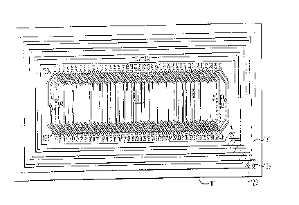
Figure 4a schematically illustrates a sensor head 111
having pick-up windings 133 and 135, each comprising five
periods of series connected alternate sense hexagonal
shaped loops of conductor. In this embodiment, the
period (TS) is equal to 6 mm and winding 135 is quarter
of a period out of phase with winding 133. However, as
will be described in more detail below, the windings 133
and 135 have the same mid points (represented by the
cross in the centre of the windings) on the sensor head
111. The pick-up windings 133 and 135 are formed by
conductive patterns on two sides of a printed circuit
board. The conductors on the top layer are represented
by unbroken lines, whereas those on the bottom layer are
represented by broken lines. The conductors on both
sides of the printed circuit board are connected where
appropriate at via holes 1-46,1'-40',20a and 22a. In
this embodiment, the connection points for connecting the
CA 02238130 1998-OS-15
14
pick-up windings 133 and 135 to the excitation and
processing circuitry (not shown) are provided at vias 20
and 21 for pick-up winding 133 and 22 and 23 for pick-up
winding 135.
As shown in Figure 4a, in this embodiment, the excitation
winding 137 extends around the periphery of the circuit
board from the connection point 123 in a decreasing
clockwise spiral for four turns until via hole X, where
it passes to the other side of the circuit board and then
extends clockwise in an increasing spiral for four turns
to the connection point 125. The connection points 123
and 125 are provided for connecting the excitation
winding 137 to the excitation and processing circuitry
(not shown).
Figure 4b shows the conductive patterns and the via holes
on the top side of the printed circuit board, and Figure
4c shows the conductive patterns and the via holes on the
bottom of the printed circuit board (as viewed from the
top side ) which form the sensor head shown in Figure 4a .
Figures 5a and 5b illustrate the form of each of the two
pick-up windings 133 and 135 respectively. As shown in
Figure 5a, winding 133 comprises a number of hexagonally
shaped loops of series connected conductors, connected
such that adjacent loops are wound in the opposite sense.
Pick-up winding 133 is such that two turns of conductors
are provided for each loop except for the loops at each
end, which only have one turn. In this embodiment, the
repetition period of the loops is matched with the
repetition period of the conductive screens so that the
position of each screen within a period of pick-up
winding 133 is substantially the same.
As shown in Figure 5b, like pick-up winding 133, pick-up
winding 135 also comprises a number of hexagonally shaped
CA 02238130 1998-OS-15
loops of series connected conductors, connected such that
adjacent loops are wound in the opposite sense. As
shown, pick-up winding 135 has two turns of conductor per
loop and has the same total number of hexagonal shaped
5 loops as pick-up winding 133. As shown in Figure 5a and
5b, the mid-point (represented by the cross) of pick-up
winding 133 is substantially the same as the mid-point
of pick-up winding 135. Therefore, if the sensor head
111 tilts relative to the track 101, then the same
10 proportion of each winding will be closer to the track
and the same proportion of each winding will be further
away from the track. Consequently, the signals output
by each pick-up winding 133 and 135 will experience a
similar amplitude change, which will be cancelled out by
15 the ratio-metric calculation performed by the excitation
and processing circuitry (not shown).
As can be seen from Figures 5a and 5b, pick-up winding
133 extends over a greater distance than pick-up winding
135. In order to compensate for this, the hexagonal
shaped loop at each end of pick-up winding 133 is made
less sensitive to magnetic field than the other loops of
pick-up winding 133. In this embodiment, this is
achieved by using only a single turn of conductor to
define the end loops.
In this embodiment, the separation dl is made to be
approximately half the separation dz. This is to make
the pick-up windings 133 and 135 less sensitive to some
of the higher order harmonics of the opposing field
created by the conductive screens 103 which are
energised. This results from the current density which
is induced in the pick-up windings by the opposing
magnetic field.
Figure 6 shows a plot of the current density (J) flowing
in the vertical limbs of one period of one of the pick-up
CA 02238130 1998-OS-15
16
windings shown in Figure 5. From a Fourier analysis of
the current density it can be shown that this current
density can be generated by a fundamental having a period
TS and higher order odd harmonics ( the even harmonics are
zero because of the symmetry) . It can also be shown that
with d2=2d1, the third harmonic content of the current
density is approximately zero. As a result, the pick-up
windings 133 and 135 are sensitive to magnetic fields
which vary periodically along the length of the sensor
head with a period TS, but they are relatively
insensitive to magnetic fields which vary periodically
along the sensor head with a period Tg/3. The
significance of this point will become apparent later.
Figures 7a to 7d illustrate the way in which the multi-
turn pick-up windings 133 and 135 are formed from a
single conductor. The parts of the windings on the top
layer of the printed circuit board are represented by
full lines and those on the bottom layer are represented
by broken lines. As shown in Figure 7a pick-up winding
133 extends from via hole 1 in a generally sinusoidal
manner to via hole 44 at the other end of the sensor
head. Similarly, pick-up winding 135 extends from via
hole 42 in a generally sinusoidal manner along the length
of the sensor head to via hole 46. As shown, the period
of each winding 133 and 135 is TS and winding 135 is
spatially shifted by quarter of a period, i.e. TS/4,
relative to winding 133.
As shown in Figure 7b, pick-up winding 133 extends back
along the sensor head from via hole 44 again following
the same generally sinusoidal path back to via hole 21
which is a connection point for connecting pick-up
winding 133 to the excitation and processing circuitry
(not shown). Pick-up winding 133 continues from the
other connection point at via 20 along the sensor head
in the same generally sinusoidal manner to via 43.
CA 02238130 1998-OS-15
17
Similarly, pick-up winding 135 extends from via 44 back
along the sensor head following the same generally
sinusoidal pattern until it reaches the connection point
at via 23. Pick-up winding 135 continues from the other
connection point at via 22 along the sensor head in the
same sinusoidal manner to via 41.
As shown in Figure 7c, pick-up winding 133 extends from
via 43 back along the length of the sensor head, again
in the same generally sinusoidal manner to via 40'.
Similarly pick-up winding 135 continues from via 41 and
extends back along the sensor head to via 45, again in
the same generally sinusoidal manner. As shown in
Figure 7d, the pick-up windings 133 and 135 extend from
via holes 40' and 45 respectively back along the length
of the sensor head to the starting points at via holes
1 and 42 respectively, as shown in Figure 7a.
Essentially, the inventor has added an extra loop to the
end of one of the windings in order to make their mid-
points coincide. He has also added a second conductor
to some of the loops so that the sensor head is still
relatively immune to background electromagnetic
interference and so that each winding encloses
approximately the same area. To explain further, Figure
8a schematically shows two sensor windings 133' and 135'
having different mid points. Winding 133' has mid point
134 and winding 135' has mid point 136. Figure 8b shows
that by adding the additional loop 138 ( shown in phantom)
to the end of winding 133', that the effective mid point
of winding 133' is now at point 136, ie. the same as that
for winding 135'. Therefore, the windings shown in
Figure 8b will be less sensitive to longitudinal tilt
relative to the track . However, by adding the additional
loop 138 to the end of winding 133' , it becomes sensitive
to background electromagnetic interference since there
are no longer the same number of loops wound in each
CA 02238130 1998-OS-15
18
sense.
In order to overcome this imbalance, a second turn of
conductor is provided for some of the loops in the
windings 133' and 135'. In particular, as shown in
Figure 8c, winding 133' has a second turn of conductor,
represented by the dashed loop 140, for the central loop
and sense winding 135' has a second turn of conductor,
represented by dashed loops 142, for both of its loops.
The additional loops which are added are wound so that
there are equal number of loops wound in each sense, ie.
so that there is an equal numbers of loops wound
clockwise and anticlockwise. The only difference between
the windings 133' and 135' shown in Figure 8c and those
shown in Figures 5a and 5b is that in Figure 8c the
windings extend for only approximately one period,
whereas in Figures 5a and 5b the windings 133 and 135
extend for approximately five periods. The multi-period
design offers the advantages of increased signal strength
and of averaging the signal over a number of periods
which reduces errors due to defects in the manufacture
of the windings and of the track.
In addition to the positional error in the output signal
resulting from the tilt or pitch of the sensor head 111
shown in Figure 1 relative to the track 101, another
positional error arises in the output signal from each
pick-up winding 103 and 105 if the sensor head 111 rolls
about its longitudinal axis. This is because the
conductors which form the pick-up windings are provided
on two sides of a printed circuit board which has a
finite thickness. Therefore, when the sensor head 111
rolls about its longitudinal axis, the cross-over points
between the forward and return conduction paths change.
This results in a perceived positional change along the
x-axis of the sensor head 111 relative to the track 101.
CA 02238130 1998-OS-15
19
The inventor has found that this positional error can be
reduced by, for example, changing the phase of the
conductive windings on each side of the printed circuit
board approximately half-way along the sensor head 111.
This results in the apparent positional change in the
left hand side of the pick-up windings being opposite in
sense to the apparent positional change in the right hand
side. Therefore, the two positional changes cancel each
other out. This positional error can also be minimised
by reducing the thickness of the circuit board.
Figures 9a and 9b show the conductive patterns and the
required via holes on the top and bottom layers of the
printed circuit board respectively to achieve this phase
shift for the pick-up windings 133 and 135 shown in
Figure 4a . As shown in Figure 9a, the conductive patterns
on the left-hand side of the sensor head 111 which were
on the bottom layer of the printed circuit board shown
in Figure 4c, are now on the top layer. Similarly, as
shown in Figure 9b, the conductive patterns on the left-
hand side of the sensor head 111 which were on the top
layer of the printed circuit board shown in Figure 4b,
are now on the bottom layer. A similar compensation can
be made by, for example, notionally splitting the
windings into four quarters and by changing the phase
every quarter.
Due to imperfections in the manufacturing process and the
inability to construct a device having wires which cross
over in the same plane and which are insulated from each
other, positional errors still arise in the output
signals due to tilt and roll of the sensor head 111
relative to the track. Some of these positional errors
can be compensated for by the processing circuitry.
Figure 10 is a block diagram illustrating the processing
circuitry used in the present embodiment. In particular,
the processing circuitry 151 receives the signals 153
CA 02238130 1998-OS-15
from the pick-up windings 133 and 135 as inputs, and
these are fed to the demodulator 155 which outputs
demodulated signals 157. The demodulated signals 157 are
then processed by the compensation unit 159 which
5 compensates for some errors which are inherent in the
system. The compensated output signals 161 from the
compensation unit 159 are then processed by the position
calculation unit 163 which outputs 165 the position of
the sensor head 111 relative to the track 101. Some of
10 the corrections that the compensation unit 159 makes will
now be described in more detail.
One form of error in the signals induced in the pick-up
windings is caused by unwanted cross-coupling between the
15 pick-up windings 133 and 135 and the excitation winding
137. This error is represented by a voltage offset (as
illustrated in Figure 2b) in the demodulated signals 157
output from the demodulator 155. In this embodiment,
this offset is determined by suitable calibration, and
20 is then subtracted from the output demodulated signals
157 by the compensation unit 159.
Another form of error arises when the pick-up windings
133 and 135 have slightly different sensitivities to the
opposing fields generated by the conductive screens 103.
The different sensitivities may arise because of
differences between the areas enclosed by the two
windings 133 and 135. To account for this error, the
compensation unit applies a weighting to one of the
measured output demodulated signals 157. Typically, if
each pick-up winding has the same number of loops, then
the weighting will be approximately 1+0.5~ Additionally,
a phase offset in the demodulated output signals may also
be required if the two pick-up windings 133 and 135 are
not exactly separated by Ts/4. This offset and weighting
can also be determined through suitable calibration.
CA 02238130 1998-OS-15
21
Another form of error which arises in the output signals
is due to variations in the separation between the sensor
head 111 and the track 101. The peak amplitude of the
demodulated output signals decreases when the separation
increases and increases when the separation decreases.
Therefore, a suitable approximate correction value can
be determined by taking a weighted value of the inverse
of the peak amplitude of the output demodulated signals
157. The weighting used also compensates for changes in
the cross coupling interference between the excitation
and pick-up windings which will also change as the
separation changes. Again, this weighting can be
determined by suitable calibration. Since the
demodulated output signals on the pick-up windings 133
and 135 are of the form AsinB and Acos6 respectively
(where A is the peak amplitude and 8 is dependent upon
the position), the peak amplitude (A) can be determined
by squaring the demodulated output voltage from each
pick-up winding, summing the squared values and taking
the square root of the result. In this embodiment, the
compensation unit 159 determines an appropriate
correction value and subtracts this from the demodulated
signals 157.
The inventor has established that without the above
correction values, the output position is typically
accurate to within 2g of the period Ts when the head gap,
i.e. the separation between the sensor head and the
track, is between lmm and 2mm. Whereas, using the
correction values described above, over sensor head gaps
of between lmm and 2mm, with TS equal to 6mm, accuracies
of about 0.1~ TS have been established. Additionally,
the spatial resolution of the position encoder with these
corrections has been demonstrated to be of the order of
0.001 TS.
A number of modifications which can be made to the above
CA 02238130 1998-OS-15
22
embodiments will now be described with reference to
Figures 11 to 14. Figure 11 illustrates an alternative
form of track 101, where the conductive screens 103 have
a rectangular slit 171 in the middle. Preferably, the
dimension WZ shown in Figure 11 should be greater than
the separation between the via holes 1-40 and 1'-40' on
the sensor head 111 shown in Figure 4, as this reduces
the coupling of the magnetic field generated by the
current density on the horizontal limbs of each screen
103 with the windings 133 and 135 on the sensor head 111.
The width d3 of the slit 171 is preferably equal in size
to the separation d4 between adjacent conductive screens
22 and half the width of the vertical limbs 173 of the
screens 103, in order to reduce spatial harmonic
distortion. More specifically, when the conductive
screens opposite the sensor head are energised by a
current flowing in the excitation winding, a surface
current density is generated on the screens which
generates an opposing magnetic field which varies
periodically with position along the track.
Figure 12a shows the resultant current surface density
flowing in the vertical limbs 173 of two adjacent
conductive screens 103, ignoring the current density in
the horizontal limbs. Since several adjacent conductive
screens 103 are energised together, the opposing magnetic
field (Hy) generated by the conductive screens 103 will
be periodic and, at the surface of the screens 103, will
have the form generally shown in Figure 12b. It can be
shown from a Fourier analysis of the signal shown in
Figure 12b, that this signal contains a fundamental
component having a spatial period Ts and higher order
harmonics, and that by making d3 and d4 equal to 1/6 of
the period TS, there is no second or third harmonic
content. The significance of this will now be explained.
The magnetic field generated by the conductive screens
CA 02238130 1998-OS-15
23
decays exponentially with distance from the surface of
the screens. Since the higher order harmonics have a
lower amplitude at the surface of the screens, these
components die off more quickly than, for example, the
fundamental component. Therefore, if the sensor head is
operated at a distance of approximately lmm or 2mm from
the surface of the track, then most of the opposing
magnetic field coupling with the pick-up windings 133 and
135 will be due to the lower order harmonics. However,
by providing a rectangular slit 24 in the middle of the
conductive screens with the dimensions described above,
only the fundamental component of the opposing magnetic
field will dominate at the surface of the sensor head
111.
This embodiment has a manufacturing cost equal to that
of the first embodiment, when using printed circuit board
construction techniques. Additionally, the input current
to output voltage phase relationship will be similar to
that of the first embodiment.
Figure 13a illustrates a preferred form of track 101
where the conductive screens are replaced by resonant
circuits 181. As in the first embodiment, the repetition
period of the resonant circuits 181 is the same as the
spatial period TS of the pick-up windings. By using
resonant circuits 181, it is possible to use a pulse-echo
mode of operation, whereby short bursts of excitation
current are applied at the resonant frequency of the
resonators 181, and the processing circuitry processes
the signals induced in the pick-up windings after the
excitation current has been removed. This mode of
operation works because the resonators 181 continue to
"ring" for a short period of time after the burst of
excitation current has been removed. This mode of
operation eliminates possible cross-coupling between the
excitation windings and the pick-up windings.
CA 02238130 1998-OS-15
24
As shown in Figure 13a, each resonant circuit 181 of this
embodiment comprises a coil 183 and a capacitor 185. One
end of the coil 183 is connected to an end of the
capacitor 185 and extends away from the capacitor
following an anticlockwise reducing spiral path until it
reaches the via hole 187. At via hole 187 the coil 183
passes through to the other side of the track 101 and
continues in an enlarging spiral winding until it reaches
via hole 189, where it passes back through the board and
connects to the other end of the capacitor 185. In this
embodiment the capacitor is a surface mount capacitor,
using NPO dielectric with a value of 5.6 nF, which is
mounted on one side of the printed circuit board having
a thickness of approximately 0.4mm. The dimension WZ
shown in Figure 13a should be greater than the separation
between opposing via holes 1-40 and 1'-40' shown in
Figure 4, as this reduces the unwanted effects of the
current flowing in the horizontal conductors of the
coils. In this embodiment, the separation between
opposing via holes is 6mm and the dimension W2 is 8mm.
The height H of the coil 183 in this embodiment, is 13mm.
As in the embodiment shown in Figure 11, the widths d3
and d4 are preferably equal to approximately 1/6 of the
period TS, as this reduces the unwanted 2nd and 3rd
spatial harmonics of the magnetic field produced by the
resonators 181.
Figure 13b, the top copper layer, shows the reducing
anticlockwise spiral winding of coil 183. Figure 13c,
the bottom copper layer (as viewed from the top copper
layer), shows the enlarging anticlockwise spiral winding
of coil 183.
As is well known in the art, the Q of a resonant circuit
is dependent upon the area of copper which forms the
coil, for a given copper foil thickness. The use of a
multi-turn coil on both sides of the track 101 is
CA 02238130 1998-OS-15
consistent with maintaining a high Q and reasonable
impedance levels. Preferably, high stability capacitors
are used with the multi-turn coils 183 in the resonator
design. Embodiments with one or two turns are envisaged,
5 but capacitors having the required values and stability
are not manufactured presently.
In the resonator embodiment, with a typical drive current
of approximately 100 mA, at a frequency of approximately
10 1 MHz, and with a separation between the sensor head 111
and the track 101 of approximately lmm, the voltage
induced in the pick-up windings will be approximately 100
mV rms . However, as the separation increases, the output
voltage reduces exponentially. For example, at a
15 separation of 2mm the voltage output from the pick-up
windings is approximately 30 mV rms.
As mentioned above, the advantage of using resonant
circuits as the passive elements on the track 101, is
20 that the system can be operated in a pulse-echo mode of
operation. However, since the impedance of the resonant
circuits 181 at resonance is purely resistive, there is
a well defined phase relationship between the excitation
current and the voltage induced in the pick-up windings.
25 Therefore, even if the excitation current is continuously
applied to the excitation winding, the processing
circuitry (not shown) will be able to differentiate
between the signals induced in the pick-up windings by
the resonators from the signal induced in the pick-up
windings by the excitation winding. In particular, when
resonant circuits are used, the phase of the synchronous
detector is set to give the minimum cross-coupling offset
error.
Figure 14 illustrates an alternative embodiment, where
the track 101 carries a plurality of short circuit coils
183 in place of the conductive screens 103. Again, the
CA 02238130 1998-OS-15
26
repetition period of the short circuit coils 183 is set
to be equal to the spatial period TS of the pick-up
windings. This embodiment operates in a similar manner
to the embodiment described above with reference to
Figure 11. This embodiment is slightly cheaper to
implement than the resonant circuit embodiment as there
is no capacitor. The dimensions of the coils 183 in this
embodiment are the same as those of the coils shown in
Figure 13a.
Although sinusoidal and hexagonal shaped pick-up windings
have been shown in the drawings, alternative geometries
or patterns of conductors could be used. For example,
square-wave or triangular-wave windings and any other
three piecewise linear approximations.
Although two-phase quadrature pick-up windings have been
employed on the sensor head 111, in the above
embodiments, a sensor head employing three, four or any
number of suitably shifted pick-up windings could be
used. For example, three pick-up windings could be
provided on the sensor head, each spatially separated
from the other by TS/6.
The operating frequency of the encoder is mainly
determined by physical size and the required circuit
impedances. Typically, the operating frequency ranges
from 10 KHz to 10 MHz, with 300 KHz being optimal for the
six millimetre pitch pick-up windings and conductive
screens. The optimum operating frequency when resonators
are used is dependent upon the resonator Q, but will
typically be about lMHz. In the resonator design, the
required circuit impedance can be obtained by using
series or parallel connected resonating capacitors if
required. Alternatively, impedance electrical
transformers can be utilised which have the added
advantages of introducing galvanic isolation, suppressing
CA 02238130 1998-OS-15
27
common mode interference signals and improving the power
efficiency of the sensor.
The inventor believes that by using these correcting
techniques, it is possible to scale the device over a
very large range of pick-up winding period TS. For
example, it is envisaged that the sensor head could be
implemented on silicon. In this case, it would be
possible to implement the entire sensor head including
the processing circuitry, on a single integrated circuit
chip.
Furthermore, it is possible to shield the position
encoder system from surrounding electromagnetic
interference, thereby allowing the device to be used in
electromagnetically hostile environments. In addition,
the system is not adversely affected if a steel backing
plate is provided behind the track 101 and/or if a thin
stainless steel (i.e. non-magnetic) layer is placed over
the track. However, when such a stainless steel cover
is used, the operating frequency must be sufficiently
high to make the stainless steel seem transparent to the
generated magnetic fields. Therefore, the system can be
used in a wide variety of applications, including high
accuracy industrial applications, such as machine tool
position sensing.
It is also envisaged that the track 101 could be formed
into a circular ring, thereby providing a rotary position
sensor.
The present invention is not intended to be limited by
the exemplary embodiments described above, and various
other modifications and embodiments will be apparent to
those skilled in the art.