Note: Descriptions are shown in the official language in which they were submitted.
CA 02238192 1998-05-20
W~97119541 PCT/SE96/01485
FILTERING IN A RECEIVER THAT USES
LO&-POLAR SIGNAL P~OCESSING
BACKGROUND
The present invention relates to filtering of radio
fre~uency signals, and more particularly to digital
techniques for filtering radio frequency signals that are
supplied in ~og-polar format.
In the telecommunications arts, such as in mobile
telephony, it is known that it is always possible to
represent an arbitrary radio signal as a sequence of
composite (complex~ vectors. Thus, a radio signal can be
expressed either in Cartesian (I, Q) form or in polar
(RSS, PHI) form, where RSS is the received signal
strength, and PHI represents the phase angle of the
vector. It is also known thLat a so-called "log polar
form" can be advantageously used as an alternative to the
two forms mentioned above.
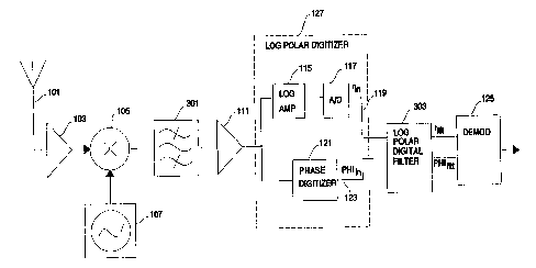
FIG. 1 is a block diagram of a conventional log polar
receiver. A radio signal is received by an antenna 101
and supplied to an amplifier 103. The ampli~ied signal is
then supplied to a mixer 105, where it is mixed with a
signal generated by a local oscillator 107 to produce a
signal having a suitable intermediate ~requency ("I.F.
signal"). The I.F. signal is then supplied to a bandpass
filter whose purpose is to p~ss only those frequencies
that lie within the range of a bandwidth centered around
a predefined center frequency.
After further amplification by amplifier 111, the
analog I.F. signal 113 is supplied to a log polar
digitizer 127. In a first leg of the log polar digitizer
127, the analog I.F. signa] 113 is amplified by a
logarithmic amplifier 115 and then converted to a digital
form by the analog-to-digital (A/D) converter 117. Each
output of the A/D converter 117 represents the log of the
received signal strength (rss 119) at a particular instant
WO 97/1 9S4 1 CA O 2 2 3 8 19 2 19 9 8 - O ~ - 2 0 PCT/SE96/01485
in time.
In another leg of the log polar digitizer 17, the
analog I.F. signal 113 is supplied to a phase digitizer
121, which generates a digital signal, PHI 123, which
represents the phase of the applied analog I.F. signal
113.
The digital signals rss 119 and PHI 123, which are
generated by the log polar digitizer 127, are then
supplied to a demodulator 125 which processes these
signals using known digital techniques to generate a
demodulated signal.
The performance of the bandpass filter 109 is
important because it determines the extent to which the
receiver will respond to all frequencies within the
defined channel, and reject (i.e., not respond to) all
frequencies falling outside the channel. FIG. 2 is a
graph of the frequency characteristics of the bandpass
filter 109. The bandpass filter 109 is designed to pass
only those frequency components of the input signal that
lie in the range from fCENTER A to fCENTE~ B- In the
illustrated example, fCENTE~s selected to be a desired
I.F. for the receiver circuit.
In the conventional receiver, the bandpass filter 109
is constructed entirely from analog components. This
introduces a number of problems due to imperfections and
variations of components during construction as well as
variations that arise as a result of aging of the
components. For example, referring to FIG. 2, the
filter's bandwidth, A + B, may be too wide. This results
in signals from adjacent channels being passed on to the
demodulator. Or, the filter's bandwidth, A + B, may be
too narrow. This results in loss of performance at the
desired channel due to parts of the desired signal being
removed. Also, it is possible that the center frequency,
fCENTERis incorrect, so that A ] B. In this case, parts
CA 02238192 1998-05-20
W O 47/195~1 PCT/SE96/~1485
of the desired signal will be removed and parts of an
adjacent channel will be introduced.
SUMM~RY
In accordance with one. aspect of the present
invention, the foregoing and ot:her objects are achieved in
a log polar digital filter for processing a digitized log
polar signal that comprises a logarithmically-scaled
magnitude signal (rin~and an angle signal ~PHIin). In one
embodiment, the log polar digi.tal filter comprises first
conversion means for converting the log polar signal into
a converted linear Cartesian signal, wherein the converted
linear Cartesian signal comprises an in-phase signal (Iin)
and a quadrature signal (Qin).I'he log polar digital filter
further comprises a digital fi:Lter, referred to here as a
linear cartesian digital filter, that is coupled to the
first conversion means, for generating a filtered linear
Cartesian signal from the converted linear Cartesian
signal. The linear Cartesian signal comprises an in-phase
signal and a quadrature-phase signal.
In another aspect of the invention, the log polar
digital filter further comprises an analog circuit for
generating an analog signal, and a log polar digitizer for
- generating the digitized log polar signal from the analog
signal. The first conversion means generates the
converted linear Cartesian sig:nal in accordance with the
equations:
b (rln-~ffs-tin) ( PHI
and
Q b k fn-~ f fsetin) i (PHI
CA 02238192 1998-0~-20
W O 97/19541 PCT/SE96/~1485
where binand offsetinare calibration constants. These
calibration constants may be used to adapt the
linearization of the characteristics of the log polar
digitizer and to compensate for gain errors introduced in
the analog circuit. The analog circuit may include, for
example, an analog bandpass filter; and an analog
amplifier, coupled to receive a filtered signal from the
analog bandpass filter.
In another aspect of the invention, the linear
Cartesian digital filter compensates for out-of-
specification operation of the analog circuit.
In still another aspect of the invention, the log
polar digital filter further comprises second conversion
means, coupled to the linear Cartesian digital filter, for
~5 converting the filtered linear Cartesian signal into a
filtered log polar signal, the filtered log polar signal
comprising a filtered magnitude signal (rfil~d a filtered
angle signal (PHI~ilt)-
The log polar digital filter may still further
comprise third means for further processing the filteredlog polar signal. The second conversion means in this
case may generate the filtered log polar signal in
accordance with the equations:
rfilt = 1 g bilC + offset
and
PHIfilC = arg(Ifilt + jQfilt)
where arg() denotes the argument of a complex number,
r/ilt =~Ifilt ~ Qfilt / and bou~nd offsetou~re constants that
-
CA 02238192 1998-05-20
WO~7/19541 PCT/SE9~0148S
may be selected to cause the filtered log polar signal to
satisfy range and resolution requirements of the third
means.
In another embodiment oi- the invention, the first
conversion means generates the converted linear Cartesian
signal in accordance with the equations:
b~rin~~ff~ePtin) * COS (PHIin+2~fcorrt)
and
p b (rin-offS~tin) * s~ (PHI +2 f t)
where bi~nd offsetinare calibration constants that may be
used to adapt the linearization to the characteristics of
the log polar digitizer and to compensate for gain errors
introduced in the analog circuit, t is a time stamp of a
current sample, and fcor~S a frequency constant for
correcting for asymmetrical frequency characteristics of
the analog circuit. Also, the second means generates the
filtered log polar signal in accordance with the
equations:
rfilt = l~g b + Offsetout
and
PHIfil t = ( arg (If il t + iQfilt) - 2~fcorr t) modulo 2 7~
where rfi1t = ~Ifilt +Q2ilt, and b_out and offsetOutare
constants that may ~e selected to cause the filtered log
polar signal to satisfy range and resolution requirements
WO97/19541 CA 02238l92 l998-05-20 PCT/S~96/01485
of the third means. The constant fcor~ay be selected to
cause the linear Cartesian digital filter to move in
frequency so as to compensate for badly centered analog
filter characteristics.
5BRIEF DESCRIPTION OF THE DRAWINGS
The objects and advantages of the invention will be
understood by reading the following detailed description
in conjunction with the drawings in which:
FIG. 1 is a block diagram of a conventional log polar
receiver;
FIG. 2 is a graph of the frequency characteristics of
a bandpass filter;
FIG. 3 is a block diagram of an exemplary log polar
receiver in accordance with one aspect of the invention;
and
FIG. 4 is a block diagram of an exemplary embodiment
of the log polar digital filter in accordance with the
invention.
DETAILED DESCRIPTION
20The various features of the invention will now be
described with respect to the figures, in which like parts
are identified with the same reference characters.
FIG. 3 is a block diagram of an exemplary log polar
receiver in accordance with one aspect of the invention.
25The antenna 101, amplifiers 103 and 111, mixer 105, local
oscillator 107, logarithmic amplifier 115, A/D conver~er
117, phase digitizer 121 and demodulator 125 operate the
same as those described above with respect to FIG. 1, so
no additional description is necessary. In a preferred
embodiment, the log polar digitizer 127 is that which is
described in greater detail in U.S. Patent No. 5,048,059
to P. Dent, which is incorporated herein by reference.
The function of the bandpass filter 301 is the same
CA 02238192 1998-0~-20
WO97119541 PCTISE96/01485
as that of the bandpass filter lO9 described above.
However, in accordance with one aspect of the invention,
the bandpass filter 301 need 1~ot operate under the same
exacting standards as that oi- the bandpass filter lO9
because of the addition of a log polar digital filter 303,
by which is meant means that utilize digital techniques to
filter a digitized log polar signal. The coefficients of
the log polar digital filter 303 are prefera~ly loadable,
so that different sets may be 1lsed for:
l) compensating for different filter characteristics
of the analog parts of the receiver. For example, if the
bandwidth (A+B; see FIG. 2) of the bandpass ~ilter 301 is
too wide, then coefficients for the log polar digital
filter 303 should be select:ed to produce a narrow
bandwidth that, when following the bandpass filter 301,
will produce the desired band~idth. Similarly, if the
bandwidth (A+B; see FIG. 2) of the bandpass filter 301 is
too narrow, then coefficients for the log polar digital
filter 303 should be selected to produce a wider bandwidth
that, when following the bandpass filter 301, will produce
the desired bandwidth.
23 compensating for a bandpass filter 301 that is
not symmetrical, that is, one whose center frequency
- (fcENTER;see FIG. 2) is not actually on the desired
intermediate frequency ~I.F.).
3) ad~usting the total filter characteristics of the
circuit to satisfy the overall requirements of the
application.
Techniques for making the above-described
compensations and adjustments are described in greater
detail below.
It will be observed that the log polar digital filter
303 is required to process signals that are in log polar
form. In accordance with another aspect of the invention,
the log polar digital filter 303 has this capability. An
WO97119541 CA 02238192 199X-05-20 PCT/SE96/01485
exemplary embodiment of the log polar digital filter 303
will now be described with respect to FIG. 4.
Within the exemplary log polar digital filter 303,
the log polar signals to be processed ~i.e., the digital
signals rinll9 and PHIinl23) are supplied to means for
converting signals from log polar form into Cartesian
form. Such means, depicted in FIG. 4 as the log polar-
to-Cartesian converter 401, may be implemented, for
example, as an application specific integrated circuit
(ASIC) or other hardwired circuit, or alternatively as
software running on a programmable device. In either
case, the log polar-to-Cartesian converter 401 generally
operates in accordance with the following equations in
order to generate the linear Cartesian form input signals,
Iin403 and Qin405, from the log polar signals rinll9 and
PHIinl23:
b~riA-offsetln) * cos (P~Iin) = r~ * cos (PHlin)
(1)
p b(rin~~ffsetin~ * Sin(PHIin) = r~ * sin(P~Iin)
~2)
where binand offsetinare calibration constants that may be
used to adapt the linearization to the characteristics of
the log polar digitizer 127 and to compensate for gain and
offset errors that may arise due to imperfections and
variations in the analog parts of the radio.
In one embodiment, the signal ri~l9 comprises lO-bit
samples (capable of representing values in the range from
0 to 1023), and PHIinl23 comprises 8-bit samples in the
range from 0 to 255. Since Equations (l) and (2) above
assume that the phase value is in radians, these equations
must be slightly modified as follows, in order to
accommodate the 8-bit representation of PHlinl23:
I in = b in(r in-offset in) * cos (2.pi.PHI in/256) = r~in*cos(2.pi.*PHI in/256
(1')
Q in = b in(r in-offset in) * sin(2.pi.*PHI in/256) = r~in*sin(2.pi.*PHI in/256
(2')
where
r~in = b in(r in - offset in) (3)
In one embodiment, the constants b in and offset in are
preferably stored in registers within the log polar-to-Cartesian
converter 401, so that they may be software
loadable.
It is noted that values for r'in may be computed from
equation (3) by means of fixed point arithmetic. However,
when floating point arithmetic is utilized, the
determination of values for r'in may be made more efficient
by means of the following technique in accordance with
another aspect of the invention. First, it is noted that
r~in = b in(r in -offset in) = 2 (-(offset in-r in)*log2bin)
(4)
In floating point arithmetic, each value is
represented in the form: mantissa * 2exponent Consequently,
equation (4) leads to the following formula for
determining the linear value r'in:
r~in= 2(-integer((r'in+(-offset in))*(-log2b in) - frac((r in+(-offset in))*(-log2b in)))
= 2(exponent)*2(-frac((r in+(-offset in))*(-log2b in)) (5)
CA 02238192 1998-0~-20
W O 97/19541 PCT/SE96/01485
The last exponential in equation (5), that is the
expression ~-frac((rlnl~-offgetfn))~ ogz~in))) ~may be computed by
letting x = frac((rin+(-offsetin))*(-log2bin~ applying
a Tschebyscheff expansion for the function 2 X,namely:
P ( X) = C7 *X7 + ... + Cl*xl + CO *X~ ( 6 )
The coefficients C7, C6, . . . , C1, C0 are the polynomial
coefficients in a Tschebyscheff expansion, and should be
selected to provide good results for the expected range of
values of rin. Although eight terms are illustrated, the
number of terms in the polynomial depends on the level of
accuracy that is required for the given application.
It can be seen that the operation of the log polar-
to-Cartesian converter 401 depends on the values that are
selected for binand of~setin In yet another aspect of the
invention, these values may be selected as a function of
the radio dynamics as follows: First, the variable r'inis
written as a function of the signal rinll9:
rln ( rin) = bin
(7)
.
Expressing r'inin decibels (dB), we get:
r~(rin) = 20* (rin~~ffSetin) *l~glObin (8)
Taking the derivative o~ both sides and rearranging
variables yields the following expressions for binand
log2bin:
CA 02238192 1998-05-20
W O g7119541 PCT/S~96/~1485
dB) = 20*1~globin
d kin)
d(r~
b = lO d(l~n)~20
d ( IdB) *1~g21~
~g2bi~ = d(Iin) *20
~9)
where d~ ~ is the signal st:rength of r (in dB) per rin
step. This value may be deter:mined empirically for each
radio unit by making measurements during production, using
well-known techniques.
Having determined a suit:able value for bin (and,
therefore, log2bin as well), one can determine a
corresponding value for offsetinas follows:
ri ( ~ ) = b0n0ffS6~ in
r~ = -20*offsetin*l~glObin
rdB(~) -r~(O)*log210
in 2o*loglcbin 20*10g2~in
. (10)
Thus, in a preferred embodiment, values for -log2b
and -offsetinare predetermined for a given log polar-to-
Cartesian converter 401, and these values are programmed
into a memory means located in the log polar-to-Cartesian
. converter 401. During operat:ion of the log polar-to-
Cartesian converter 401, equation (5) is used to determine
~ a value for rinfrom the pre-st:ored values of -log2bi~nd
-offsetinand from the input va].ues of the signal rinll9.
The cosine and sine of the phase (see equations (1')
and (2')) may be determined in accordance with well-known
CA 02238192 1998-0~-20
W O 97/19~41 PCT/SE96/01485
table-lookup techniques. However, in another embodiment,
the cosine of the phase is computed by applying a
Tschebyscheff expansion of the function costpi*x) to a
suitable normalization of the phase. Mathematically,
cOs ( 2*lC*PHIin/256) = -COS(~*( PHIin-128) /128)
and the polynomial
P (X) = C5 *x10 + C4 *X8 + , . . + Co *X~
is applied to ((PHIin-128)/128)).
The computation of the imaginary part is entirely
analogous; sin(pi*x) is approximated by the polynomial
P ~ x) = x ( K4 *X8 + K3 *X6 + , . . + Ko *x~ )
The coefficients for the polynomial expressions
should be determined to provide good approximations for
the expected range of input values. Techniques for
selecting coefficients to satisfy the criterion are well
known in the art. Also, when PHIinequals 0, 64 or 192
(i.e., those angles that should have zero cos or sin
values, but which generate non-zero values when the
polynomial is computed), the log polar-to-Cartesian
converter 401 may skip the step of evaluating the
polynomial, and instead merely use the accurate answer of
~ero.
Referring back to FIG. 4, the log polar digital
filter 303 further includes a digital filter, henceforth
referred to throughout this specification as a linear
Cartesian digital filter 407 that receives the Iinand Qin
signals 403 and 405 that are generated by the log polar-
to-Cartesian converter 401, and generates therefrom
filtered signals Ifi~9 and Qfi~1. The linear Cartesian
CA 02238192 1998-0~-20
W O ~7/19541 ~CTJS~96/014~5
13
digital filter 407 may be any type of digital filter
(e.g., finite impulse response (FIR) or infinite impulse
response (IIR)) that meets the requirements o~ the
receiver. one aspect of the linear Cartesian digital
filter 407 is that it may have two independent filter
paths, so that the signals lin403 and Qin405 may be
processed separately. Technilques for designing linear
Cartesian digital filters are well-known in the art, and
are application specific. Accordingly, a more detailed
description of the linear Cartesian digital filter 407 is
beyond the scope of the invent:Lon.
In one aspect of the invention, the coefficients of
the linear Cartesian digital filter 407 are loadable, and
different sets of coefficients may be used to compensate
for out-of-specification filter characteristics of the
analog parts of the radio. The term "out-of-specification
operation" is used here to mean actual operation that is
not in accordance with the intended operation. As
explained in the BACKGROUND section of this specification,
although two different analog circuits may be built with
the same nominal components, imperfections and variations
of components during construction, as well as variations
that arise as a result of aging of the components, will
-- cause the circuits to exhibit d:ifferent characteristics in
operation.
one example of compensation that the linear Cartesian
digital filter 407 can provide is illustrated by the case
where the bandwidth of the bandpass filter 301 is found to
be too wide. In this instance, the coefficients of the
linear Cartesian digital filter 407 may be selected to
effect a bandpass filter having a narrow bandwidth, so
that the sum total of ~iltering satisfies the requirements
of the specification. Similarly, if the bandwidth of the
bandpass filter 301 is found to be too narrow, then
coefficients of the linear Cartesian digital filter 407
WO97/19541 CA 02238192 1998-0~-20 PCT/SE96/01485
14
may be selected to effect a bandpass filter having a wide
bandwidth. In each case, the net effect of the series
connected filters should produce the desired filtering
that would otherwise be performed by the analog bandpass
filter 301 alone.
The coefficients of the linear Cartesian digital
filter 407 may further be selected to ad~ust the total
filter characteristics so as to satisfy the total filter
characteristics of the intended application (in this case,
a receiver). In this case, coefficients are selected by
considering not only the actual performance of the analog
bandpass filter 301, but also the performance of filters
that receive signals derived from the output of the linear
Cartesian digital filter 407.
By making the coefficients of the linear cartesian
digital filter 407 software loadable, different sets of
coefficients may be used for different applications. ~or
example, one set may be loaded for an application
re~uiring high adjacent channel rejection, while another
set may be utilized if no adjacent channel interferers are
present.
The filtered signals Ifil~09 and Qfil~ll that are
generated by the linear Cartesian digital filter 407 may,
in some embodiments, be directly supplied to other
components in the receiver for further processing. In the
illustrative embodiment, however, it is necessary for
these signals to first ~e converted back into log polar
form before they can be supplied to other components in
the receiver. Consequently, the log polar digital filter
303 further includes means for converting Cartesian form
signals into log polar form. Such means may be
alternatively constructed in a number of different ways,
including as an ASIC or as a general purpose processor
running a conversion program. The conversion means are
3s represented in FIG. 4 as the Cartesian-to-log polar
CA 02238192 1998-05-20
W O 97/19541 PCT/SE96/V1485
converter 413, which receives the filtered signals Ifi~9
and Qfi~l, and generates therefrom the filtered signals
rfi~5 and PHIfi~7.
The filtered phase signal PHIfi~7 may be determined
in accordance with the equation
PHIfilt = arg(Ifil~ + iQfilt) ( ll)
where arg() denotes the argument of a complex number.
A filtered magnitude signal may also be determined in
accordance with a well known linear-to-log polar
conversion algorithm. However, in accordance with another
aspect of the invention, the Cartesian-to-log polar
converter 413 not only converts the filtered signals, Ifilt
409 and Qfi~l, into log polar form, but may also scale
the filtered signals, rfi~5 and PHIfi~7, so that they
will have a resolution and range suitable for the signal
processing that follows (e.g., a Viterbi equalizer). This
scaling may be accomplished by adjusting the filtered
signal rfi~5 in accordance with the equation:
rfilt = b~uef~lc~~ffSeeou~)
(12)
where rfilt = ~Ifile + Qfile is a linearly scaled polar
magnitude value, and bOu~nd offsetOu~re constants that are
preferably capable of being loaded into the Cartesian-to-
log polar converter 413 by means of a software download
operation.
In accordance with yet another aspect of the
invention, the Cartesian-to-log polar converter 413 is
designed to efficiently conver1 and scale the filtered
CA 02238192 1998-05-20
W O 97/19541 PCT/SE96/01485
16
signal by taking advantage of the fact that the filtered
signals, I~ 9 and Qfi~l, are preferably represented in
a ~loating point format. It follows from equation (12)
that
rfilt = l~gbou~rfil~+~ffSetout
2 logbout (Ifilt*Ifilt+Qfil~*Q~ilt) +offse tout
(Ifil t*Ifil t+Qfil t *Qfil t) +o f f se tout
2 ~g2 Oue
= K*l~g2 (Ifilt*Ifil~ +Qfilt*pfilt) +offse~Out (13)
It is observed that, in a preferred embodiment, Ifilt
and Qfi~e represented in floating point format, so that
Ifilt*I~ilt+Pfilt*Qfilt = m*2 (14)
where m is a mantissa in the range 1~m<1 , and exponent
is represented as an integer value. It follows, then,
that
~ga (Ifilt*Ifilt+Qfilt*Qfilt~ = 1~g2 (m*2eXPonent) = log2m + expon,
(15)
In a preferred embodiment, log2 m is approximated by
P(2*(1-m)),where
P (x) = Clo *X10 + . . . + Cl *Xl + co *x~
15 The coefficients c10,... , cl, cQ should ~e selected in
accordance with known techniques to optimize the
polynomial expansion to give a good approximation for the
expected range of input values.
,
CA 02238192 1998-05-20
W ~97~19541 PCT/SE96/01485
A value for K may be selected for use in equation
(13) by solving equation (12) for bout
d ( r2~
b = 10 d(rf~ 2~ (16)
where, d( ~ ) is a desired signal strength of r (in dB~
per rfi~ep.
It follows from equation (16) that
1 o~ b = d ( r~) *logzlO
(17)
The constant K can now be calculated as:
K = 1 = 10
2*logzbout log 10*( d(r~) )
(18)
Having determined a value for K, a value for offsetOut
can be calculated as:
offsetOu~ = rfilt - logl~Ou2rfilt
= r log2rfilt
fil t lO~2boue
= rfilt - 2 ~K~l~g2rfilt
= rfilt - 2*K~l~g2 ~/Ifilt + Pfilt (19)
In a preferred embodiment, the constants K and
offsetOutare software loadable into the Cartesian-to-log
polar converter ~13.
CA 02238192 1998-0~-20
W O 97/19541 PCT/SE96/01485
18
In another aspect of the invention, the filtered
signal PHIfi~7 is generated from the filtered signals, ~filt
409 and Qfi~1, by first reducing these values to the case
where both Ifi~d Qfi~e positive, with Qfi~ing less than
or equal to Ifilt'rhen, the ratio Ifilt is supplied as an
fil ~
input to a polynomial approximation of the function arctan
(x), thereby yielding a value for PHIfilt~odulo the
reduction made to bring Ifi~d Qfi ~to the desired range.
Conse~uently, the value for P~Ifil~ust be adjusted to
produce an accurate filtered signal PHIf~ 7. The
polynomial approximation that is used is preferably of
degree 7.
When utilizing the log polar digital filter 303 to
compensate for variations of the characteristics of the
analog bandpass filter 301 (and/or any other filters that
may be present, depending on the application), it becomes
apparent that the analog filters are not symmetrical.
That is, the actual center fre~uency for filtering is not
the desired center frequency. In accordance with another
aspect of the invention, this problem is corrected by
introducing an intentional frequency offset in the log
~ polar-to-Cartesian converter 4~1 and in the Cartesian-to-
log polar converter 413.
More specifically, the log polar-to-Cartesian
converter 401 is, in this case, designed to perform its
conversion in accordance with the following relationships:
b (rin-offSetin) *COS( PHIin+2 ~c fcorr t)
(20)
and
CA 02238192 1998-05-20
WO97/19541 PCT/SE96/01485
19
Q b ~ in-offsetin) *sirl ( pHIin+27~ fcorrt)
(21)
where rin,offsetin binand PHIinare the same as described
above (with PHIinassumed to be expressed in radians).
Similarly, the Cartesian-to-log polar converter 413
is designed to perform its conversion in accordance with
the following relationships:
rfilt =K*10g2 ~Ifilt + Pfilt) + offsetO"t (22)
and
PHIfil t = ( arg ( II~il t + jQfil t l - 2 ~ fco~ r t ) modul o 2 ~ ( 2 3 )
In this case, the only difference in operation from that
which has been previously described is the introduction of
the compensation factor, 2~ fco~rt ~ where fCorris the
correction frequency, and t is the time stamp of the
current sample.
A suitable value for fco~Y be empirically determined
by supplying the log polar digital filter 303 with a
signal having the same bandwidth and center frequency that
will be used when the system is later used in the field.
The parameter fCor~s then adjusted to maximize the output
20 signal, rfilt-
The invention has been descrlbed with reference to aparticular embodiment. However, it will be readily
apparent to those skilled in the art that it is possible
to embody the invention in specific forms other than those
of the preferred embodiment described above. This may be
done without departing from the spirit of the invention.
For example, in the illustrative embodiments, the log
WOg7/19541 CA 02238192 1998-05-20 PCT~E96/01485
polar signals were received radio signals having received
signal strength and phase components. However, the
invention is not limited to this embodiment, but rather
may be applied for filtering any type of log polar signal,
that i5, one comprising a magnitude signal and an angle
signal, with the magnitude signal being scaled
logarithmically.
Thus, the preferred embodiment is merely illustrative
and should not be considered restrictive in any way. The
scope of the invention is given by the appended claims,
rather than the preceding description, and all variations
and equivalents which fall within the range of the claims
are intended to be embraced therein.