Note: Descriptions are shown in the official language in which they were submitted.
CA 02238332 2002-06-20
WO 97/19540 PCT/SE96/01486
1
Determining Signal Components Using Digital Signal Processing
BACKGROUNla
The present invention is directed generally to radiocommunication systems
and, more particularly, to techniques for determining sine and cosine values
to
facilitate modulation of a signal for radio transmission.
The first cellular mobile radio systems utilized analog systems to process
and convey speech and other analog information. These systems comprised
multiple radio channels for transmitting analog information between base and
mobile stations by transmitting analob modulated radio signals. In general,
the
signal handling processes in such systems were performed by analog hardware in
the base and mobile stations.
Recently, digital cellular mobile radio systems for public use have been
designed. Digital cellular mobile radio systems utilize digital signal
processing
and digital radio channels for handling digital or digitized analog
information
transmitted between base and mobile stations. Digital cellular mobile radio
systems may offer substantial advantages, e.g., increased system capacity,
reduced component size and enhanced signal processing capability, over analog
cellular mobile radio systems. To achieve these advantages there are certain
demands on. the digital signal processing. In particular, signal handling
processes
need to be performed rapidly and frequently relative to conventional analog
systems.
In contrast to the introduction of digital-only cellular mobile radio
systems, in areas with existing analog cellular systems it has been proposed
to
introduce digital cellular mobile radio systems which are designed to
accommodate existing analog cellular mobile radio systems. In this way, large
legacy customer bases will not suddenly find that their analog terminal
equipment
has become obsolete. System designers of these hybrid systems believe that the
digital portion of the system can be gradually introduced and, over time, the
CA 02238332 1998-OS-22
WO 97/19540 PCT/SE96/01486
2
number of digital channels can be gradually increased, while the number of
analog channels is gradually decreased. In order to provide complete
compatibility, such dual-mode systems should comport with both analog and ,
digital standards that have been adopted. Because a large number of analog
mobile stations remain in use, digital base stations must be able to support
communication with those analog units as well as new digital units.
In an analog cellular system, information (source signals), can be
conveyed in the form of frequency modulated {FM) modulated signals. An FM
modulator encodes the analog source signals onto a Garner signal to generate a
modulated signal. The modulated signal is then transmitted. A conventional FM
modulator is depicted in Figure I. An analog source signal 100 is provided to
an
input port of a mixer 102. A carrier signal 105, generated by a voltage
controlled oscillator (VCO) 104, is provided to a second input port of the
mixer
102. The VCO can be tuned to a frequency associated with a channel that has
been allocated for a particular transmission. The output of the mixer 102 is a
modulated signal 106 having a frequency of the carrier signal I05 and
containing
the information in the source signal 100. The modulated signal 106 is
transmitted by a radio 108.
Frequency modulation was adopted to overcome shortcomings inherent in
amplitude modulated {AM) radio systems. AM signals carry information in the
form of amplitude variations. However, such a modulation scheme is inherently
susceptible to noise, fade and interference problems. FM systems also can be
susceptible to the noise, fade and interference problems associated with
amplitude
variations in the modulated FM signal. One way to FM modulate signals prior
to transmission is to separate the signals into their sine (Q) and cosine (I)
components, modulate each component onto an intermediate frequency signal and
use the intermediate frequency signals to modulate a carrier signal.
With the increased power of digital signal processors (DSPs), system
designers are interested in implementing many signal processing techniques,
which were previously implemented using analog hardware components, as DSP
CA 02238332 1998-OS-22
WO 97/19540 PCT/SE96/01486
3
routines. These techniques include source signal modulation. DSP
implementation has the added attraction of reducing the number of components,
and hence the size, of the base stations and mobile stations. Of course,
digital
signal processing also has its limitations. One design tradeoff which system
designers confront when trying to implement analog signal processing
techniques
as DSP routines is that of task execution speed versus the amount of DSP
resources which are available to execute the task. The availability of DSP
resources can be measured in terms of the number of millions of instructions
per
second (MIPS) available to execute a given task. Since digital signal
processors
are not yet sufficiently fast or inexpensive that their use for executing
routines is
insignificant, system designers are called upon to develop innovative digital
signal processing techniques, and efficient methods of utilizing digital
signal
processors. Memory is another DSP resource that must be proficiently managed.
As a result of the constraints involved with digital signal processing and the
utilization of digital signal processors, designers must devise techniques and
methods to quickly effectively perform the tasks previously performed by
analog
systems, while conserving processing resources so that the digital signal
processor can handle as many tasks as possible in a cost effective manner.
Conventional methods and apparatuses for determining sine and cosine
components in a DSP environment might involve, for example, performing
polynomial expansions to obtain values for these components. However, the
calculations required to carry out such a solution can be prohibitive in terms
of
MIPS costs. This is especially true when quadrature component resolution
requirements are high. Such resolution levels may necessitate the use of
double
precision processing which extracts an especially high cost in MIPS. Hence,
conventional solutions, such as various component calculation techniques, are
unacceptable.
CA 02238332 1998-OS-22
WO 97/19540 PCT/SE96/01486
4
SUMMARY
Limitations and constraints inherent in conventional methods and systems
for utilizing digital signal processing to determine for example, sine and
cosine
components of a source signal, are overcome according to the present
invention.
Exemplary embodiments describe how such determinations may be performed
using digital signal processing techniques in a fashion that conserves DSP
memory, while providing high resolution sine and cosine components. Systems
and methods in accordance with the present invention can be applied in, for
example, cellular base and mobile stations.
I0 Apparatuses and methods in accordance with a first exemplary
embodiment of the present invention utilize phase data extracted from a source
signal to access phase component information stored in memory. The phase data
can be used as an address to point to an entry in a lookup table that contains
corresponding sine or cosine component values. Values derived from the table
can be provided for modulation and transmission purposes. The degree of sine
and cosine component resolution is dictated by the number of table entries
available. The greater the number of table entries, the smaller the increment
between consecutive entries, and hence the greater the resolution.
In accordance with a second exemplary embodiment of the present
invention, a sinusoidal component value can be produced by adding an offset
value to a base value component. This can be achieved by organizing phase data
extracted from a source signal in a two-part format. A first part is used to
access one or more tables that contain phase component base values. A second
part is an offset factor used to calculate an offset value that is added to a
phase
component base value derived from the tables. The tables, in accordance with
this exemplary embodiment, contain both base values of the phase components
and difference values. The difference values are simply differences between
consecutive base component values. The difference values are used in
conjunction with the offset factor to produce the offset value. The offset
value is
CA 02238332 1998-OS-22
WO 97/i9540 PCTlSE96/Oi486
then added to a base component value to generate a quadrature component value
that is output for modulation and transmission purposes.
Organizing the source phase data in accordance with the two-part format
can reduce the number of values that must be stored in memory. However, since
5 fewer (relatively low resolution) values are stored according to this
embodiment,
the actual component value will likely fall between two base values stored in
a
table. The offset value, in part, provides the difference between the base and
an
actual component value. The offset factor represents a degree, or percentage,
that the desired component value is above the corresponding base value
determined by the first part of the phase data. An offset value is determined
by
multiplying the offset factor with a difference value obtained from a table
using
the first part of the phase data.
The tables in accordance with the second embodiment can be considerably
smaller than those required for the first embodiment. Consequently, less
memory is required for the second embodiment. Moreover, the two-part
technique can enhance resolution by dedicating more of the available phase
data
to calculating a high resolution offset value. This added resolution is
achieved at
the cost of a few additional instruction cycles, but without consuming
additional
memory. By using more phase data, the sine and cosine component values have
higher resolution, and thus a lower error margin, compared to component values
produced by using the large tables associated with the first embodiment. This
provides enhanced system performance which can be recognized, for example,
by reduced adjacent channel interference in transmitted signals.
BRIEF DESCRIPTION OF THE DRAWINGS
' 25 The foregoing, 'and other, objects, features and advantages of the
present
invention will be more readily understood upon reading the following detailed
description in conjunction with the drawings in which:
Figure 1 depicts a conventional analog arrangement for FM modulation of
a source signal;
CA 02238332 1998-OS-22
WO 97/19540 PCT/SE96/01486
6
Figure 2 depicts a digital signal processing arrangement according to the
present invention for extracting quadrature components from a signal;
Figure 3(a} is a diagram depicting a lookup table in accordance with a
first exemplary embodiment of the invention;
Figure 3(b) is a lookup table organized in accordance with a second
exemplary embodiment of the invention;
Figure 4 is a flowchart illustrating a method in accordance with a second
exemplary embodiment of the invention;
Figures 5(a) and 5(b) are graphs illustrating operation with first and
second exemplary embodiments of the invention, respectively; and
Figures 6(a) and 6(b) are graphs illustrating relative power spectrums
associated with output from first and second exemplary embodiments of the
inventive system, respectively.
DETAILED DESCRIPTION
In accordance with systems incorporating embodiments of the present
invention, the task of FM modulating signal for output involves several
additional
steps as compared with the example given above.
In a digital signal processing environment in accordance with the
invention, an analog source signal is first sampled. The sampling process
ZO - typically involves a conversion of the source signal, or source signal
samples,
into a digital format. The samples are summed to determine phase angle
information. In accordance with a first exemplary embodiment of the invention,
this phase data is used to address lookup tables that contain cosine and sine
{sometimes referred to as in-phase (I) and quadrature (Q)) component values.
The samples contain a sufficient amount of phase information (i.e., a sequence
of
bits) from which to derive high resolution cosine and sine components. For
instance, there may be 16 bits of useful (i.e., reliable) phase data in each
sample.
Using lookup tables to take advantage of this information would entail
maintaining approximately (2t6) or 65,536 table entries. Such tables, spanning
CA 02238332 1998-05-22
WO 97/19540 PCT/SE96101486
7
65,536 incremental (I or Q) component values, would provide high resolution
components. However, the tables would also consume a large amount of
valuable processor memory.
Because of the limited amount of DSP memory typically available, a first
solution is to compromise by balancing the resolution desired, or necessary,
with
the amount of DSP memory that is available. Consequently, shorter tables can
be used which tables are addressed with only that amount of phase data
necessary
to achieve a desired resolution level. Though the source signal samples
contain
additional phase information, this information is disregarded, at the expense
of
component resolution, to conserve memory. Even though the tables are smaller
than necessary to provide a highest achievable component accuracy,
sufficiently
lengthy tables are provided to achieve at least a minimum component
resolution.
In accordance with a second exemplary embodiment of the invention,
phase data from the source signal is broken up into a two-part format. A first
part of the phase data is used to access component values in one or more short
tables. A second part of the phase data is used for calculation of an offset
value
that is added to the component value derived from the table. Systems
incorporating the invention according to the second exemplary embodiment allow
for use of a greater amount of available phase data, and hence provide higher
resolution, while requiring less memory. In a preferred embodiment, the
addition of the base component value and the offset value is carried out using
twos-complement arithmetic.
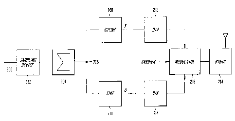
A block diagram of an exemplary system for performing FM modulation
of a signal using digital signal processing is depicted in Figure 2. In the
figure,
an incoming analog signal 200 is sampled and digitized by a sampling device
202. The sampling rate will depend upon various design considerations. In
signals having information conveyed by a phase component of the signal, an
incoming signal 200 can be sampled at a rate of, for example, 80
ksamples/second. A summation device 204 accumulates the digitized samples
generated by the sampling device 202. In accordance with the exemplary DSP
CA 02238332 1998-OS-22
WO 97/19540 PCT/SE96/01486
8
architecture described herein, each sample contains I b-bits of information.
As
part of the phase data extraction process, the samples from the sampling
device
202 are typically upsampled at a higher rate, for example, 240
ksamples/second,
by the summation device 204. As will be appreciated by those skilled in the
art,
upsampling at this rate provides two additional samples for original sample.
The
upsampling process condenses the samples from the sampling device 202 and
facilitates a filtering operation (not shown) used to smooth output generated
by
the summation device 204. For the purpose of illustration, the output from the
summation device 204 is depicted as being provided to a node 20b which sends
the summation device output to cosine and sine component generators 208 and
210. Cosine and sine generators 208 and 210 can, for example, be implemented
as DSP routines which access look-up tables as described below.
Sample information provided by the summation device 204 contains phase
information (described in greater detail below) from which the cosine and sine
component generators, 208 and 210, determine corresponding cosine (1) and sine
(Q} components. The component information is then provided to digital-to-
analog (D/A} converters 2I2 and 2I4, respectively, for conversion of the
component values into corresponding analog signals. The analog signals are
modulated onto a Garner in modulator 216 (e.g., after first being upconverted
to
an intermediate frequency), whose output is provided to a radio processing
part
218 for transmission.
In accordance with the exemplary DSP architecture described herein, the
information generated by the summation device 204 is stored in a 32-bit
register
(not shown. Each 32-bit register sequence represents phase data sampied from
the incoming source signal from which component values can be determined.
However, due to limitations associated with, for example, a particular DSP
architecture used, only a portion of the 32-bit sequence is ordinarily
reliable.
The reliable phase data contained within the 32-bit sequence, or a portion
thereof, is used by the cosine and sine generators, 208 and 210, to address
lookup tables (not shown in Figure 2}. The lookup tables contain sine (Q) and
CA 02238332 1998-OS-22
WO 97/19540 PCT/SE96/OI486
9
cosine (I) quadrature values addressable according to a given phase data value
provided by phase data from the 32-bit sequence.
. Some of the data within the 32-bit sequence (e.g., the least significant
bits
of the phase data sequence) is typically less reliable due to digital signal
processing implications such as architecture constraints, rounding,
truncation,
and cancellation errors. In a given 32-bit sequence provided by the summation
device 204, only 20 to 24 bits of the phase data can typically be relied on.
However, even some of the least significant of these bits (l. e. , bits 21-24)
may
- not be as reliable as the most significant 20 hits. FuII utilization of the
20
i0 reliable bits would correspond to maintaining tables having 2z° or
1,048,576
entries (or IM). Utilization of all of the 20 reliable bits in this manner
would
provide the best available resolution, but at a prohibitive cost in terms of
memory. Another factor to consider with this solution is the DSP architecture
involved. A conventional DSP architecture may not have the bus or register
IS capability to manage 20-bit addresses without cumbersome addressing
schemes.
These schemes can have added costs in the form of additional instruction
cycles
required for their execution. A more practical solution is to disregard a
portion
of the reliable phase data in order to conserve DSP memory and avoid
architecture implications. Even though a portion of the phase data is
disregarded
20 with this solution, a sufficient amount of resolution can still be
maintained, for
most applications, to provide sine and cosine components having an acceptable
error factor.
In accordance with the first embodiment of the present invention, table
sizes are selected to provide a sufficient amount of resolution without
consuming
25 an unacceptable amount of memory. Accordingly, the two main factors
considered in selection of table sizes are resolution requirements and memory
availability. The size of the tables can be selected according to other
factors as
well. These include, but are not limited to: DSP architecture considerations
(e.g., bus and register sizes); the use of on and/or off chip memory for
storage
30 of the tables; the speed of the on- and/or off chip memory in which the
tables are
CA 02238332 1998-05-22
WO 97/19540 PCT/SE96/01486
stored; and processor speed. While 32 bits are provided by the summation ,
device 204, of which 20 bits are generally very reliable, DSP architecture
considerations, such as bus widths, might not render all of these bits readily
available for efficient use in accessing component information. In a DSP
5 architecture having, for example, a 16-bit bus dedicated to the process,
only 16
of the 20 reliable bits may be readily available for efficient component look
up.
Of course, a different DSP architecture may allow for more of the 20 bits of
information to be used or may even provide more than 20 bits of reliable data.
In an exemplary embodiment, resolution may require, for example, 10-
10 bits to provide sufficiently accurate component values. Accordingly, the 10
most
reliable bits of the readily available 16 bits of phase data are used to
access
tables having 21°, or 1024 entries each. Two '1024 entry tables, one
for cosine
components and ane for sine components, are stored in memory. Hence, for
each quadrature component, there are 1024 increments spanning the possible
values (e.g., 1024 incremental values between -~r and ~r). Figure 3(a)
pictorially
illustrates canine and sine tables 302 and 304 in accordance with this
exemplary
embodiment of the invention. It will be appreciated that the sine component
information in the table in Figure 3(a) can be addressed by adding 1024 to a
cosine table entry address. In the exemplary embodiment described, the lookup
tables are accessed using the 10 most reliable bits of phase data available
from
32-bit sequence provided by the summation device 204. In view of the 10-bit
resolution of the exemplary embodiment, the six least significant bits of the
16-
bits of available phase data are stripped off by a DSP routine. Any additional
phase information (reliable or otherwise) in the 32-bit samples is ignored.
It is readily apparent that greater resolution in the first embodiment
requires use of a greater amount of phase data in the 32-bit sequence provided
by
summation device 204. For instance, if 14-bit resolution were desired, the I4
most reliable bits of the phase data could be used to access at least one
table
having 2I4 or 16,384 entries. This would provide better resolution than using
only 10 bits, however, at the expense of processor memory.
CA 02238332 1998-OS-22
WO 97/19540 PCT/SE96/01486
11
The embodiment described above discloses individual sine
and cosine
tables. Individual tables are provided to allow for the introduction
calibration
factors to compensate for gain and offset variations associated
with analog
components in radio sets. Hence, the component values in
each table might be
adjusted individually to compensate for these gain variations.
In the event that a radio set is manually calibrated (i.e.,
using adjustable
components such as potentiometers, etc.) at the factory,
or at an installation
point, to adjust for variations, such variations need not
be compensated for in the
sine and cosine tables. In this situation, a single table
can be used. Hence, in a
manually adjusted radio set having, for example, a single
cosine component
table, a corresponding sine component value can simply be
derived by
subtracting 90 or ~r/2 from the cosine component value derived
from the table.
In accordance with a second exemplary embodiment of the present
invention, component values are derived using phase data
that is separated into
two parts. A first part is used to access one or more tables
containing
component information. A second part is used to calculate
an offset value that is
added to a component value derived from a table using the
first part. The tables
contain cosine and sine base component information and difference
information
that corresponds to differences between consecutive base
component values. The
difference information is used in conjunction with the second
part of the phase
data to calculate the offset value. The offset value is added
to a base value to
produce a component value for output. In this second exemplary
embodiment of
the invention, less memory is used, albeit at the expense
of one or more
instruction cycles that are used to calculate and add the
offset value. However,
some speed can be recovered because smaller tables are used
which can be stored
' in high-speed memory.
Figure 3(b) illustrates an exemplary memory configuration
for sine and
cosine tables according to the second embodiment of the invention,
the usage of
which by cosine 208 and sine 210 generators will now be described
below. Note
CA 02238332 1998-OS-22
WO 97119540 PCT/SE96/OI486
12
that for the second exemplary embodiment described, the tables of Figure 3(a)
are four times the size of the tables of Figure 3(b).
In an exemplary arrangement in accordance with the second embodiment
of the invention, I6-bits of the available phase data from a 32-bit sequence
(generated by the summation device 204) are used. The 16-bits are arranged in
a
two-part format wherein a first sequence of 7-bits is used to address the four
tables 306, 308, 310 and 312. Accordingly, each table contains 2', or 128
entries. A first table 306 and a second table 312 contain sine (Q) and cosine
(I)
base values, respectively. The third table 308 and a fourth table 310 contain
the
values of differences between consecutive base values in the first and second
tables, respectively. To determine a Q component, the first part of the two-
part
phase data is used to address the sine 306 and sine' 308 tables. Similarly, to
determine an I component, the first part of the phase data is used to address
the
cosine 312 and cosine' 310 tables.
A second part of the phase information, in accordance with the second
exemplary embodiment, consists of a sequence of 9-bits (of the 16-bits of
available phase data} which represent an offset factor. The offset factor is
used
in conjunction with a corresponding difference value (derived from a
difference
value table 308 and 310) to calculate an offset value. The offset value is
then
added to a (cosine or sine) base value (from tables 306 and 312) to determine
the
component value that is provided to a D/A converter. A component value (I or
Q) is calculated in accordance with Equation 1:
CA 02238332 1998-OS-22
WO 97!19540 PCT/SE96/01486
13
component = A + offset*(B A) (1)
wherein:
:.
A is a base component value retrieved from a cosine or sine
base component value table;
(B A) is a difference between consecutive base values, A and B,
retrieved from a cosine or sine difference value table; and
offset is the offset factor from the second part of the phase data.
An example of determining a Q {sine) component, in accordance with the
second embodiment of the invention set out above, is described with respect to
the flow diagram depicted in Figure 4. Phase data {in the form of a 16-bit
sequence) contained in a 32-bit sequence produced by summation device 204 is
derived at block 400. With respect to determining a sine component value, a
first 7-bit part of the 16-bit sequence is used to address table 306 to
retrieve a
sine base component value (block 402). The first 7-bit part is further used to
address table 308 to retrieve a difference value which is a difference between
the
sine base value retrieved at block 402 and a next consecutive sine base value
in
the first table (block 404). Accessing the corresponding difference value may
be
performed, for example, by adding 128 to an address pointer of the address
used
to access the sine base value table 306. Of course, the cosine difference
component value can be accessed from table 310 by adding an additional 128 to
the address pointer.
The difference value derived from table 308 is used in conjunction with
an offset factor provided by the second 9-bit part (of the 16-bit sequence) to
' produce an offset value. In a preferred embodiment, calculation of the
offset
value is performed (at block 406) by multiplying the offset factor with the
sine
difference value retrieved from table 308. The offset value is then added to
the
sine base value retrieved at block 402 to determine the sine (Q) component
(block 408) that is provided for output {block 410). A similar procedure can
be
CA 02238332 1998-OS-22
WO 97!19540 PCT/SE96/01486
I4
performed to determine the cosine component values, albeit using the
apgropriate
cosine tables 310 and 312.
The four tables 306, 308, 310 and 312, arranged in accordance with this
exemplary embodiment of the invention, each contain 128 entries. However,
those skilled in the art will readily appreciate that table size is
discretionary
depending on particular performance requirements and system capabilities. In
accordance with a preferred embodiment, the tables are organized in a
consecutive memory address arrangement in a DSP memory. The sine base
value table 306 is followed by the sine difference value table (sine') 308,
which
sine difference values are followed by cosine difference values (cosine') 3I0,
which cosine difference values 410 are followed by cosine base values 312.
Arranging the tables in this way takes advantage of the particular DSP
architecture characteristics associated with the exemplary embodiments
described
herein. In particular, this arrangement of the tables described takes
advantage of
IS DSP architecture characteristics of the Texas Instruments TMS320c5x family
of
processors, which processors can be used in practicing the invention. However,
the particular arrangement described is discretionary, and other processor
architectures may call for different table arrangements to achieve a desired
result.
Some advantages of utilizing arrangements, or operating with methods in
accordance with the invention are illustrated in Figures 5(a) and 5(b). The
-. graphs provided in these figures are not to scale. Because the number of
incrementations for the entire range of phase component values is limited by
the
amount of DSP memory reasonably available, an actual phase value may fall
between consecutive incremental values stored in a conventional sine or cosine
look-up table. Figure 5(a) is a graph depicting generation of a component
value
using a system in accordance with the first embodiment of the invention ,
described above. In the graph, points C and D on the phase (horizontal) axis
represent incremental phase values corresponding to a 10-bit phase sequence .
from the 32-bit sequence. The actual phase value is shown at point X.
Corresponding table values for points C and D from the 1024-entry table of
CA 02238332 1998-OS-22
WO 97/19540 PCT/SE96/01486
Figure 3(a) are shown on the vertical axis at positions C' and D'. The
corresponding phase component value for the actual value (not stored in the
table
of Figure 3(a)) is shown at X'. In operation, the conventional arrangement
produces the value corresponding to C' when the phase value X is received by a
5 cosine (i) or sine (~ component generator. Consequently, an error amount,
which is the difference between the values of C' and X', exists. This error
amount is reduced by providing higher resolution. Higher resolution usually
involves using a larger amount of phase data to access correspondingly larger
tables.
10 Figure 5(b) is a graph depicting generation of a component value in an
arrangement incorporating the second exemplary embodiment of the invention
described above. In the graph, points A and B on the horizontal axis represent
possible phase values from the first 7-bit sequence of the 16-bit phase data .
sequence. The actual phase value is shown at point X. It is readily apparent
that
15 the system incorporating the first embodiment provides approximately eight
stored incremental values for every one base value increment stored according
to
the second embodiment (i.e., 2'° versus 2'). Corresponding table values
for A
and B, retrieved from one of the 128-entry base value tables 30b and 312, are
shown on the vertical axis at points A' and B' . The actual corresponding
phase
component value is shown at X' . In operation, the arrangement produces a
component value in accordance with Equation 1. That is, an offset value
calculated by multiplying an offset factor with the difference between A' and
B'
(which difference is retrieved from a difference value table) is added to the
base
value corresponding to A' {retrieved from a base value table). The offset
value
can be illustrated by a line 500 in Figure 5{b). The line 500 corresponds to
' possible offset values. The line 500 is comprised of a number of data points
corresponding to the offset value. Hence, for the exemplary 9-bit offset
factor
described above, the line 500 consists of 29 or 512 possible offset values. It
should be noted that Figure 5(b) (and Figure 5(a)) is not to scale and only
provided to illustrate operation in accordance with the exemplary embodiments
CA 02238332 1998-OS-22
WO 97/19540 H'CT/SE96/01486
I6
described herein. For instance, the line 500 ordinarily conforms very closely
to
the phase curve between consecutive base component values. By adding the
offset value to the base component value A', the component value produced can
,
be nearer to the actual value of X' than the value provided by systems
according
to the first embodiment (e.g., C' in Figure 5(a)). This can be readily
appreciated by considering the case where A' and C' happen to be the same
value. In such a case, the system incorporating the first embodiment produces
a
component value of C', while a system incorporating the second exemplary
embodiment of the invention produces a component value corresponding to A'
plus an offset value.
Apparatuses and methods incorporating the invention utilize readily
available phase data produced by a sampling arrangement. It will be
appreciated
by one skilled in the art that determining a phase component using a greater
number of bits of information generally provides greater resolution. In the
second described exemplary embodiment, a greater amount of phase information
is used to derive I and Q components by breaking up the available phase
information. Additional information used in the second exemplary embodiment
might otherwise be disregarded in the first exemplary embodiment (because of
memory constraints). The cost of the additional resolution provided by the
second exemplary embodiment is in additional instructions cycles required for
offset value calculation and addition. However, systems operating in
accordance
with the second exemplary embodiment can use smaller tables, thereby
conserving memory. Because the tables can be relatively small, they can be
stored in high-speed memory (e.g., SRAM) which provides time savings
compared to the memory types typically used to store the {larger) tables
associated with the first exemplary embodiment. '
The expense of possible additional table access and additional calculation
involved in systems incorporating the second exemplary embodiment also is
offset by the increased accuracy provided for a given amount of memory used.
This enhanced accuracy reduces the amount of component error. For example,
CA 02238332 1998-OS-22
WO 97/19540 PCT/SE96/01486
17
in systems according to the first exemplary embodiment described above (i.e.,
10-bit resolution), table derived component values were found to have a
maximum phase component deviation, that is difference from an actual phase
component value (e.g., C' versus X'), in the vicinity of 0.3%. In systems
operating in accordance with the second exemplary embodiment of the invention
(i.e., 7-bit table address, 9-bit offset factor), a maximum error was found to
be
approximately 0.04 % .
The advantages provided by systems incorporating the invention can be
illustrated by comparing the output transmission waveforms illustrated in
Figures
6(a) and 6(b). Figure 6(a) depicts a relative power spectrum of a filtered
modulated carrier signal in accordance with the exemplary arrangement
described
for the first embodiment of the invention, while Figure 6(b) depicts a
relative
power spectrum of the same modulated carrier signal in a system in accordance
with the described exemplary arrangement in accordance with the second
exemplary embodiment. By comparing these graphs, it is readily apparent that
signal power in the sideband portions (i.e., ~ 30 kHz) of the spectrum is
diminished in the scenario depicting utilization of the system incorporating
the
exemplary second embodiment of the invention. Reduced power emission in the
sideband is desirable to reduce, among other things, adjacent channel
interference. This interference is due, in part, to phase deviation (errors)
in the
-- values provided by the cosine and sine (I and Q) component generators 208
and
210. Of course, reduced sideband power emissions can be achieved in systems
according to the first exemplary embodiment by increasing signal resolution.
The invention has been described with reference to particular exemplary
embodiments. However, it will he readily apparent to those skilled in the art
that it is possible to embody the invention in specific forms other than those
of
the preferred embodiments described above. Exemplary utilization of the
invention described herein discloses application in a particular DSP
architecture.
However, it also is possible to embody the invention in a programmed
application earned out by use of a general purpose processor, an ASIC, or by
CA 02238332 1998-OS-22
WO 97/19540 PCT/SE96/01486
18
discrete processing components. Embodiment of the invention in such a way
may be done without departing from the spirit of the invention. .
The table arrangements also have been described with reference to
particular exemplary embodiments. However, it will be readily apparent to
those '
skilled in the art that it is possible to organize and store one or more
tables in a
variety of ways. For example, in the second embodiment, a single component
table can be used whose entries contain both base and difference values.
Moreover, the two-part phase data format can be organized in a variety of ways
to achieve a desired result. For example, if processor architecture
characteristics
permit, a greater number of phase data bits can be dedicated to the table
address
or to the offset factor. The 32-bit phase data sequence provided by a Texas
Instruments TMS320c5x DSP can readily provide 20-bits of reliable phase data.
Therefore, an alternate two-part phase data arrangement may comprise a 7-bit
address and a 13-bit offset factor. In addition, an input signal 200 may
already
be in a digital format whereby phase data can be derived directly for purposes
of
accessing one, or more component tables, or for calculation of an offset
value.
Therefore, the embodiments described herein are merely illustrative and
should not be considered restrictive in any way. The scope of the invention is
given by the appended claims, rather than by the preceding description, and
all
variations and equivalents which fall within the range of the claims are
intended
_- to be embraced therein.