Note: Descriptions are shown in the official language in which they were submitted.
CA 02239087 1998-OS-28
VIDEO IMAGING DEVICE
Background Information
The invention relates to a video im~ging device according to the definition of the species
in Claim 1.
Video im:~ging devices having at least one photodetector per picture element to be
recorded have become known as so-called CCD cameras, where a lens is arranged infront of a semiconductor sensor cont~ining the photodetectors in a raster shape.
A device is known from German DE-A-3 1 40 217 for reading a master surface having
image information, whereby the device moves the image information using a
photosensor for im~ging via a plurality of im~ging systems. The known device has,
however, a fixed object width, and the im~ging systems are not able to change the
viewing angle of the reading device.
Therefore, the object of the invention is to devise a video im~ging device which will
elimin~te these disadvantages.
The video im~ging device according to the present invention is able to record images of
objects disposed oppositely to it with substantial depth of focus. If the individual
photodetectors are spaced apart at the same distances (grid dimensions) as the focusing
elements, then images are always formed on a scale of I to 1.
An advantageous method for manufacturing the video im~ging device of present
invention is rendered possible in a further refinement by constituting the focusing
element as a refractive microlens, a refractive Fresnel microlens or a stepped plate, the
focusing elements for all picture elements to be imaged being formed by structurally
defining a transparent carrier base.
Provision is made in another refinement for a plurality of optionally actuatablephotodetectors to be assigned in each instance to one focusing element. With the aid of a
device having one or a few lines of focusing elements, this further refinement enables a
CA 02239087 1998-0~-28
planar image to be recorded by sc~nnin~ transversely to the line orientation. However,
this further refinement also makes it possible, when working with an already planar, i.e.,
raster-type arrangement of the photodetectors and of the focusing elements, to
electrically alter the viewing direction of the video im~oing device.
One advantageous embodiment of the video im~ging device according to the presentinvention provides for the structures of the focusing elements to be rotationally
symmetric, the optical midpoint being disposed in the middle of the surface assigned, as
the case may be, to a focusing element. This embodiment is intended, first and foremost,
for recording objects situated right in front of the video im~ging device. In this context,
the further refinement mentioned above makes it possible to rotate the viewing direction.
Another advantagéous embodiment is conceived for a viewing direction that deviates
therefrom, in that the focusing element has an asymmetrical construction, so that an
oblique viewing direction results in response to a centrically arranged photodetector.
When working with the video im~ging device according to the present invention, an
image of the object parts that are not to be picked up by a photodetector is formed next to
the photodetector. To ensure that the quality is not degraded by scattered light, another
embodiment of the invention provides that the surfaces of a carrier base bearing the
photodetector, the surfaces not being covered with photodetectors, be developed as
absorbing surfaces.
One embodiment of the video im~ging device according to the present invention for
picking up colored images is rendered possible in that color filters of different colors are
assigned to the photodetectors.
As is the case when working with other video im~gin~ devices, the light impinging upon
the photodetector can be converted into an electric signal by generating a charge
corresponding to the quantity of light. Since the quantity of light for each photodetector
in the case of the video im~ging device according to the present invention is very small,
it is preferably proposed to provide for single electron-tunnel components to read out the
CA 02239087 1998-0~-28
charge produced in each instance in a photodetector as a function of the light intensity.
Single electron-tunnel components (SED = single electron devices) are described, for
example, in A. H. Clealand, "The Detection and Manipulation of Single Electrons",
Digest of Papers MicroProcess '94, 7th International MicroProcess Conference, Hsinchu,
Taiwan, July 11-14, 1994, pp. 146-149.
Due to their size, however, the described components must be operated as cooled
components to achieve a sufficient signal-to-interference ratio. The need for this is
elimin:~tc.l however, in a further refinement of the invention, where the structures of the
single electron-tunnel components are smaller than 10 nm. In this context, printed circuit
traces are preferably applied lithographically to the carrier bases bearing the
photodetectors for supplying voltage and for diverting the signals.
A number of applications, such as video telephones, require simultaneously recording an
image to be sought and reproducing a received image. This can be achieved quite
advantageously with the video im~ging device according to the present invention by
using a video screen, in particular a color video screen, designed for a dual function.
In one advantageous refinement of a recording and reproducing device of this kind,
provision is made for a hollow space to be arranged between the carrier base forming the
focusing element and the carrier base for the photodetectors, for luminescent surface
elements to be applied to the inner side of the carrier base for the focusing elements, and
for controllable electron sources to be configured on the carrier base for the
photodetectors, each of the electron sources being assigned to a luminescent surface
element.
Another advantageous refinement of a recording and reproducing device proposes that an
additional carrier base for luminescent surface elements of the video screen rest on the
carrier base for the focusing elements, and that an additional carrier base for the
controllable electron sources be provided parallel to the carrier base for the
photodetectors .
CA 02239087 1998-0~-28
In these embodiments, it is preferable that the controllable electron sources beconstituted, as the case may be, by at least one emitter tip and by extractor wires.
The emitter tips and extractor wires are preferably produced by means of corpuscular
S beam-induced deposition. The Patent Application P 44 16 597.8 ofthe applicant
describes the manufacture of these picture-element radiation sources.
To prevent the photodetectors from being illllmin~ted by the luminescent surfaceelements, provision can be made according to another embodiment of the invention for
the electron sources and the photodetectors to be operated in time-division multiplexing
mode.
Exemplary embodiments of the invention are illustrated in the drawing on the basis of
several Figures and elucidated in the following description. The Figures show:
Figure 1 a section through a part of a first exemplary embodiment having a
mlcrolens;
Figure 2 a section through a part of a second exemplary embodiment having a
microlens;
Figure 3 a section through a first exemplary embodiment having a Fresnel
~ microlens;
Figure 4 a section through a second exemplary embodiment having a Fresnel
microlens;
Figure 5 an application example of an image- reproducing and image-recording
device according to the present invention;
Figure 6 an enlarged schematic representation of an exemplary embodiment of a
CA 02239087 1998-0~-28
photodetector;
Figure 7 a section through a first exemplary embodiment of an image-reproducing
and image-recording device; and
Figure 8 a section through a second exemplary embodiment of an image-
reproducing and image-recording device.
In the video imaging device depicted in Figure 1, microlenses 2 are arranged in a raster
form, with a grid element spacing d on a first carrier base 1. Situated in the focal plane
of the microlenses, on a second carrier base 3, in each case opposite a microlens, are
photodetectors 4, whose dimensions are set to be small, to the extent that their images on
the object to be recorded (not shown) still correspond, even given the largest object width
provided by the video im~ging device according to the present invention, to about the
size of the microlenses. Microlenses 2 are configured in a compact side-by-side
arrangement, so that one microlens forms the image of one picture element of the object
on a photodetector 4. The interstitial spaces between photodetectors 4 can be
unassigned. Preferably, a blackening prevents a diffused reflection of the lightimpinging from adjacent picture elements of the object, which in turn would lead to
scattered light. The arrangement can include other photodetectors 5, 6 as well, however.
For example, if photodetector 5 is used in place of photodetector 4, then the video
im:~ging device "looks" to the side in accordance with dot-dash line 7. This can follow in
a statical operation - i.e., a lasting or continuing angle can be adjusted - or in an operation
that changes in rapid succession, so that an image-scanning motion results.
In the exemplary embodiment according to Figure 2, microlens 2 is mounted on a prism
8, so that the video im~ging device already "looks" to the side with an angle ~, when
photodetector 4 is disposed opposite the middle of microlens 2. In addition, the viewing
angle can be changed by selecting one of photodetectors 4, 5, 6.
In the exemplary embodiments according to Figures 3 and 4, a Fresnel microlens is
CA 02239087 1998-0~-28
provided in each case as a focusing element. In comparison to Fresnel microlens 10
shown in Figure 3, Fresnel microlens 11 in the e~emplary embodiment according toFigure 4 has an asymmetrical form, so that the camera "looks to the side" with respect to
a centrically arranged photodetector 4.
s
Figure 5 depicts an application example of a video-recording and -reproducing device
according to the present invention, which is used as a flat video screen 11 on a desk 12.
A person 13 using the device according to the present invention can look at the video
screen. In addition, an image of the head of person 13 can be recorded and transmitted,
since he or she is situated in recording area 14. Objects within recording area 14 are
recorded with a constant im~ging scale. When using the video im~ging device of the
present invention, there is no need to focus to a specific object width. A sharp image of
the object is formed, for as long as it is situated in recording area 14.
In the illustration in Figure 5, the camera "looks" at an angle that deviates from 90~.
When the video im~ging device according to the present invention is designed
accordingly, this angle can be electronically adjusted and, thus, adapted to the particular
circumstances.
Figure 6 schematically depicts a photodetector, which essentially includes two
conductive electrodes 15, 16, which are arranged in a vacuum 17. When a color-
recording device is used, layer 18 covering the photodetector is constituted as a color
filter. Electrode 15 is transparent and receives an accelerating voltage U, which amounts
to a few 100 V. Arriving photons 20 penetrate electrode 15 and impinge upon electrode
16, which is designed, e.g., is provided with an alkali metal coating, to emit
photoelectrons. The emerging electrons are pulled toward electrode 15 by the
accelerating voltage. The voltage changes produced by the emerging electrons aresuitably amplified in an amplifier 20 arranged on same carrier base 19. Printed circuit
traces and circuit arrangements (not shown) effect in a generally known way a sequential
sampling of the output signals from the photodetectors, so that a video signal is formed.
CA 02239087 1998-0~-28
Suitable as amplifiers are, preferably, so-called single-electron amplifiers. Optionally,
three photodetectors assigned to one basic color each can be sequentially connected to an
amplifier.
Figures 7 and 8 each show schematic details of a video recording and video reproducing
device, the exemplary embodiment according to Figure 7 using in each case the same
carrier bases for the components of the video reproducing device as for the video
recording device and, for that, separate carrier bases being provided in the exemplary
embodiment according to Figure 8.
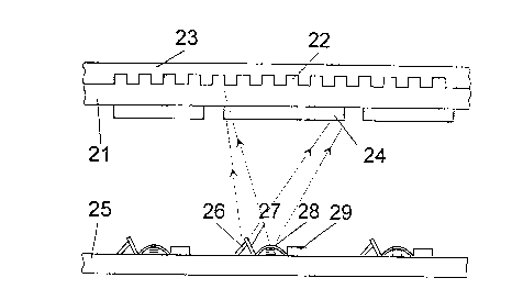
Transparent carrier base 21 in the exemplary embodiment according to Figure 7 isstructurally formed on its top side with stepped plates 22 arranged in a raster shape, each
having an edge length of 300 ~lm. In addition, transparent carrier base 21 is provided
with a protective layer 23. Disposed on the inner side of carrier base 21 is - likewise in a
transparent construction - per stepped plate, a surface element 24 of the video screen.
Suited as luminescent material for the video screen or for its surface elements are, for
example, indium tin oxide or tin oxide.
At a predefined distance thereto - for example 300 !lm - is disposed carrier base 25 for
the electron emitters and the photodetectors. Both are shown, substantially enlarged, in
comparison to the distance between carrier bases 21, 25 and in comparison to stepped
plate 22 and surface element 24. Thus, for example, the width of a photodetector,
inclusive of the amplifier, is about 20 ~lm, while about 3 ~Im are provided for an electron
emitter.
A suitable electron emitter is described in detail in the Patent Application P 44 16 597.8
of the applicant, inclusive of a manufacturing method with the aid of additive electron or
ion-beam lithography, usmg corpuscular beam-induced deposition. Therefore, further
clarification is not needed for an understanding of the invention. An electron emitter
includes, in each case, at least one emitter wire 26 and at least one extractor wire 27,
which is linked to a somewhat higher potential than emitter wire 26. The emerging
CA 02239087 1998-0~-28
electrons are accelerated toward surface element 24 of the video screen. The brightness
is able to be controlled both via the potential of extractor wires 27 as well as via the
voltage being applied to surface element 24 of the video screen.
Besides the electron emitters, photodetectors 28 and amplifiers 29, as were described, for
example, in connection with Figure 6, are arranged on carrier base 25. The light from the
picture element in question of the object to be imaged impinging upon stepped plate 22 is
focused at photodetector 28.
Due to the movement of electrons from the electron emitters to the video screen, a
vacuum is required between carrier bases 21 and 25. To m~int~in a spacing, i.e., to resist
the pressure produced by the vacuum, as is generally known, glass pearls can be inserted
between carrier bases 21, 25 at positions not needed for video im~ging and reproduction.
In the exemplary embodiment according to Figure 8, besides a carrier base 31, which
forms the stepped plates, provision is made for a carrier base 32 for surface elements 24
of the video screen and, besides carrier base 33 for photodetectors 28, provision is made
for a carrier base 34 for electron emitters 26, 27. Between carrier base 33 and carrier
base 34 is a protective layer 30.