Note: Descriptions are shown in the official language in which they were submitted.
CA 02239S81 1998-06-26
DEVICE FOR THE GENERATION OF ANALOG SIGNALS
THROUGH DIGITAL-ANALOG CONVERTERS,
ESPECIALLY FOR DIRECT DIGITAL SYNTHESIS
BACKGROUND OF THE INVENTION
1. Field ofthe Invention
The present invention relates to a device for the generation of
analog signals by means of analog-digital converters. It can be applied
especially to the field of the direct digital synthesis. More generally, it can be
applied to the generation of analog signals starting from digital-analog
0 converters where, for example, it is necessary to reduce the effect of non-
linearity of these converters.
2. Description of the Prior Art
Direct digital synthesis is a technique of frequency synthesis
wherein the samples of the sinusoidal signal to be generated are prepared in
digital mode and these samples are converted into analog form by means of
a digital-analog converter, hereinafter called a DAC. The frequency
synthesizers obtained by this technique are highly attractive in terms of
volume, weight and energy consumption for they can benefit from large-scale
integration. Their other advantages are in particular very high resolution and
20 very small switching times.
One drawback of direct digital synthesizers according to the prior
art is that the spectrum of the output signal shows many parasitic lines.
Indeed, at the input of the DAC of the synthesizer, the amplitude of the
signal is encoded on a number of bits M which is generally smaller than the
25 number of bits N of the digital signal prepared. The passage from N bits to
M bits generates an error of quantification or truncation that results in the
presence of parasitic lines on the output signal.
In addition, because of the above-mentioned quantification, the
transfer function of the DAC, i.e. the output voltage as a function of the input30 digital words, is a stepped function. These non-linearities then designate the
fact then that the steps are not of equal heights. These non-linearities are
added to the above mentioned errors of quantification, and are thus defects
of the transfer function as compared with an ideal transfer function where the
CA 02239~8l l998-06-26
steps would have the same height. The non-linearities of the DAC result in
the generation of harmonic frequencies which are aliased owing to the
sampling. In other words, parasitic lines are thus created, a parasitic line
being a spectral component located at frequencies different from that of the
5 fundamental component of the signal to be synthesized.
According to a known method for eliminating the amplitude
quantification and reducing the non-linearities of a DAC, a high amplitude
random noise is added to the prepared digital signal, present at the input of
the DAC. This random noise is then removed in an analog manner by a
second DAC. This method is described for example in the European patent
application EP 0452031. The disadvantage of this method is that it lowers
the performance characteristics of the phase noise of a direct digital
synthesizer especially because of the injection of noise and the difficulty in
matching the two DACs.
SUMMARY OF THE INVENTION
The goal of the invention in particular is to improve the spectral
purity of direct digital synthesizers by reducing the level of the parasitic lines,
in doing so without lowering the noise performance characteristics. To this
end, an object of the invention is an analog signal generation device
20 comprising a block for the generation of words encoded on N bits and an
analog-digital converter whose input is encoded on M bits, M being smaller
than N, the device furthermore comprising a sigma-delta modulator, at the
output of the first block, the bus being separated into M most significant bits
reserved for the input of the analog-digital converter and N-M least significantbits that enter the sigma-delta modulator, the output of this modulator being
an M-bit bus that is added to the M output bits of the word generation block
by digital addition means, the result of the addition constituting the input
signal of the analog-digital converter.
The main advantages of the invention are that it minimizes the
increase in the basic level of the phase noise of a digital synthesizer, can be
adapted to all kinds of systems for the generation of analog signals from
~ CA 02239~81 1998-06-26
analog-digital converters and is compact, simple to implement and
economical.
BRIEF DESCRIPTION OF THE DRAWINGS
Other features and advantages of the invention shall appear from
5 the following description made with reference to the appended drawings of
which:
- Figure 1 is a block diagram of an exemplary embodiment of a
prior art device;
- Figure 2 is a block diagram of an exemplary embodiment of a
10 device according to the invention;
- Figures 3 to 6 provide an illustration in the frequency domain of
the role of a sigma-delta modulator in a device according to the invention;
- Figure 7 is a block diagram of an exemplary sigma-delta
implanted in a device according to the invention.
MORE DETAILED DESCRIPTION
The invention is described with reference to direct digital
synthesizers. However, it can be applied to other types of devices for the
generation of signals from digital data.
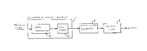
Figure 1 is a block diagram of a direct digital synthesizer
according to the prior art. This synthesizer comprises for example three
main blocks 1, 2, 3. A block 1 for the generation of digital samples of the
sinusoidal signal to be synthesized receives a digital word for frequency
control and a clock signal. Conventionally, this block 1 comprises a phase
accumulator 11 and a memory 12 containing the sine function. The phase
accumulator 11 comprises for example a digitized ramp generator connected
to the address bus of the memory 12 containing the sine function. The
output of this first block 1 is connected to the input of a block 2 for the
conversion of the digital samples delivered by this first block 1 into an analogsignal. The DAC is contained in this block 2 or constitutes it. The output of
30 this second block 2 is connected to the input of a low-pass filtering block 3which makes it possible for example to eliminate the spectral components
related to the sampling. This third block 3 delivers the output analog signal
CA 02239~81 1998-06-26
of the synthesizer. As indicated previously, a major disadvantage of this
direct digital synthesizer is that the spectrum of the output signal has many
parasitic lines. They are due in particular to two main causes pertaining to
the process of digital-analog conversion described previously. A first cause
5 is the quantification of the amplitude and a second cause is the non-linearity of the DAC used.
Figure 2 is a block diagram of an exemplary embodiment of a
direct digital synthesizer according to the invention. A sigma-delta modulator
21 is interposed between the block 1 for the generation of the digital samples
or for the generation of the words to be converted, and the digital-analog
conversion block 2. There is a known way of using a modulator of this kind
to pass from an N-bit word to an M-bit word, M being smaller than N, by
eliminating the truncation error in the useful signal band, which is the band inwhich the sine signal or another signal is synthesized. The spectral
components related to this truncation are then rejected from this band.
According to the invention, a high-order sigma-delta modulator is used not
only to cancel the quantification error but also to greatly reduce the effects of
non-linearity of the DAC. Thus, according to the invention, the sigma-delta
modulator is used above all to solve the problem of non-linearity, and
advantageously it also eliminates the truncation errors.
At the output of the first block 1, the bus is separated into M most
significant bits that enter for example a delay module 22, and N-M least
significant bits that enter the sigma-delta modulator 21. The output of this
modulator is an M-bit added to the M output bits of the delay module 22 by
digital addition means 23. The delay created by the delay module 22
corresponds to the time taken by the sigma-delta modulator to process a
word between its input and its output. The result of the addition constitutes
the input signal of the digital-analog converter 2. The low-pass filter 3
connected for example to the output of this digital-analog converter 2
eliminates the spectral components related to the sampling as well as those
generated by the sigma-delta modulator 21. The input signal of this
modulator 21 is the error ~ made by truncating the word from N bits to M bits.
~ CA 02239~8l l998-06-26
A clock 24 provides for example a clock signal with a frequency Fo common
to the modulator 21, the analog-digital converter 2 and the delay module 22.
Figures 3 to 6 which follow illustrate the role of the sigma-delta modulator.
They represent the amplitudes of the lines of the digital signals concerned as
5 a function of the frequency F. With regard to the sigma-delta modulator, the
number of bits M at output of the modulator is not related to the number of
truncated bits N-M. This especially results from the fact that the invention
uses only sigma-delta modulators that generate overflows. It is in particular
this overflow mechanism that makes it possible to resolve the problem of the
10 non-linearity of the digital-analog converter.
Figure 3 illustrates the spectrum of the signal at a point A located
at the input of the delay module 22. More specifically, it represents the
amplitude Am of the spectral components of the signal as a function of the
frequency F in an interval ranging between the null frequency o and the clock
frequency Fo. This signal includes the M most significant bits of the word to
be converted. It comprises for example two useful lines 31, 32
corresponding to the signal to be synthesized. In fact, one line 31 is the
useful line and the other line 32 is the useful line that is aliased because of
the sampling. These lines are symmetrical with respect to half of the clock
20 frequency Fo. Parasitic lines 33, 34 correspond to the truncation of the digital
signal or word to be converted, this truncation corresponding to the N-M least
significant bits of the signal.
Figure 4 illustrates the spectrum of the signal at a point B located
at the input of the sigma-delta modulator 21. This signal comprises the N-M
least significant bits of the word to be converted. The lines 41, 42 of this
signal have the same amplitudes as the parasitic lines 33, 34 of the signal at
the input A of the delay module 22. They are opposite and are located at the
same frequencies.
Figure ~ illustrates the spectrum of the signal at a point C located
at output of the sigma-delta modulator 21. The output of this modulator is for
example prepared so that it comprises the same number of bits as the signal
at the input A of the delay module 22 and so that its expression is the sum of
CA 02239~8l l998-06-26
the above mentioned error ~ with a digital signal decorrelated from the signal
to be synthesize or generated, i.e. in fact decorrelated from the truncated
word, represented by the useful lines 31, 32 in figure 3. To the lines 41, 42
of the error signal ~ there are therefore added lines 51 decorrelated from the
5 useful signal and this error signal ~. The term 'decorrelated' means in
particular that no correlation function exists between the signals.
Figure 6 illustrates the spectrum of the signal at a point D located
at the input of the digital-analog converter, therefore after the addition of the
signals coming from the delay module 22 and the sigma-delta modulator.
The lines 41, 42 of the error signal ~ get cancelled out with the parasitic lines
33, 34 of the signal at the input A of the delay module 22. The lines 51 of
the decorrelated signal remain in the presence of the useful lines 31, 32.
The signal 51 is located in the spectral field outside the band where the
useful signals 31, 32 are synthesized, making it possible to eliminate this
signal 51 by a filtering operation after the digital-analog conversion, for
example by the low-pass filter 3 at output of the digital-analog converter 2.
Preferably, the amplitude of the decorrelated signal 51 is close to
that of the useful signal to be synthesized. It may even be higher than that of
the useful signal. Thus, for a given value of the output word of the digital
sample generation block 1, the signal at input of the digital-analog converter
2 takes up a major part of the operating range of this converter 2. This
makes it possible to smoothen its defects of non-linearity and hence
significantly reduce the parasitic lines due to these defects, in doing so by
eliminating the quantification noise corresponding to the truncation of the
signal from N to M bits. The problem of the amplitude quantification and the
problem of the non-linearity of the digital-analog converter are thus resolved
concomitantly by the device according to the invention, without any
introduction of noise.
Indeed, in a preferred embodiment, the output signal of the
modulator 21 is expressed by means of an equation on the Z-transforms, the
CA 02239~8l l998-06-26
Z-transform of the signal S(z) being given for example by the following
relationship:
S(z) = z ~(z)- Q(1-z )~ (1)
z~~ represents a delay that is compensated for by the delay
5 module 22, ~ designates the order of the sigma-delta modulator 21.
Preferably this order is high, for example equal to M-1, where M is the
number of bits of the analog-digital converter 2. A high-order modulator in
particular makes it possible to linearize the analog-digital converter by
delivering a signal whose energy sweeps through at least half of the range of
this converter. ~(Z) represents the z transform of the error signal.
The term Q(1-z~ represents the above-mentioned decorrelated
signal 51. This signal for example is located in the spectral domain around
the frequency Fo /2 where Fo is the frequency of the clock signal 24. It is
thus located at a place of the spectrum where the synthesis of a signal with a
frequency Fx is generally of no utility because of the difficulty of filtering the
frequency aliased by sampling which is equal to Fo - Fx
Figure 7 uses a block diagram to illustrate an exemplary sigma-
delta modulator 21 that can be implanted in a device according to the
invention. With the overflow mechanism, the least significant bit of the
20 output bus of the sigma-delta modulator 21 has the same place value as the
least significant bit of the M-bit bus obtained after truncation. The addition of
the output of the modulator 21 with the M-bit bus must be done in obtaining a
correspondence between the least significant bits. This is the only constraint.
Thus, if the bus at output of the modulator is an M-bit bus, the addition with
the M-bit bus, resulting from the truncation of the N-bit word, gives at most
one M+1 bit bus. In fact, the result of the addition 23 may be an M-bit bus in
taking account, in the initial N-bit bus, of the fact that there will be an
addition, the amplitudes being managed in the N-bit bus so that the addition
is done without overflow.
The sigma-delta modulator 21 is a word of N-M bits. The general
role of a sigma-delta modulator is to carry out an encoding of this input signal
CA 02239~8l l998-06-26
so that the quantification error, or previously mentioned decorrelated signal,
created by the modulator is shaped, i.e. the spectral components related to
this quantification error are located outside the band of the useful signals. Inthe invention, a particular type of sigma-delta modulator that generates
overflows is used. In an original way, according to the invention, this
phenomenon of overflow is exaggerated to the maximum by taking a high
order, equal to M-1, for the sigma-delta modulator in a preferred
embodiment. The fact of exaggerating the phenomenon of overflow means
that the power of the above-mentioned quantification error is much greater
10 than the power of the input signal of the sigma-delta modulator, in such a
way for example that the amplitude of the decorrelated signal 51 is for
example greater than that of the useful signal. This operating mode is
neither natural nor usual. In particular, it is this strong quantification errorthat makes it possible to linearize the digital-analog converter.
The sigma-delta modulator 21 according to figure 7 is for example
formed by M-1 cascade-connected accumulation stages 71, i.e. the input of
the P order stage is the output of the P-1 order stage. The number of stages
of the modulator corresponds to its order value. Each accumulation stage 71
has an overflow output 72. The overflow outputs 72 are combined with one
20 another by an adder 75, through differentiation stages 73, 74, to give the
output signal of the sigma-delta modulator 21 encoded on M bits. A
differentiation stage comprises one delay element 73 and one subtractor
element 74. The delay element 73, for example based on D type flip-flop
circuits, has in particular the function of enabling the synchronization of the
operations within the modulator 21. The input of a differentiation stage
enters the input of the delay element 73 and the positive input of the
subtractor element 74. The output of the delay element enters the negative
input of the subtractor element, which deducts the delayed signal from the
input signal. An accumulation stage 71 comprises a first input A and a
second input B that are encoded on N-M bits and an output A+B, encoded
on N-M bits, that presents the addition of the two inputs A, B This output
enters, at the same time, the first input A of the following stage and the
CA 02239~81 1998-06-26
second output B of its own stage by feedback. The input of the modulator is
the first input A of the first stage. For each stage, the overflow bit 72 of theaddition A+B enters the input of a first differentiation stage 73, 74 of a
sequence of P-1 differentiation stages, P being the order value of the
5 accumulation stage 71. The adder 75 adds the outputs of all the sequences.
The overflow bit of the first accumulation stage enters the adder 75 directly.
The output of the first differentiation stage of a sequence is -1, 0 or +1. Eachdifferentiation stage 73,74 can double the value of its input. To then take
account of the maximum values possible, the output of the adder 75 is
10 encoded on M bits.
The output signal of a modulator as illustrated by figure 7 has an
amplitude ranging between:
2N-2 - 2N-M and 3x2N-2 2N-M
The signal at output of the digital signal generation block 1 for its
part is encoded on N bits with an amplitude that is determined in particular
so that there is no overflow during its addition 23 with the output signal of the
modulator 21. To this end, the signal at output of the sample generation
block 1 has an amplitude for example ranging between:
2N-2 - 2N-M and 3x2N-2 2N-M
The invention makes it possible to minimize the increase in the
noise floor of a synthesizer in the band of the useful signals. Indeed, the
increase in the noise is only due to the spreading of the energy of non-
linearity of the digital-analog converter in this band, the quantification energy
making no contribution to this increase since the effect of the quantification is
removed during the addition of the output signal of the digital sample
generation block 1 and the output signal of the sigma-delta modulator 21.
So that spreading is done properly, it is preferable that the period of the
decorrelated signal 51 should sufficiently long, this period depending in
particular on the period of the sequence of the N-bit word delivered by the
digital sample generation block 1.
The invention can be adapted to all types of systems for the
generation of analog signals from analog-digital converters, whether these
- CA 02239~8l l998-06-26
signals are sinusoidal signals or not. It is simple to implement inasmuch as it
requires only the wiring of some additional elements, among them especially
the sigma-delta modulator. For the same reasons, it is compact and
economical, the components used being furthermore low cost components.