Note: Descriptions are shown in the official language in which they were submitted.
CA 02240117 1998-06-08
ABSORBING COATING OF OPTICAL MEDIA TO
PREVENT REFLECTION, TRANSMISSION AND SCA'l'l'k;R
Background of the Invention
This invention relates generally to coatings for optical media and
5 particularly to coatings for integrated optics components of f1ber optic
rotation sensor systems. Still more particularly, this invention relates to
coatings for an integrated optics chip that includes optical waveguides to
absorb stray light and prevent it from reflecting from surfaces of the chip into
the output facets of the waveguides.
A preferred structure for a f1ber optic rotation sensor includes a multi-
function integrated optics chip (MIOC) placed between the light source and
the sensing coil. The MIOC comprises a substrate formed of an optically
active material such as lithium niobate. Portions of the upper surface of the
substrate are doped to form optical waveguides. Optical fiber guides light to
15 the MIOC, which also typically contains components such as phase
modulators, polarizers, Y-couplers etc. that are used in forming the f1ber optic
rotation sensor system.
In the fiber optic rotation sensor architecture, the MIOC acts as a high
extinction ratio (ER) polarizer. Accurate rotation measurement requires that
20 only one polarization state be propagated and analyzed. Errors due to more
than one polarization state are called polarization non-reciprocity (PNR)
errors. Ideally the MIOC waveguides transmit no transverse magnetic (TM)
-1-
CA 02240117 1998-06-08
polarized light since the index excess of the waveguides is negative for that
polarization component. In order for the MIOC to act as a high extinction
ratio polarizer, it is still necessary to control the stray TM polarized light that
reflects from the substrate bottom and back up to the waveguide output facet.
5 This stray light causes a reduction of the ER. The dominant component of this
stray light is the one that makes one reflection at the bottom center of the
guide and then, by symmetry, is reflected up to the output facet. For a 54 r~n
long and 2 mm thick MIOC substrate, this component has an incidence angle
85.8~.
Summary of the Invention
The present invention provides an improved MIOC structure. The
extinction ratio of the MIOC according to the present invention is greater
than the extinction ratio of prior art MIOC devices.
The improved extinction ratio is accomplished by absorbing, without
15 reflection, scattering or transmission, the stray light component that is incident
on the side of the MIOC substrate opposite from the surface where the optical
waveguides are formed. This stray light is absorbed by an absorbing layer
attached to the MIOC.
A coating according to the present invention that is antireflective and
20 absorbing for an optical wavelength ~ in an optical component having an
ambient refractive index nA is adjacent to a mount having a mount refractive
index nm. An absorbing layer is formed on the optical component. The
-2-
CA 02240117 1998-06-08
absorbing layer has a layer refractive index nL and an extinction coefficient k.
The absorbing layer is coated on the bottom surface of the optical component,
which is the ambient medium. The mount has a refractive index nm, and the
absorbing layer has a refractive index nL and an extinction coefficient k such
5 that the selected optical wavelength incident upon the absorbing layer from
within the optical component is absorbed without reflection.
The mount preferably comprises SiO2 having mount refractive index nm
of about 1.46, and the absorbing layer comprises SnTe having layer refractive
index nL of about 6.3 and an extinction coefficient k of about 1Ø The optical
10 thickness of the absorbing layer is about 1/4 of the selected wavelength.
The absorbing layer may alternatively comprise a multilayer stack of
dielectric materials. Each layer has a thickness of approximately one quarter
wavelength. The stack is formed of alternating layers of high refractive index
nH~GH and low refractive index nLOw selected such that both absorption and
15 antireflection of the selected optical wavelength are achieved.
Brief Description of the Drawings
FIG. 1 is a top plan view of a simplified MIOC;
FIG. 2 is a front elevation view of the MIOC of FTG. 1;
CA 02240117 1998-06-08
FIG. 3A is a front elevation view of an MIOC according to the present
invention in which an absorbing layer is adjacent the bottom side of the
MIOC;
FIG. 3B is a front elevation view of a multilayer stack that may be used
5 instead of the single absorbing layer of FIG. 3A;
FIG. 4 schematically illustrates a fiber optic rotation sensor that
includes an MIOC having an optical coating according to the present
invention;
FIG. 5 graphically illustrates the reflectivity error as a function of the
10 angle of incidence for an MIOC according to the present invention formed to
include a layer of SnTe and SiO2 formed on a LiNbO3 substrate;
FIG. 6 graphically illustrates the reflectivity error of the MIOC of FIG. 4
as a function of the absorbing layer thickness expressed as a percentage of
departure from a nominal preferred thickness;
FIG. 7 graphically illustrates the reflectivity error of the MIOC of FIG. 4
as a function of the absorbing layer refractive index expressed as a percentage
of departure from a nominal preferred value of refractive index; and
FIG. 8 graphically illustrates the reflectivity error of the MIOC of FIG. 4
as a function of the absorbing layer extinction coefficient expressed as a
20 percentage of departure from a nominal preferred extinction coefficient.
CA 02240117 1998-06-08
Description of the Preferred Embodiment
As shown in F~GS. 1 and 2, a simplified MIOC 10 includes an optical
component 12 that preferably comprises LiNbO3. A plurality of waveguides
14-16 are formed on the substrate 12 by doping portions of the substrate 12
5 according to well-known processes. The three waveguides 1~16 intersect to
form a Y-coupler 18.
Optical fibers 20-22 are butt-coupled to the optical waveguides 14-
16, respectively. In a fiber optic rotation sensor system 29 as shown in FIG. 4,
an optical signal from an optical signal source 30 is input to the optical fiber
20. The fiber optic rotation sensor system 29 includes an MIOC 24 formed in
accordance with the present invention. The optical signal propagates from
the optical fiber 20 into the optical waveguide 14, which guides the optical
signal to the Y-coupler 18. The Y-coupler 18 divides the optical signal
between the optical waveguides 15 and 16. Portions of the optical signal
15 guided by the optical waveguides 15 and 16 are then input to the optical
fibers 21 and 22, respectively. A optical fiber sensing coil 34 is connected to
the optical fibers 21 and 22 so that counter-propagating waves are input to
the sensing coil. These counter-propagating waves then interfere in
accordance with the well-known Sagnac effect to produce an optical signal
20 that may be processed to measure rotation about an axis perpendicular to the
plane of the sensing coil 34.
CA 02240117 1998-06-08
An optical coupler 32 maybe placed between the optical signal source
30 and the MIOC 24. After the counter-propagating waves interfere and
propagate out of the sensing coil 34 and the MIOC 10, the optical coupler
directs the sensing coil optical output signal to a detector 38, which produces
5 electrical signals that indicate the Sagnac phase shift between the counter-
propagating waves.
A suitable MIOC may have a length of about 54 mm and a thickness of
about 2 mm. As shown in F~G. 2, it has been found that stray light reflecting
from the center of the bottom face 23 of the MIOC substrate 12 to the ends of
10 the optical waveguides 14-16 where output facets are formed causes a
reduction in the performance of the MIOC as a high extinction ratio polarizer.
This component of the stray light has an incidence angle of about 85.8~ on
the face 24 of the substrate 12.
Ordinary quarter-wave dielectric antireflective (AR) coatings do not
15 perform well with this MIOC substrate medium, which has a refractive index
of about 2.21. At the large incidence angle of approximately 86~, the light
that is incident upon an ordinary AR coating layer will usually be totally
internally reflected back into the MIOC and then cause polarization non-
reciprocity (PNR) errors, which are well-known in the fiber optic rotation
20 sensor art.
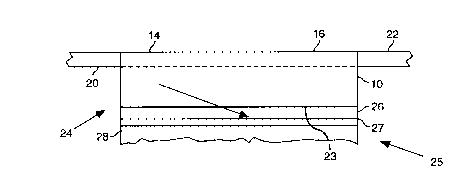
As shown in F~G. 3A, an antireflective optical absorbing device 25
according to the present invention may be formed by depositing an absorbing
-6-
CA 02240117 1998-06-08
layer 26 on the MIOC 12 and then attaching the mount 28 to the absorbing
layer 26. The mount 28 may be formed of SiO2. The absorbing layer 26
preferably is formed of SnTe, which is a semiconductor that is often used as a
tertiary compound with lead (i.e. PbSnTe) to make adjustable bandgap
5 infrared detectors. SnTe has a refractive index n = 6.3 and an extinction
coefficient k = 1.09 at a wavelength of 1550 nm. The coating thickness of the
SnTe absorbing layer 26 for a wavelength of 1550 nm is 558 Angstroms. The
thickness of the absorbing layer 26 to achieve both antireflection and
absorption is a function of the optical wavelength.
The absorbing layer 26 is deposited on the bottom side 23 of the MIOC
substrate 12 opposite from the side on which the optical waveguides 14-16
are formed. An adhesive 27 with an index of refraction similar to that of the
mount 28 may be used to attach the coated MIOC to the mount 28.
F~G. S illustrates the reflection error, l-R (with R being the reflection
15 coefficient), versus angle of incidence. From FIG. 1 it may be seen that the
reflection ~ "" of 0.001 occurs at about 86~, as required to produce
illllllll reflection in the MIOC 12 having the dimensions given above. In
prior art devices some light having angles of incidence that differ from the
nominal value of 85.8~ is reflected to the output facets of the optical
20 waveguides 1~16. Therefore, it is an important feature of the present
invention that the angular range for low reflections is large enough to give
low reflection for incidence angles lower and higher than the nominal value of
86~.
-7-
CA 02240117 1998-06-08
Another consideration is the dependence of the sensitivity of the
coating 26 on its thickness. FIG. 6 shows the sensitivity of the AR coating 26
to thickness over a range departing +10% from the nominal thickness of 558
A. The thickness tolerance is seen to be within the capabilities of the present
5 coating systems.
The sensitivity of the coating 26 to refractive index is another factor
that must be considered in the design of the coating 26. FIG. 7 shows the
sensitivity of the coating 26 to refractive index. The graph of F~IG. 7 gives
the reflection error as a function of the percent deviation of the refractive
10 index from the nominal value of 6.3. The range of the horizontal axis in FIG. 7
is the nominal value +10%.
F~IG. 8 graphically illustrates the coating sensitivity to variation in the
extinction ratio over the same +10% range of the nominal parameter. Again
the sensitivity is not so critical that these parameters cannot be satisfactorily
15 controlled.
Since the SnTe coating 28 has excellent absorption and low scatter it
will result in a large extinction ratio improvement relative to partially
absorbing (e.g. carbonblack) coatings on trenches or on roughened finishes
which scatter quite profusely.
CA 02240117 1998-06-08
Principle of Operation
In the following explanation of the operation of the invention, the
MIOC substrate 12 is referred to as the ambient medium because this is the
medium in which the light propagates before being incident upon the
5 absorbing layer 26. The MIOC substrate 12 is designated by the subscript
"A." The layer 26 is designated by the subscript "L." The medium 28 (shown
as semi-infinite) upon which the coated MIOC is mounted is referred to as the
substrate 28 and designated by the subscript "m."
The coating 26 is similar to a single layer quarter wave antireflective
10 coating but with one important additional requirement: the design must be
such that no light is transmitted into the mount 28 opposite from which the
light approaches. This latter condition can be satisfied by choosing the
substrate 28 index, nm such that total internal reflection will occur at the
interface between the layer 26 and the mount 28.
The design of a standard 1/4 wave antireflective layer is described
below. The refractive index of the layer is
nL = ~ (1)
where nA is the refractive index of the ambient medium (the MIOC substrate
12) from which the light approaches the antireflective layer 26S. This choice
20 of antireflective layer refractive index provides the same reflection at the
ambient-layer (AL) interface as at the layer-mount interface (LM). Therefore,
_g_
CA 02240117 1998-06-08
the amplitude of the light returning from the AL interface is the same as the
amplitude of the light reflected from the LM interface. The 1/4 wave layer
thickness has a round trip length of 1/2 half wavelength, which causes the
phase of light from the LM interface to be 180~ from that of the ambient layer
5 interface. The phase difference results in complete cancellation of the two
interface reflections. Therefore, there is no reflection of the selected
wavelength from the entire system.
In the present invention, there is no transmission through the mount 28.
Therefore, the refractive index of the mount 28 is chosen for total internal
10 reflection so that all of the light will be reflected from the LM interface.
Therefore, if there were only very small absorption in the layer 26, the
reflection at the AL interface would have to be 50% in order that the
remaining transmitted 50% of the light that comes back from the layer-
substrate interface 180" out of phase could be canceled to achieve
15 antireflection. Recall from Snell's law of refraction that the incidence angle in
the semiconductor layer is quite small by virtue of its high index of refraction.
The intensity throughput in one round trip in a quarter wave layer is then
approximately
-27lk
T~ = e nL (2)
-10-
CA 02240117 1998-06-08
where the semiconductor index, nL, is 6.3 and the extinction ratio k is about
1.0 so that Tl~4 = e~l= 0.37. Therefore, the reflection, RAL7 Of the AL interface
need be only
RAL = Tl TAL
S where TAL is the intensity transmission of the AL interface.
Eq. (3) shows that it is possible to trade off the k and n of the layer
since R and T are more strongly related to n while Tl~4 is more strongly related
to k. This tradeoff provides greater freedom in selection of materials for the
layer 26 and the mount 28.
For simplicity, the requirements for index of the layer 26 have been
described as if the incidence angle were 0~. When the incidence angle is
non-zero, then an effective index concept may be used. The effective index
for TM light (p-polarized) is
neff = c s ~3 (4)
15 where O is the angle of the light ray with respect to the interface normal. For O
= 86~ with n = 2.2, n effective iS about 30, which is much larger than the index n
= 2.2 for the mount 28. The refractive indices nA and nm in Eq. (1) should be
converted to their effective values using Eq. (4). Then Eq. (1) results in the
-11-
CA 02240117 1998-06-08
effective value of nL, which should be converted from its effective value again
using Eq. (4).
It should be pointed out that, if appropriate layer n and k can still not
be found, then as illustrated in FIG. 3B, one may make a symmetric three layer
S quarter wave stack 40, where the first and third layers have a high index of
refraction, nH, and the middle layer has a lower index of refraction, nLOW. This
is an effective quarter wave layer, the so-called Herpin equivalent layer
(HEL). At normal incidence, the effective index of refraction of this stack is
neffO = nH / nLow -
At non-normal incidence, Eq. (4) must again be applied. For normal
operation, all of the layers in the HEL must have refractive indices large
enough that total internal reflection does not occur. Even so, it will be
understood that application of Eq. (S) provides greater freedom in selection of
materials that will satisfy the requirement given above for n and k.
The structures and methods disclosed herein illustrate the principles of
the present invention. The invention may be embodied in other specific forms
without departing from its spirit or essential characteristics. The described
embodiments are to be considered in all respects as exemplary and illustrative
rather than restrictive. Therefore, the appended claims rather than the
20 foregoing description define the scope of the invention. All modifications to
the embodiments described herein that come within the meaning and range of
equivalence of the claims are embraced within the scope of the invention.