Note: Descriptions are shown in the official language in which they were submitted.
CA 0224023~ 1998-06-10
FMC 0880 PUS
MULTILAYER ELECTRICAL INTERCONNECTION
DEVICE AND METHOD OF MAKING SAME
Technical Field
This invention generally relates to
multilayer electrical interconnection devices. More
specifically, the present invention relates to a
multilayer electrical interconnection device which is
capable of bonding ceramics and metal multilayers to
non-roughened aluminum substrates with the use of
thermal spray technology.
Backqround Of The Invention
The use of circuit boards in manufacturing
electronic equipment provides many advantages,
including a reduction in the space and weight
required, increased reliability, and suitability for
automated production. A circuit board comprises an
insulating layer, carrying conductive metal traces,
and bonding locations for electrical components. Due
to advances in electronics, particularly in the area
of miniaturization of integrated circuits, the need
for multilayer boards has increased to facilitate the
increased number of circuit interconnections per unit
of surface area on a circuit board.
These multilayer circuit boards are designed
to replace the conventional printed circuit board
modules within which electrical connections are made.
Conventional printed boards are housed in cast
aluminum to provide the heat evacuation needed during
service. Multilayer circuit boards utilize separate
trace patterns on various layers in three dimensions
and layer-to-layer interconnects (i.e., vias or plated
CA 0224023~ 1998-06-10
throughholes) to implement complex interconnections in
a small space.
The creation of such a multilayer circuit
board, however, depends on adequate bonding of each
layer to the adjacent one, and the electrical and
mechanical properties of the layers. Until now, the
principal bonding technique has required roughening of
the cast aluminum surface to effectuate bonding. Such
roughening has been carried out by mechanical means
such as grit blasting, high pressure water, electric
discharge machining or chemical etchants. However,
such techniques are problematic due to the cost and
extent of disruption of the substrate and/or the
environment required. Accordingly, there exists a
need for a method of bonding multilayers to a
substrate without mechanical roughening.
From a bonding standpoint, aluminum and
aluminum alloys are generally very reactive and
readily form intermetallic alloys with nickel,
titanium, copper and iron at moderate temperatures.
To offset such reactivity, aluminum or aluminum alloys
form a passivating surface oxide film when exposed to
the atmosphere at ambient temperatures. This oxide
film inhibits adherence of metals and ceramics to non-
roughened aluminum. Thus, to effect a metallurgical,chemical or intermetallic bond between aluminum or
aluminum alloy and other metals and ceramics, it is
often necessary to remove, dissolve or disrupt the
oxide film. Once stripped of the oxide, aluminum or
an aluminum alloy will readily form an alloyed bond at
temperatures as low as 500~ C.
To this end, fluxes are readily used to
achieve oxide film stripping. One such example
involves brazing two pieces of aluminum alloy sheet
CA 0224023~ 1998-06-10
--3--
metal which are joined by assembling the pieces in a
jointed relationship and then flooding the joint area
with a flux applied at room temperature. When heated
aggressively, the flux melts and strips the surface
oxide, thereby allowing the layer to form an
interfacial alloy joint with the aluminum (see U.S.
Patent 4,911,351). Such fluxing techniques while
effective with rolled aluminum sheet, fail to function
with cast aluminum alloys. Since cast aluminum is
porous, non-homogenous and has a melting temperature
which may overlap with the melting temperature of the
flux, fluxing is not a suitable technique for oxide
stripping of cast aluminum alloys, except when
additions are made to the flux that reduces its
activation temperature.
Accordingly, there is a need for a method of
bonding each layer of a multilayer circuit board to
the adjacent one, including a method of bonding
multilayers to a metal substrate without roughening.
Summar~ Of The Invention
An object of the present invention is to
provide a method of bonding ceramic and metal
multilayers to non-roughened aluminum surfaces.
Another object of the present invention is to provide
a method of bonding which prevents the formation of
galvanic couples between the substrate and any
intermediary coatings. Yet another object of this
invention is to create a rough aluminum substrate
surface for bonding ceramic coatings to metals.
In carrying out the above objects, a method
is disclosed for bonding a thermally sprayed coating
to a non-roughened aluminum substrate including the
CA 0224023~ 1998-06-10
following steps: a) cleaning the substrate such that
the substrate is substantially devoid of grease and
oil; b) depositing a flux material on the substrate to
provide a dry flux coated substrate, wherein the flux
is capable of removing metal oxides on the metal
substrate; c) thermally activating the flux on the
flux coated substrate to melt and dissolve any metal
oxide residing on the coated aluminum substrate; and
d) subsequent to the step of thermally activating,
thermally spraying aluminum onto the flux coated
substrate by spraying to form a coating that is
chemically bonded to the aluminum substrate.
This invention also discloses a method of
bonding a thermally sprayed coating to a non-roughened
aluminum substrate, which includes the step of
thermally spraying aluminum onto a flux coated
substrate with an aluminum powder to form a coating
that is mechanically bonded to the substrate.
Brief Description Of The Drawinqs
Figure 1 is a generalized schematic diagram
illustrating the thermal spray apparatus used in
accordance with the invention;
Figure 2 is a table which illustrates the
roughness of various layers sprayed to produce a
circuit board, such as a) an uncoated and unfluxed
substrate, b) the aluminum spray on a fluxed and
activated substrate, c) the first ceramic layer, d)
the copper trace, e) the second ceramic layer, f) the
second copper trace, and g) the third ceramic layer;
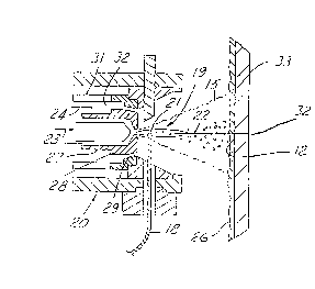
Figure 3 is a highly enlarged sectional view
of a portion of a spray gun on an aluminum substrate;
CA 0224023~ 1998-06-10
Figure 4 is a microphotograph depicting an
aluminum fluxed substrate and a three-layer coating
structure; and
Figure 5 is a microphotograph depicting a
seven layer circuit board.
Detailed Description Of The Invention
A multilayer electrical interconnection can
be achieved through thermal spray methods. Figure 1
shows a thermal spray apparatus for generating a
thermal spray to selectably deposit insulating and
conducting material to manufacture an interconnect
device. A thermal spray comprised of carrier gases
and particles of selected materials is formed by
heating particulates using an electric arc or chemical
combustion as a heat source. Layered structures are
formed by alternately spraying insulating and
conducting particles in predetermined patterns.
As depicted in Figure 1, a thermal spray
nozzle 10 receives material to be deposited from
supply bins 11 and 16. The flow of material into
nozzle 10 is selectably controlled using feeder valves
13 and 14, respectively. One bin may contain
particles of a conducting material while the other
contains particles of an insulating material.
Particles are heated, propelled by a carrier gas and
directed out of nozzle 10 as a thermal spray 15 for
deposition. Thermal spray lS is directed toward the
substrate 12 where the desired interconnect device is
to be fabricated.
Three-dimensional circuity is formed by
sprayed multilayers which are connected via the use of
positive and negative masks that produce localized and
CA 0224023~ 1998-06-10
-6-
well defined points of conductive and insulating
junctions in the board. Creation of a such a
successful multilayer structure depends on adequate
bonding of each coating layer to the adjacent layer,
and ensuring that the coatings are reliably bonded to
the substrate.
One such method to reliably bond the
coatings to the substrate involves roughening the
substrate by water jet or grit blasting. However,
both of these techniques are undesirable in a high
volume manufacturing environment. In answer to this
problem, Ford has developed a method of bonding
thermal spray coatings to non-roughened aluminum
surfaces involving the use of metallic coatings in
combination with bond coats such as nickel,
aluminides, silicon bronze or aluminum bronze to
induce metallurgical bonding of the coatings to the
substrate. However, with certain applications, the
method of bonding thermal spray coatings to non-
roughened surfaces, using metallic coatings, createsthe possible formation of galvanic couples between the
substrates and the coatings. Moreover, with respect
to ceramic coatings, since ceramic cannot
metallurgically bond to metals, an alternate boding
technique is required. The present invention thus
describes the additional steps which need to be taken
to apply a spray method to bond ceramic and metal
multilayers to metal substrates without the need for
mechanical roughening and to prevent the formation of
galvanic couples.
The present invention thus describes a
technique for roughening an aluminum substrate such
that ceramic coatings can bond to metals by
intercalating an intermediate, metallurgically bonded,
CA 0224023~ 1998-06-10
-7-
metallic coating by spraying an aluminum coating that
bonds to a fluxed aluminum substrate and does not form
a galvanic couple with aluminum. While previous
thermal spray techniques are appropriate for metal to
metal multilayers, for ceramic to metal multilayers,
roughening of the metal substrate is required. In
addition, depending on the desired application, the
absence of galvanic couples may be important, such as
for creation of multilayer circuit boards.
To prevent the formation of galvanic couples
and to provide a surface suitable for ceramic bonding,
aluminum is thermally sprayed onto an aluminum
substrate. Since aluminum is thermally sprayed on an
underlying aluminum substrate, the formation of
galvanic couples is prevented -- as compared to the
deposition of other metals such as nickel and the like
to the aluminum substrate. In addition, the sprayed
aluminum on the aluminum substrate creates a surface
with sufficient roughness for bonding to a ceramic
layer.
The metal substrate is preferably prepared
by the following steps: (1) cleaning and degreasing
of the metal substrate such that the metal substrate
is substantially devoid of grease and oils. The
second step involves fluxing and drying of the metal
substrate.
This invention is preferably concerned with
successfully fluxing cast aluminum alloys, such as
319, 356, 380 and 390, that contain silicon, copper,
manganese or iron ingredients in amounts ranging from
0.5-5~ by weight, the latter aluminum alloys possess a
melting temperature of about 580-600~ C. The surface
roughness of these cast alloys is usually about 1-3 ~m
Ra which is insufficient by itself to provide a
CA 0224023~ 1998-06-10
mechanical interlock with thermally sprayed coatings
thereover. Since the reactivity of aluminum is
diminished due to the formation of oxide films on
their surface, the aluminum substrate is fluxed to
remove any oxide film therefrom which facilitates
adherence of ceramics to the fluxed aluminum
substrate.
Figure 2 is a table which provides a
comparison of the roughness values for the various
layers of a seven layer circuit board. Of particular
importance is the difference in roughness between the
unfluxed and uncoated aluminum substrate, having a
roughness of 0.4746 ~m, and the fluxed, activated and
aluminum-sprayed substrate, having a roughness of
22.2367 ~m. Following application and activation of
the flux material and subsequent aluminum spray, the
aluminum substrate has been altered to create a
surface with a roughness sufficient to facilitate
bonding of ceramic and metal layers thereon. A flux
material is thus applied to the aluminum substrate to
strip the substrate of any oxide films.
A flux material having a melting temperature
well below the melting temperature of the cast
aluminum alloy, i.e., about 60-80~ C below, is
deposited thereon and dried. The flux is selected
preferably to be eutectic comprising a double fluoride
salt having the phase formula ~. K3AlF6+KAlF4. Such a
eutectic contains AlF3 at about 45 mol percent of the
double fluoride salts, with KF being about 55 mol
percent. The eutectic has a melting temperature of
about 560~ C which is about 40~ C below that of the
melting temperature of the cast alloy of the
substrate. If the double fluoride salt has a
substantially different mol or percentage of AlF3, thus
CA 0224023~ 1998-06-10
_ g_
not being a eutectic, the melting temperature will
rapidly rise. Other double fluoride salts, and for
that matter other alkaline metal fluoride or chloride
salts, can be used as long as they have a melting
temperature that can be heat activated without
disturbing the cast aluminum alloy. Fluoride salts
are useful, but undesirable because they fail to
provide corrosion resistance on the aluminum product,
and may attack aluminum alloy grain boundaries.
To deposit the flux, the salt is dissolved
or suspended in a sprayable medium, such as water or
alcohol, in a concentration of about 0.5-5.0 ~ by
volume or minimum of 5 grams of flux per square meter
of surface. The solution may contain a mild alkaline
wash, such as the commercial chemical product 5896,
permitting the flux to spread more evenly by reducing
surface tension. This solution may also contain other
additional ingredients, such as up to 50 wt. ~ of LiF,
or CsF which facilitate working with other substrates
such as magnesium oxide films.
The double fluoride salt is added to the
sprayable medium and closely control particle size to
minimize the need for stirring and to retain at least
25~ by volume of the salt and suspension at all times.
To this end, the salt particle size is equal to or
less than 10 microns with about 70~ being 2-4 microns.
The salt is spray deposited in a density of about 3-7
grams per square meter, preferably about 5 grams per
square meter; too much salt will inhibit flux melting
and too little will fail to achieve the fluxing
effect.
Deposition is carried out preferably by use
of a liquid spray gun which applies the flux solution
in a controlled manner to achieve the desired coverage
' CA 0224023~ l998-06-lO
.
--10--
and coating uniformity. After deposition, the flux is
dried preferably by placing the flux coated substrate
in a dehumidifier and removing the solvent. This
leaves a fine talc-like powder on the substrate.
The next step involves thermal activation of
the flux and dried surface to its eutectic melting
temperature, i.e., 500-580~ C. In contrast to the
application of other metals, since molten aluminum has
a temperature of about 660~ C, which is less than the
melting temperature of the flux, a separate thermal
activation step of the flux is required. Thermal
activation of the flux can optimally be brought about
by independent means such as flame, induction, and
resistance heating. Thermal activation of the flux is
achieved by heating the flux to its melting point,
rendering it colorless.
The next step involves intercalating an
intermediate, metallurgically bonded metal coating by
thermally spraying pure aluminum onto the activated
surface using wire or powder feedstock. With respect
to wire thermal spray, the wire preferably has a
diameter of at least 2 mm, O. 062 inches, and the spray
gun parameters are preferably adjusted to produce
spray at a current of 100-150 amperes, with a voltage
of 20-25 volts, and projecting a gas pressure of 50-60
psi. With respect to powder spray systems, the
starting powder particle size distribution can be
judiciously chosen to produce the required droplet
size irrespective of the wire parameters. Under these
conditions, the absolute roughness Ra of the sprayed
surface is between 12 microns and 30 microns or, more
preferably, between 15 and 25 microns, a roughness
sufficient to chemically lock in place subsequent
ceramic and copper layers. When aluminum powder is
CA 0224023~ l998-06-lO
deposited, in the preferred embodiment, a single
plasma or flame thermospray gun is utilized to
activate the flux and also spray the aluminum powder
onto the aluminum substrate. Under this preferred
5 embodiment, the plasma gun operates with a voltage of
approximately 78 volts, at a current of 525 amps, and
with an argon gas flow rate of 27 cubic feet per hour.
The preferred aluminum particle size ranges from 10-75
~m. Accordingly, an intermediate layer is created,
having sufficient roughness to facilitate bonding the
ceramic and metal layers.
Thermal spraying of aluminum droplets or
particles can be carried out by use of an apparatus as
shown in Figure 3. A metallic wire feedstock 18 is
15 fed into the plasma or arc 19 of a thermal gun 20 such
that the tip 21 of the feedstock 18 melts and is
atomized into droplets by high velocity gas jets 23
and 24. The gas jets project a spray 15 onto the
substrate 12 and thereby deposit a coating 26. The
20 gun 20 may be comprised of an inner nozzle 27 which
focuses a heat source, such as the flame or plasma
plume 19. The plasma plume 19 is generated by
stripping off electrons from the primary gas 23 as it
passes between the anode 2 8 and the cathode 29
25 resulting in highly heated ionic discharge or plume
19. The heat source melts the wire tip 21 and the
resulting droplets 22 are carried by the primary gas
23 at great velocity to the target. A pressurized
secondary gas 24 may be used to further control the
30 spray pattern 15. Such secondary gas is introduced
through channel 30 formed between the cathode 29 and
the housing 31. The secondary gas 24 iS directed
radially inwardly with respect to the axis 32 of the
plume. Melting of the wire 18 is made possible by
CA 0224023~ 1998-06-10
.
connecting the wire as an anode when striking an arc
with cathode 29. The resulting coating 26 will
constitute splat layers or particles 33. While use of
the wire feedstock is described in detail, powder fed
thermal spray devices can also be used to produce the
same bonding effect.
Figure 4 shows a scanning electron
micrograph of a fluxed aluminum substrate. Figure
4(b) illustrates one application of this thermal spray
bonding method, to create a three layer circuit board,
composed of an aluminum, alumina and copper layer.
While we do not wish to be bound by any theoretical
reason, the bonding achieved in this invention can be
attributed to intermetallic alloy formation and/or
pairing of oxygen atoms located at the hot droplet
surfaces with the oxide free aluminum surface.
Figure 5 is a scanning electron micrograph
of yet another application of the bonding method to
create a seven layer circuit board. As depicted, the
seven layer circuit board is composed of several
layers bonded to one another with the following layer
structure: aluminum, alumina, copper, alumina, copper,
alumina and copper.
The present invention thus facilitates
bonding of ceramics and metals to non-roughened
aluminum substrates to form multilayer structures.
While the best mode and viable alternate
embodiments for carrying out the invention have been
described in detail now shown on the drawings, those
familiar to the art to which this invention relates
will recognize various alternative designs and
embodiments for practicing the invention as defined by
the following claims.