Note: Descriptions are shown in the official language in which they were submitted.
CA 02240351 1998-06-11
PIPELINED SNOOPING OF MULTIPLE L1 CACHE LINES
Background of the Invention
Technical Field of the Invention
This invention generally relates to caches for computer systems, such as set
associative
caches and direct-mapped caches, and more particularly to reducing snoop busy
time.
Background Art
The use of caches for performance improvements in computing systems is well
known
and extensively used. See, for example, U.S. Patent 5,418,922 by L. Liu for
"History
Table for Set Prediction for Accessing a Set Associative Cache", and U.S.
Patent
5,392,410 by L. Liu for "History Table for Prediction of Virtual Address
Translation for
Cache Access".
A cache is a high speed buffer which holds recently used memory data. Due to
the
locality of references nature for programs, most of the access of data may be
accomplished in a cache, in which case slower accessing to bulk memory can be
avoided.
In typical high performance processor designs, the cache access path forms a
critical path.
That is, the cycle time of the processor is affected by how fast cache
accessing can be
carried out.
EN9-96-038 1
CA 02240351 1998-06-11
A typical shared memory multiprocessor system implements a coherency mechanism
for
its memory subsystem. This memory subsystem contains one or more levels of
cache
memory associated with a local processor. These processor/cache subsystems
share a bus
connection to main memory. A snooping protocol is adopted where certain
accesses to
memory require that processor caches in the system be searched for the most
recent
(modified) version of requested data. It is important to optimize this
protocol such that
interference as seen by local processors is minimized when snooping occurs. It
is also
important to move data out of the cache as quickly as possible when a memory
access is
waiting for cache data resulting from a snoop.
In accordance with an exemplary system, a two level cache subsystem with level
2 (L2)
cache line size some power of 2 larger than level 1 (L 1 ) cache line size is
implemented.
Both caches implement writeback policies, and L 1 is set-associative. L 1 is
subdivided
into sublines which track which portions of the cache line contain modified
data. The
cache subsystem implements mufti-level inclusion wherein all blocks resident
in L 1 must
also be resident in L2. Snoop requests from the bus are received at L2 and, if
appropriate,
the request is also forwarded on to L 1. The snoop request forwarded to L l,
however,
requires accessing the L 1 directory for all of the consecutive L 1 cache
entries which
may contain data associated with the L2 cache line. Each directory access is
sent to the
L 1 cache subsystem as an individual request. Each cache read access resulting
from a
directory access waits for cache directory information which indicates slot
hit and subline
offset. Slot hit information can be used in parallel with the cache access but
the subline
offset is used to generate the address in the cycle before the cache read.
Referring to Figure 7, an example is given where a single forwarded L2 snoop
request
requires two L 1 directory accesses. Two data transfers out of L 1 are
required for each
EN9-96-03 8 2
CA 02240351 2001-02-09
directory access because both L 1 lines have modified data in both of their
sublines. This
example demonstrates two problems with the design of this exemplary system.
( 1 ) The processor associated with the L 1 cache being snooped is prevented
from accessing
the L 1 cache subsystem when ei ther the L 1 directory or cache is being used
by a snoop
operation. This is illustrated by holding the processor pipe (cache busy)
through cycles 1
through 9. Use of these resources occurs in different cycles which extends the
overall busy time
for the snoop operation.
(2) Delay exists between the transfer of the first and second cache blocks
which in turn
delays when the memory access associated with the scoops can proceed.
It is, therefore, an object of the invc;ntion to reduce the number of cycles
required for an L1
snoop operation.
It is a further object of the invention to avoid delays between first and
second cache blocks which
cause delays in memory access associated with snoops.
Summary of the Invention
In accordance with the invention, an apparatus and method for operating a
computing system
including a cache includes accessing a directory for a second snoop request
while evaluating a
directory access from a first snoop request.
In accordance with a further aspect of the invention, an apparatus and method
is provided for
operating a computing system including a two level cache subsystem including
an Ll cache and
an L2 cache. During a REQUEST stage, a directory access snoop to the directory
of the L 1
cache is requested; and responsive thereto, during a SNOOP stage, the
directory is accessed;
during an ACCESS stage, the cache arrays are accessed while processing results
from the
SNOOP stage. These stages are fully overlapped in a pipelined fashion. If
multiple data
transfers are required out of the Ll cache, a pipeline hold is issued to the
REQUEST and SNOOP
EN9-96-038 3
CA 02240351 2001-02-09
stages, and the ACCESS stage is repeated. During a FLUSH stage, cache data
read from the L1
cache and during the ,ACCESS stage is sent to the L2 cache
In one aspect of the present invention there is provided a method for
operating a computing
system including a cache for executing a snoop operation comprising: executing
a request stage,
a snoop stage and an access stage; during said request stage, requesting
access to the directory of
said cache; during said snoop stage executed in a first clock cycle, accessing
the directory of said
cache; during said access stage executed in the next clock cycle following
said first clock cycle,
simultaneously accessing data arrays of said cache while processing the
results of said snoop
stage; and issuing a hold to said request and snoop stages if multiple data
transfers are required
out of said cache during said access stage.
In a further aspect of the invention there is provided a method for operating
a computing system
including a two level cache subsystem including an L 1 cache and an L2 cache
controller,
comprising the steps o~ during a R>=:QUEST stage, requesting a directory
access snoop to the
directory of said L 1 cache; and responsive thereto during a SNOOP stage,
accessing said
directory; during an ACCESS stage, accessing the data arrays of said L1 cache
while processing
results from said SNOOP stage; and iif multiple data transfers are required
out of said L 1 cache,
issuing a pipeline hold to said REQUEST and SNOOP stages; and repeating said
ACCESS stage;
and during a FLUSH stage, sending to said L2 cache controller the cache data
read from said L 1
cache during said ACCESS stage.
In a further aspect of the invention there is provided a computing system
including a two level
cache subsystem including an L 1 cache and a system device, comprising: means
for requesting a
directory access snoop to the directory of said L 1 cache during a REQUEST
stage; and
responsive thereto means for accessing said directory during a SNOOP stage;
means for
accessing said cache arrays during an ACCESS stage while processing results
from said SNOOP
stage; and if multiple data transfers are required out of said L1 cache, means
for issuing a
pipeline hold to said REQUEST and SNOOP stages; and means for repeating said
ACCESS
stage; and means for sending to said system device during a FLUSH stage the
cache data read
from said L 1 cache during said ACC'.E.SS stage.
EN9-96-038 4
CA 02240351 2001-02-09
In a further aspect of the invention tlhere is provided a computing system
including a cache for
executing a snoop operation, comprising means for executing a request stage, a
snoop stage, and
an access stage; means operable during said request stage for requesting
access to the directory of
said cache; means operable during said snoop stage executed in a first clock
cycle for accessing
the directory of said cache; means op erable during said access stage executed
in the next clock
cycle following said first clock cycle for simultaneously accessing the data
arrays of said cache
while processing the results of said snoop stage; and means for issuing a hold
to said request and
snoop stages if multiple data transfers are required out of said cache during
said access stage.
In a further aspect of the invention there is provided a program storage
device readable by a
machine, tangibly embodying a prol;ram of instructions executable by a machine
to perform
method steps for operating a computing system including a cache for executing
a snoop
operation, said method steps comprising executing a request stage, a snoop
stage, and an access
stage; during said request stage, requesting access to the directory of said
cache; during said
snoop stage executed in a first clock; cycle, accessing the directory of said
cache; during said
access stage executed in the next clock cycle following said first clock
cycle, simultaneously
accessing the data arrays of said cache while processing the results of said
snoop stage; and
issuing a hold to said request and snoop stages if multiple data transfers are
required out of said
cache during said access stage.
In a further aspect of the invention there is provided an article of
manufacturing comprising a
computer usable medium having computer readable program code means embodied
therein for
operating a computing system including a cache for executing a snoop
operation, the computer
readable program means in said article of manufacture comprising computer
readable program
code means for causing a computer to effect executing a request stage, a snoop
stage, and an
access stage; computer readable program code means for causing a computer to
effect during said
request stage, requesting access to thc~ directory of said cache; computer
readable program code
means for causing a computer to etfe~ct during said snoop stage executed in a
first clock cycle,
accessing the directory of said cache; computer readable program code means
for causing a
computer to effect during said access stage executed in the next clock cycle
following said first
clock cycle, simultaneously accessing; the data arrays of said cache while
processing the results
EN9-96-03 8 4a
CA 02240351 2001-02-09
of said snoop stage; and computer readable program code means for causing a
computer to effect
issuing a hold to said request and snoop stages if multiple data transfers are
required out of said
cache during said access stage.
In a further aspect of the invention there is provided a computer program
product or computer
program element for operating a computing system including a cache for
executing a snoop
operation, according to the steps of executing a request stage, a snoop stage,
and an access stage;
during said request stage, requesting. access to the directory of said cache;
during said snoop
stage executed in a first clock cycle. accessing the directory of said cache;
during said access
stage executed in the next clock cycle following said first clock cycle,
simultaneously accessing
the data arrays of said cache while processing the results of said snoop
stage; and issuing a hold
to said request and snoop stages if multiple data transfers are required out
of said cache during
said access stage.
Other features and advantages of this invention will become apparent from the
following detailed
description of the presently preferred embodiment of the invention, taken in
conjunction with the
accompanying drawings.
Brief Description of the Drawings
Figure 1 is a block diagram illustrating a typical microprocessor architecture
within which a
preferred embodiment of the invention is implemented.
Figure 2 illustrates how Figure 2A through 2D relate, while the latter are
block diagrams
showing the implementation of a preferred embodiment of the invention within
the
microprocessor of Figure 1.
Figures 3-6 are block diagrams illustrating the system and L2 cache bus
interfaces 11)1 and 103
of Figure 1, with Figure 3 generally illustrating the system data bus; Figure
4, the system bus
controls; Figure 5, the L2 cache data bus; and Figure 6, the L2 cache
controls.
EN9-96-03 8 4b
CA 02240351 1998-06-11
Figure 7 is a table illustrating a snoop operation in accordance with the
prior art.
Figures 8 and 9 are tables illustrating the timing of snoop operations of a
preferred
embodiment of the invention.
Figure 10 is a logic flow diagram illustrating the four stages implementing
the pipelined
L 1 snoop operation of the invention.
Detailed Description of the Invention
Part 1
Referring to Figure 1, the microprocessor architecture within which a
preferred
embodiment of the invention is implemented will be described
Microprocessor chip 100 is organized to interface system bus 102 and L2 cache
104, and
includes the following functional units: fixed point unit (FXU) 106, floating
point unit
(FPU) 108, load store unit (LSU) 110 , instruction unit (IU) 112, instruction
cache unit
(ICU) 114, data cache unit (DCU) 116, L2 cache control unit 118, processor
interface unit
(PIU) 120, clock distribution and control 122, and address translation unit
(ATU) 124. In
a multiprocessor environment, several processors 100 and their associated L2
caches 104
may interface system bus 102 over buses equivalent to bus 101, and share
access through
system bus 102 to main memory (sometimes referred to as L3 memory) 126.
The various functional units of microprocessor 100 interface over data,
address, and/or
control I/O pins, lines and/or busses as will be described hereafter. When
referring to a
figure, "line" can refer to either a single signal line or a collection of
signal lines (i.e., a
EN9-96-038 5
CA 02240351 1998-06-11
bus). Those functional units most pertinent to the invention, and which will
be described
in greater detail hereafter, include the load/store unit (LSU) 110, the data
cache unit
(DCU) 116, the L2 cache control unit (CCU) 118, and the address translation
unit (ATU)
124.
In broad overview, the functional units on chip 100 communicate as follows.
Clock
distribution and control 122 provides clocking signals to all functional units
on
microprocessor chip 100. System bus 102 interfaces to PIU 120 over
bidirectional bus
101, and thence over buses 105 with CCU 118. L2 cache 104 communicates with
CCU
118 over buses 103. CCU 118 communicates instructions with ICU 114 over buses
109,
with DCU 116 over buses 111, and provides address information to ATU 124 and
receives miss interface signals over buses 107. LSU110 and IU 112 provide
request
interfaces to ATU 124 and receive translation state information over lines 129
and 131.
ATU 124 provides translated addresses to ICU 114 over lines 115, and to DCU
116 over
lines 113. ICU 114 interfaces to instruction unit 112 over bus 119. DCU 116
provides
data to FXU 106, FPU 108 and LSU 110 over bus 121, and IU 112 provides
instructions
to FXLT 106, FPU 108 and LSU 110 over bus 123. LSU 110 provides data to DCU
116
over bus 125. FPU 108 provides and receives data to DCU 116 over buses 127 to
LSU
110, then across buses 125. Processor 100 accesses main memory 126 through
system
bus 102.
Microprocessor Core 100
Referring to Figures 2A through 2D, and Figures 3-6, the core of
microprocessor 100 will
be described. Figure 2A generally corresponds to load/store unit (LSU) 110,
Figure 2B to
address translation unit (ATU) 124, and Figures 2C and 2D to data cache unit
(DCU) 116.
EN9-96-03 8 6
CA 02240351 1998-06-11
Figures 3-6 generally correspond to L2 cache control unit (CCU) 118 and
processor
interface unit (PIU) 120.
Dispatch block 300 directs instructions from instruction unit 112 to the
DECODE stage
buffers of the various execution units 106, 108, 110, including on bus 301
(which is that
portion of buses 123 directed to LSU 110) to LSU pipeline buffer 302
The function of load/store unit 110 is to generate effective addresses on 64
bit wide bus
313 for load and store instructions and to serve as a source and sink for GPR
data.
During writes to cache 400, registers 314 and 316 hold the data and address,
respectively;
the effective address is on bus 313, and data select block 320 puts the data
out on bus 323.
During cache reads, data from cache 400 comes in on line 461, is latched in
register 330,
and from there sent on line 333 to general purpose registers 306 or to fixed
point unit 106.
The output of LSU pipeline buffer 302 is fed on line 303 to the LSU decode and
address
generation block AGEN 304, which contains the general purpose registers 306
and
address generation adders (not shown). The data output of decode block 304 is
fed on
lines 311 to data register 314 and thence on line 319 to data select block
320. The
address output of AGEN 304 is fed on lines 313 to EXECUTE stage buffer 316,
and on
bus 309 to real address MRU 430. AGEN 304 output also includes control line
307,
which it sets to indicate either real or virtual mode addressing to data cache
control block
470.
The outputs of buffer 316 are fed on lines 317 to data select block 320 and to
data cache
address register 408, DIR address register 414 and register slot MRU address
register
406. The output of register 408 is fed on line 409 to multiplexer 412. Data
select block
EN9-96-038 7
CA 02240351 1998-06-11
320 contains the data to be stored to data cache 400 from load store unit 110,
and this is
fed thereto on store data output lines 323 via multiplexer 432, lines 433,
align block 460,
lines 461, register 456, lines 457, and line 427 via multiplexer 426. Data
select block 320
also provides control signals to data cache controller 470 on lines 321. The
other inputs
to multiplexer 432 are ( 1 ) L2 corrected data 609 via multiplexer 426 and
line 427, which
is also fed to data cache 400, (2) bypass data to DC on line 621, and (3)
unaligned data
(aka store merging and correction) register 452 via lines 453 to line 427 via
multiplexer
426. Multiplexer 432 output line 433 is also fed via align block 460 and line
461 to
register 456 and thence via multiplexer 424 to L2 cache controller on line
425, along with
the output of castout buffer 450 on line 451. Align block 460 is, in this
embodiment, a
barrel rotator or shifter which aligns D cache 400 data to quad word
boundaries on reads,
and from multiplexer 432 to quad word boundaries on stores.
An effective address from instruction unit 112 on line 367 (a portion of lines
131 ) is
latched in register 364 and fed on line 365 to ITLB 358 and to the compare and
address
select block 356 at ISLB 354. Line 313 from AGEN 304 is latched in register
384, and
fed on line 385 to DTLB array 378 and compare and address select block 374 at
DSLB
376. In this preferred embodiment, DTLB 378 may be a standard design, such as
that
described by Liu, supra. Whereas the Liu TLB design is 32 bits wide, in this
preferred
embodiment a 64 bit wide TLB 378 is used.
Data select 320 output on line 325 is fed to PUTAWAY stage buffer 330, which
also
receives data on lines 461 from data cache 400 (via lines 401 and align block
460) for
LSU 110, and FPU 108 results on line 327 which is a portion of bus 127. The
output of
PUTAWAY stage buffer 330 is fed on lines 333 to a floating point register in
FPU 108,
special purpose registers 334 (among which are the timers), and general
purpose registers
EN9-96-03 8 8
CA 02240351 1998-06-11
306. Special purpose registers 334 output line 335 is fed back to data select
block 320
which allows the processor to read them. Line 333 carries the data for FPU 108
when
doing a fetch from cache 400.
The selected output of instruction segment look aside buffer (ISLB) 354 is fed
on lines
355 to comparator 362, along with the virtual address output of ITLB 358 on
lines 359.
ITLB real address output lines 361 are input to IC controls 350 (which
includes
instruction directory 352) and status information on line 361 is fed to ATU
controls 370.
The output of comparator 362 is fed on lines 363 to IC controls 350 and to ATU
controls
370. The output of DSLB 376 is fed on lines 377 to comparator 382, along with
the
output of DTLB 378 on lines 379. The output of comparator 382 is fed on lines
383 to
ATU controls 370 and DC control 470. DTLB 378 status output 381 is fed to ATU
controls 370 and DC control 470. ATU controls 370 outputs include control
lines 369 to
data cache controller 470, L2 address 371 and ATU write data 373. IC controls
350
output is L2 address line 351. Real address from DTLB 378 is fed on lines 381
to DC
address register 408 and directory address register 414.
Predicted real address MRU 430 output signals on line 431, representing the
predicted
read address bits 50:51, are latched in registers 410 and 416. The output of
data cache
address register 410 on line 411 is multiplexed with bits 50:51 of the output
of register
408 in multiplexer 412, and its output is fed on address lines 413 to data
cache 400. The
remaining bits of DC address register 408 are fed straight through on line 413
to data
cache 400. Similarly, the output of register 416 is fed on lines 417 to
multiplexer 436,
where it is multiplexed with bits 50:51 of the output of register 414 on line
415, and the
result fed on lines 437 to directory array 440. The output of register 414 on
line 415 is
also fed to address register 408.
EN9-96-03 8 9
CA 02240351 1998-06-11
The function of real address MRU 430 is to provide predicted real address bits
50:51 to
data cache 400 and directory array 440.
During the fetch stage, data cache 400 output 401 is fed to unaligned data
register 452
and align block 460, and thence on line 461 to registers 456 and 330. Line 401
contains
the data to be read from data cache 400 by the load store unit 110, snoop data
to the L2
cache controller 118, merge data for partial stores to the data cache 400, and
castout data
to castout buffer 450. Slot MRU 402 output line 403 controls the selection of
one of four
sets of data to load on bus 401 through a multiplexer (not shown) on the
output of data
cache 400.
The output of castout buffer 450 is multiplexed in multiplexer 424 with the
output of
register 452 on lines 453 and line 457 from DC putaway register 456, the
output
appearing on lines 425 to the L2 cache controller. The output of register 452
along with
DC putaway register 456 and L2 corrected data on line 609 is also fed to data
cache input
multiplexer 426, the output of which appears on lines 427 to data cache 400
and
multiplexer 432. The output of register 406 is fed on line 407 to slot MRU
402. Slot
MRU 402 output 403 is fed to data cache 400 where it controls a data
multiplexer which
selects the appropriate cache set (as taught by Liu, supra.)
Data cache (DC) control 470 receives inputs from directory array 440 on lines
441
(signifying a directory array hit or miss), from AGEN 304 on lines 307, data
select and
execute cycle control block 320 on lines 321, ATU controls 370 on lines 369,
and
comparator 3 82 on lines 3 83. Its output is fed to L2 address line 471, and
includes a
EN9-96-038 10
CA 02240351 1998-06-11
signal signifying a miss condition. Miss information is also sent to ATU
controls 370 and
PA controls (not shown) in LSU 110.
The function of data cache control 470 is to control the data flow
multiplexing into and
out of data cache 400 and send results to the load/store unit 110, address
translation unit
124, and L2 cache control unit 118, and also to control writing of data into
data cache
400.
Data directory 440 contains address tags to indicate if the contents of the
real address are
present in cache 400, and the status of the cache lines, whether modified,
shared, or
invalid. It also contains an LRU pointer for each congruence class, indicating
which
cache 400 line should be replaced.
Address translation unit (ATU) control 370 handles translations from effective
addresses
to virtual addresses to real addresses. It receives as inputs L2 corrected
data on line 353,
and provides TLB reload data output on lines 375 to instruction translation
lookaside
buffer (ITLB) 358, data translation lookaside buffer (DTLB) 378, ISLB 354, and
DSLB
376. With respect to look aside tables 354, 358, 376, 378, if a miss condition
is detected,
ATU sequencer 370 requests data (address and length) to L2 cache on bus 371
(Fig. 6.)
When L2 responds on bus 353 (Fig. 5), ATU examines the data to select data for
look
aside buffer 378, 376, 354, 358, as the case may be, or signals a translation
exception
back to the instruction unit. ATU controls 370 tracks segment and page table
updates and
sends them to L2 controls on line 371. Line 381 provides the real address to
the data
cache directory for comparison.
EN9-96-03 8 11
CA 02240351 1998-06-11
The effective address is compared in ISLB 354 comparator 356 with the virtual
address.
If these match, then a valid effective to virtual address translation exists
in buffer 354,
which transmits the virtual address on line 355 to compare block 362.
ITLB 358 is accessed by an effective address on line 365 from register 364 for
doing
virtual to real address translation. The address input to ITLB 358 is a
portion of the
effective address from IU 112 on lines 367. Comparator 362 compares virtual
addresses
on lines 355 and 359, and signals the result on line 363. Associated with each
virtual
address in ITLB array 358 is a real address. The signal on line 363 indicates
whether or
not the address on line 361 is valid.
DTLB 378 is accessed by an address from register 384. Comparator 382 compares
data
on lines 379 and 377, and signals the result on line 383. The signal on line
383 indicates
whether or not the address on line 379 is valid.
System Bus Interface 120
Referring to Figures 3 though 6, the system bus interface 120 and L2 cache
control unit
118 of Figure 1 will be further described.
Correspondence between the high level block diagram of Figure 1, and the more
detailed
illustration of the preferred embodiment in Figures 3 to 6, is as follows. Bus
101 of
Figure 1 corresponds in Figures 3-6 to system controls lines 559 at
driver/receiver 556,
system address lines 569 at driver/receiver 564, system data hi bus 513 at
driver/receiver
512, and system data low bus 517 at driver receiver 516. Bus 103 to L2 cache
104 of
Figure 1 corresponds to L2 cache address lines 691 out of driver 690, L2 tag
address line
EN9-96-03 8 12
CA 02240351 1998-06-11
693 out of driver 692, L2 tag data lines 697 at driver/receiver 694, and L2
cache data bus
645 at driver/receiver 644. ICU bus 109 of Figure 1 corresponds (from ICU) to
IC
request lines 351, and (to ICU) DOIC register 606 output lines 607, and bypass
to IC
multiplexer 616 on lines 617. DCU bus 111 of Figure 1 corresponds (from DCU)
to DC
request lines 471 and data cache write data bus 425, and (to DCU) to bypass to
DC
multiplexer 620 on lines 621 and data cache data out (DODC) register 608
output line
609. Address translation unit (ATU) input/output bus 107 of Figure 1
corresponds to
ATU request lines 371, ATU write data bus 373, and multiplexer 612 output
lines 353.
Referring to Figures 4 and 6, requests to L2 cache control 118 are latched in
address/command register 650 from ATU request lines 371, IC request lines 351,
DC
request lines 471, and on lines 567 from address in register 566, which
latches system bus
addresses on lines 565 from receiver 564. These address/command signals are
latched as
required in registers 650, 652 and 654 connected via lines 651 and 653. The
output of the
third register 654 is fed to controls block 660 on line 655. The output of
first stage
register 650 is fed on lines 651 to register 652, driver 690 to provide L2
cache address
signal 691, driver 692 to provide L2 tag address signal 695, ECC checking
circuit 684,
address comparator 664, controls block 660, cache controller (CC) snoop
address register
670, processor address registers CBPADR 674 and CBMADR 676, and address
multiplexer 680. ECC 684 output is fed on lines 685 to driver 694 to provide
L2 tag data
on lines 697. CBPADR address register 674 contains the address to the system
bus in the
event of a cache miss, the output of which is fed to multiplexer 680 on line
675.
CBMADR address register 676 contains the snoop address portion, and its output
is fed to
multiplexer 680 on line 677. Receiver 694 output from L2 tag data lines 697 is
fed on
lines 695 to L2 tag in register (L2TAGIN) 688 and thence on lines 689 to error
correction
code (ECC) block 686. The output of ECC block 686 is fed on lines 687 to
comparator
EN9-96-03 8 13
CA 02240351 1998-06-11
664, address registers 670, 674 and 676. The output of comparator 664 is fed
on line 665
to controls block 660. CCS address register 670 output line 671 represents the
data cache
snoop address. The output of address out multiplexes 680 is fed on lines 681
to address
out register 560, and thence on line 561 to the system address bus 569 through
driver 564.
The output of controls block 660 is fed on lines 663 to arbitration and
control block 552,
and on lines 661 to address/command register 658. Arbitration and control
block 552
receives control data from receiver 556 via lines 557, and provides output on
lines 555 to
controls block 660, and in the event of an L2 cache miss request out control
signals are
sent on line 553 through driver 556 to system controls bus 559. Another output
of
controls block appears on lines 661 to address/command register 658, the
output of which
appears on line 659 to multiplexes 672. Multiplexes 672 also receives input
from lines
653 and 655, and provides its output on lines 673 back to register 650.
Referring to Figure 5, ECC block 632, DOIC register 606, DODC register 608,
L2PD0
register 636, multiplexes 616 and multiplexes 620 each receive inputs from
data input
register 624 on bus 625. The output of ECC block 632 is fed on line 633 to L2
data out
register 638, and thence to driver 644 on line 639. The output of L2PD0
register 636 is
fed on line 637 to inpage buffer 646, the output of which is fed on line 647
to L2PDI
register 642 and ECC circuit 632. The output of L2PDI register 642 is fed on
line 643 to
DOIC register 606, DODC register 608, CCDI register 624, and to bypass
multiplexers
620 and 616. The output of multiplexers 620 and 616 represent bypass data, and
are fed
on lines 621 and 617 to the DC and IC, respectively. Data cache write data
line 425 is fed
to CMCD register 628 and CCDI register 624. The output of CMCD register 628 is
fed
on lines 629 to L2PD0 register 636, and castout buffers 602.
EN9-96-038 14
CA 02240351 1998-06-11
Referring to Figures 3 and 5, L2 cache data in from bus 645 is received at
receivers 644,
fed on line 649 to L2 data in register 640 and thence on lines 641 to ECC
circuitry 634
and bypass multiplexers 616 and 620. From ECC circuitry 634, L2 cache data in
is fed
on lines 635 to cache controller data in register (CCDI) 624, DOIC register
606 and
DODC register 608. DODC register 608 output 609 is fed to data cache unit 116
(Figure
1 ), DC bypass multiplexer 620, ATU multiplexer 612, and castout buffers 602.
The
output of DOIC register 606 is fed on lines 607 to instruction cache unit 114
(Figure 1 ),
ATU multiplexer 612, and castout buffers 602. Castout buffers 602 output on
lines 603 is
fed to data high output register 502 and multiplexer 520, the output of which
is fed on
lines 521 to data output registers 502 and 504.
In operation, registers 624 and 636 form a pipeline buffer to inpage buffer
646 and
register 642. Inpage buffer 646 caches a line from the system bus. Line 641
from L2
data in register 640 to bypass multiplexers 616, 620 allows the saving of a
cycle on cache
misses when error correction is not required. DOIC register 606 provides
corrected data
to instruction cache unit 114, and DODC provides corrected data to data cache
unit 116.
Either register may supply data to the ATU 124.
The normal path for routing L2 cache data is through register 640, ECC 634,
and DOIC
register 606 and DODC register 608.
Processor Interface Unit 120
Referring now to Figure 3, a more detailed description of processor interface
unit 120 of
Figure 1, and associated circuitry, will be provided. Figure 3 represents the
data flow
portion of PIU 120 and system bus 102.
EN9-96-03 8 15
CA 02240351 1998-06-11
System bus 102 data high bus 513 and data low bus 517 communicate through
driver/receivers 512 and 516, respectively with data high output register 502
on lines 503,
data high in register 506 on lines 515, data low out register 504 on lines
505, and data low
input register 508 on lines 519. Each of busses 513, 517 is capable of
handling eight
bytes of data, providing a 16 byte data bus. If the system is operating on
only eight bytes,
only one set of the input/output registers (such as 504, 508) is used.
System data input registers 508 outputs on lines 507 and 509, respectively,
are fed to
multiplexer 524 and thence, along with registers 506 on lines 507, on lines
525 to cache
control data in (CCDI) register 624 (Figure 5), which is the main data input
register of the
cache controller. Data input register 624 output is fed on bus 625 to
multiplexer 520.
Load/Store Unit (LSU) 110
Load/store unit (LSU) 110 functions to decode fixed point and floating point
loads and
store and cache management operations, and to send effective addresses and
storage
commands to the data cache unit (DCU) 116. LSU 110 also handles most move-to
and
move-from special purpose register (SPR) 334 instructions. In addition to
functioning as
a load/store unit, LSU 110 also controls instruction execution sequencing
after
instructions have been dispatched, through detection of most instruction
execution
interlocks, and the generation of resulting pipeline hold signals.
LSU 110 provides a six port register file 306, made up of four 32x18 register
array
macros, arranged as a 32x72 array with two write ports and four read ports.
This array
implements the 64-bit general purpose registers (GPRs) 306. GPR array 306 also
EN9-96-038 16
CA 02240351 1998-06-11
provides operands for fixed point unit (FXU) 106 decode stage (not shown) as
well as for
LSU 110. FXU 106 decodes its own instructions and generates requests to LSU
110 for
the necessary operands, as well as providing on line 327 a result operand and
address
when appropriate. LSU 110 accesses GPRs 306 for registers needed to generate
effective
addresses (EA), and for data for store instructions. Data operands received
from data
cache 116 on line 461, and updated effective addresses are written back to the
GPRs by
LSU 110. Lines 327 contain the FPU results, and are fed to register 330.
In handling floating point loads and stores, LSU 110 generates effective
addresses using
operands from GPR 306, and accesses the necessary floating point register
(FPR)
operands from the floating point unit (FPU) 108.
Instructions dispatched to LSU 110 are latched in its DECODE cycle instruction
register
302 at the end of the I-fetch cycle. The basic LSU 110 pipe is three stages:
DECODE
302/304, EXECUTE 316/320, and PUTAWAY 330. During the DECODE cycle
corresponding to 302/304, the instructions are decoded, and operands are
fetched from the
GPR 306 array. Addressing operands are gated to a 64-bit address generation
(AGEN)
adder, and a 64-bit effective address is calculated. The effective address
(EA) is sent on
lines 313 to the address translation unit (ATU) 124 and to data cache unit
(DCU) 116 and
latched at the end of the DECODE cycle in pipeline buffer 316 which holds the
effective
address during the EXECUTE cycle.
During the EXECUTE cycle, the operand for store operations is passed to the
DCU on
line 323, where it is aligned in block 460 and saved in register 456 for
PUTAWAY in
D-cache 400. At the end of the EXECUTE cycle, if a load type instruction is
being
EN9-96-038 17
CA 02240351 1998-06-11
executed, the data operand returns on line 461 to LSU 110 from the DCU, and is
saved in
pipeline buffer 330 for PUTAWAY.
During PUTAWAY cycle 330, as is represented by lines 333, up to two 8-byte or
one
16-byte operand may be written to GPR 306. Floating point loads are limited to
one
8-byte operand per cycle. GPRs 306 are not written until late in the PUTAWAY
cycle
330. This requires that operands being written to these arrays be bypassed
around the
arrays to reduce pipeline interlocks. Delaying the write to GPR 306 also
allows sign
extension for algebraic load operations to be performed, helping to balance
path delays
between EXECUTE 316/320 and PUTAWAY 330 cycles for these instructions.
Fixed Point Unit (FXU) 106
Fixed point unit (FXL1) 106 executes the fixed point instructions, not
including storage
access instructions. FXIJ 106 includes a 64-bit adder, a 64-bit logical unit,
a 64-bit
rotate-merge unit, and a 64-bit carry save adder which supports two-bit-per-
cycle product
formation during multiply instructions.
During division, quotient formation occurs one bit per cycle, through repeated
subtraction
of the divisor from the shifted dividend.
Floating Point Unit (FPU) 108
Floating point unit (FPU) 108 executes the floating point instructions, but
not the storage
access instructions. In one exemplary embodiment, FPU 108 includes a 5-port
32x72-bit
register array, a 32-bit status-control register, a 3-bit overlap scan booth
encoder unit,
EN9-96-03 8 18
CA 02240351 1998-06-11
2-bit quotient generation unit, a 106-bit carry save adder, a 106-bit
increment-full adder,
an operand alignment shifter unit, a normalizer unit, and a rounder unit.
Address Translation Unit (ATU) 124
Referring, primarily, to Figure 2B, address translation unit (ATU) 124
translates the data
effective address (EA) from load/store unit (LSU) 110 and the instruction
effective
address from instruction unit 112 into real addresses used by the data and
instruction
caches to access their L 1 caches and used by the L2 cache control unit 118 to
access the
L2 cache 104.
Microprocessor 100 implements segment lookaside buffers (SLB) 354, 376 and
translation lookaside buffers (TLB) 358, 378, which function as caches for
segment and
page table entries. When a required entry is not found in a look aside buffer,
ATU 124
initiates a fetch to L2 cache control 118 to access segment and page table
entries from
memory 126 or L2 cache 104.
ATU 124 reports any translation data storage interrupts (DSI) to the
load/store unit 110
and any translation instruction interrupts to the instruction unit 112.
Reference, change
and tag change bits are all updated by store requests to cache control 118
from ATU 124.
Microprocessor 100 provides a 4-entry SLB 354 for instruction address
translation and an
8-entry SLB 376 for data address translation. SLBs 354, 376 contain the most-
recently
translated segments in a fully associative arrangement. The ESID (Effective
Segment ID)
portion of the effective data or instruction address is compared 356, 374
simultaneously
EN9-96-038 19
CA 02240351 1998-06-11
to all entries in the respective SLB 354, 376 ESIDs when segment translation
is enabled.
ATU 124 includes separate instruction and data TLBs 358, 378, respectively, to
hold the
results of virtual to real address translations. With virtual to real
translation active, the
VSID from the matching SLB 354, 376 is compared in comparators 362, 382
against the
VSID stored in the TLB 358, 378. If a compare is found, the Real Page Number
(RPN)
stored in the matching TLB 358, 378 entry is used to form the real address.
Replacement
is managed independently in each TLB 358, 378 by an LRU bit for each of the
256 pairs
of entries.
L1 Data Cache Unit (DCU) 116
In a preferred embodiment, L 1 data cache unit (DCU) 116 has the following
attributes: 64
KB size, 64 byte line size, 4-way set-associative, 2 subline-modified bits per
line, MRU
slot selection, 40-bit real address, 16-byte dataflow to/from processor, store-
in design,
and mufti-processor support. The term "cache line" refers to a 64-byte block
of data in
the cache which corresponds to a single cache directory entry. Slot MRU 402
provides
selection of one of four sets of cache data during an execute cycle. Real
address MRU
430 supplies bits 50:51 to cache 400 and cache directory 440. Error correction
ECC (not
shown) is provided on cache 400 and cache directory 440. Write-thru mode is
implemented.
The data cache 116 array 400, representing a collection of sub arrays, is
based on a
1024x78 1R1W "virtual" 2-port array macro. It provides for a read operation
followed by
a write operation within a processor cycle. Read data remains valid on the
array outputs
until the next read operation begins even if there is an intervening write
operation. Eight
EN9-96-038 20
CA 02240351 1998-06-11
of these arrays are used to form a 64KB cache 400. Two arrays are used per
slot to form
a 16-byte dataflow in and out of the array, represented by lines 401. Data
parity is stored
in the array. The last bit stored in the array is odd address parity across
bits 50:59 of the
address used to access the data cache.
Two arrays are needed to implement data cache directory 440. The directory
implements
a 28-bit real page number (RPN) along with five ECC check bits. A valid and
two
subline modified status bits are maintained, and three check bits are stored
with them.
The RPN and status fields are replicated four times to represent the four sets
accessed at a
particular directory array address. A 3-bit LRU is shared between two
directory arrays to
indicate the least recently used slot.
Slot MRU 402 logically appears as a 1024x4 array where each entry is
associated with a
cache line in data cache 400. Bits 48:51 of the 48:57 used to access the
logical array 400
are effective address bits. MRU 402 bits are updated whenever an incorrect
slot guess or
a cache miss occurs.
Real address (RA) MRU 430 is used to generate a prediction of real address
bits 50 and
51 for addressing both cache 400 and cache directories 440. As is represented
by line
309, array 430 is read as part of the AGEN stage 304 of the pipeline. If a
load/store unit
pipeline EXECUTE stage or latched PUTAWAY stage hold is present, then the
array 430
output is not used. Real mode is also used to determine if the array 430
(Figure 2C)
output is used. Real mode determination occurs in AGEN 304 which sets control
line 307
to either the real or virtual mode addressing. If real mode is determined,
then load/store
effective address (LSEA) 317 bits 50:51 are used by register 408 to access
cache 400 and
register 414 to access cache directory 440 instead of RA MRU array 430 output.
EN9-96-038 21
CA 02240351 1998-06-11
Real address (RA) MRU array 430 is updated from DC address register 408 via
lines 281
whenever a wrong prediction occurs with respect to translated address bits
50:51. Also,
data cache address register 408 and data cache directory address register 414
are updated
with proper values of address bits 50:51 via line 381 for reaccessing the
cache 400 and
cache directory 440 arrays. Multiplexor 412 is then switched under control of
data cache
control block 470 so that address register 408 is used to access cache array
400. A similar
function occurs with multiplexer 436 so that register 414 is used to access
the directory
array 440. The LSU 110 pipeline is stalled for one cycle to allow cache 400
and directory
440 to be reaccessed in parallel in the same cycle. Data is then returned to
LSU 110 via
line 461 in the following cycle.
Instruction Cache Unit (ICU) 114
Instruction cache unit (ICU) 114 contains the physical arrays, address
compares, and error
checking circuitry to provide a 64KB 4-way associative instruction cache with
single-bit
error detection and recovery. The single-cycle cache access provides up to
four
instructions from a selected 128-byte cache line. Instruction cache unit 114
provides
instructions to other functional units, including branch prediction.
L2 Cache Control Unit 118
The functions of the L2 cache control unit 118 are to provide processor 100
with access to
a private L2 cache 104, plus access to memory 126 through system bus 102 which
also
supports memory coherence control for multiprocessor operations. L2 cache 104
is
EN9-96-038 22
CA 02240351 1998-06-11
implemented as external static R.AMs, with one set of SRAMs for the directory
and
another set for the data.
CCU 118 accepts commands from four sources: data cache unit 116, instruction
cache
unit 114, address translation unit 124, and system bus 102 via processor
interface unit
(PIU) 120. To handle these commands, CCU 118 uses the buffer structure shown
in
Figure 6. External and internal commands are prioritized by CCU controls 660
and
placed into ADR/CMD buffer 650. ADR/CMD buffer 650 output 651 is then used to
access an L2 directory (not shown) via interface lines 693 driven by driver
circuits 692 to
determine the hit/miss status. Additionally, appropriate address bits from bus
651 are
concurrently used to access an L 1 status array (not shown) in controls 660 to
determine if
a data cache snoop needs to be done. Finally, ADR/CMD buffer 650 is used to
control
updating status and tag information in the L2 directory as required, a process
well
understood in the art.
The four L2 hit/miss states are:
1 ) Modified - This line is different from memory and no other coherent cache
has a copy
of this line.
2) Exclusive - This line is the same as memory and no other coherent cache has
a copy
of this line.
3) Shared - This line is the same as memory and other caches may have a copy
of this
line.
EN9-96-038 23
CA 02240351 1998-06-11
4) Invalid - This cache and this processor's data cache do not have a copy of
this line.
Data can be in the data cache only if it is also in the L2 cache.
Commands only stay in ADR/CMD buffer 650 for three cycles, at which time the
command moves to ADR/CMD buffer 652 or ADR/CMD buffer 658. A processor
command is moved into the ADR/CMD buffer 652 when said command is in ADR/CMD
buffer 650 and the resources it needs, such as the data flow, are not
available. The
command will stay in ADR/CMD buffer 652 until the resource becomes available.
Commands are moved to the ADR/CMD buffer 658 from ADR/CMD buffer 650 by way
of controls block 660 when a system bus snoop command needs to use the data
path. The
command will stay in ADR/CMD buffer 658 until the data path is available.
Commands
that need to issue address commands on the system bus are placed in ADR/CMD
buffer
654. The command will stay in ADR/CMD buffer 654, being retried if necessary,
until a
successful address status and response is received from system bus 102. If
data
movement is required the command is then turned over to the CCU data flow
logic.
Feedback from ADR/CMD buffer 658 to ADR/CMD buffer 650 is necessary for two
separate functional operations. The first feedback case is for processor read
commands
that encountered a shared address response from system bus 102. When the
processor
read command is first in the ADR/CMD buffer 650 the L2 directory is marked
exclusive,
assuming that this L2 will have the only copy of the data. If another device
indicates that
it also has a copy of this data, by a shared address response on system bus
102, then the
L2 directory must be changed from exclusive to shared.
EN9-96-03 8 24
CA 02240351 1998-06-11
The second feedback operation is used for processor write operations that must
wait for a
successful system bus 102 address status and response before the data can be
written. For
processor stores or data-cache-block-zero (dcbz) instructions that hit shared
in the L2
directory, the processor must make sure that it holds the line in the
exclusive state before
it updates the data. Before the processor can get ownership of the shared line
it may lose
the line to another device, so the feedback path is provided to reinitiate the
directory
access.
L2 Cache Control Unit Snoop Operations
Snoop commands from system bus 102 come in through processor interface unit
120 and
are presented to ADR/CMD buffer 650 via bus 567. At the same time a shift
register (not
shown) is started. The shift register is used to 'time out' the snoop command.
Snoop
commands require a response within a fixed time, but the command may be
delayed
before being brought into ADR/CMD buffer 650 because of other higher priority
commands. If the shift register 'times out', an address retry response will be
issued to the
system bus 102.
When a snoop command is accepted into ADR/CMD buffer 650 the L2 directory and
L 1
status array are checked. If the command hits in the L2 directory and the L 1
status array,
then a snoop command is issued to the data cache. If data must be moved to
complete the
snoop command, it will be first moved out of the L2 cache into the castout
buffer 602.
Then if the data cache has a modified copy of the data, its copy of the data
will be moved
to the castout buffer 602 and subsequently via bus 603 to system bus 102.
EN9-96-03 8 25
CA 02240351 1998-06-11
The memory management policy is such that segment and page translation table
entries
may not be accessed directly from the L1 data cache by the ATU 124.
Consequently,
another type of snoop operation is done for ATU commands. When an ATU command
comes in, the data cache is snooped using the L 1 status array. If the data
cache has
modified data, the ATU command is stopped until the data is moved from the
data cache
to the L2 data RAMs.
Processor Interface Unit (PIU) / Bus Interface Unit (BIU) 120
Referring to Figures 1 and 3, processor interface unit (PIU) 120 controls and
monitors all
communications with the main system bus 102. The main functions of PIU 120
are:
1 ) Transport commands, address, and data between CCU 118 and system bus 102.
2) Prune out incoming command-address transfers that do not require the
attention of
CCU 118.
3) Compensate for clock domain differences between the processor 100 units and
system
bus 102.
4) Maintain and monitor system checkstop logic for processor run-time
diagnostics
(PRD).
System bus interface, or processor interface unit (PIU) 120, in general,
receives
commands from L2 cache controller (CCU) 118 on lines 663, transforms them in
block
552 to the system bus clock domain and presents them on lines 559 to bus 102.
It then
EN9-96-03 8 26
CA 02240351 1998-06-11
monitors status and response information received on lines 559 for the command
and
informs CCU 118 on lines 555. As commands arrive from the bus on lines 559,
PIU 120
categorizes them into one of three categories: master operations, snoop
operations and
other operations. Master operations are those originated by CCU 118 on the
same chip
100 as PIU 120. These operations need to the monitored for status and
response,
updating CCU 118 as this information arrives. Snoop operations are those that
are
originated by other bus units and require the attention of CCU 118. PIU 120
will pass
these operations on to CCU 118 indicating a snoop and continue to monitor
status and
response. Other operations are those originated by other units that do not
require the
attention of the CCU 118. For these operations, PIU 120 only monitors status
and
response without informing CCU 118.
Clock Distribution and Control 122
Clock distribution and control 122 contains the logic for gating, shaping, and
distributing
the internal clocks as well as the off chip cache and directory clocks.
During normal system operation, all clocks are derived from and synchronized
to a single
oscillator input by a phase locked loop (PLL) circuit which provide a 'zero
delay' clock
tree relative to the input oscillator and also a frequency multiplier
function.
Microprocessor 100 uses this function to run the internal processor logic at a
faster rate
than the system bus 102 interface logic, which runs at the same rate as the
oscillator input.
A second on-chip 100 PLL is employed to derive the clocks for the off chip L2
cache
104. This PLL uses the frequency multiplied output of the first PLL as its
input. An
off chip feedback path, constructed to match the path to the cache chips,
results in a low
EN9-96-038 27
CA 02240351 1998-06-11
skew delay relative to the processor clock domain and allows for synchronous
communication between processor 100 and cache 104.
Part 2 - Pipelined Snooping of Multiple L1 Cache Lines
In accordance with a preferred embodiment of the invention, data transfer gaps
are
eliminated and the overall snoop busy time for a processor is reduced by
providing a
pipelined L 1 data cache 400 snoop operation comprising four fully overlapped
stages.
This allows directory 440 accesses for a next snoop request to occur while a
previous
directory access is being evaluated (in DC control during the DC access cycle)
and cache
accesses to start one cycle earlier at the first subline before the offset is
known. The
offset is calculated in data cache control 470 based on subline modify bits.
An
unnecessary data transfer from data cache 400 to register 452 may result if
the subline is
not modified, resulting in no cycles saved. However, if the subline is
modified, then one
cycle is saved.
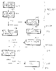
Referring to Figure 10, the four overlapped stages of the pipelined L 1 snoop
operation of
the invention are as follows: REQUEST 571, SNOOP 572, ACCESS 573 and FLUSH
574. The various registers, arrays and controls comprising these stages have
been
previously described in connection with Figures 2C, 2D and 6, and are separate
pipeline
stages from those described with respect to the load/store unit 110, Figure
2A.
During REQUEST 571, a directory access snoop request is pending to the L1
cache
directory 440. If directory address register 414 is available as determined by
DC control
470, then the snoop address will be latched into register 414 from cache
controller snoop
(CCS) address register 670 (Figure 6) on DC snoop address line 671.
EN9-96-038 28
CA 02240351 1998-06-11
During SNOOP 572, cache directory 440 is accessed and the result of the snoop
is latched
in DC control 470. At the same time, data cache read address register 408 is
latching the
address for the access stage of the snoop pipeline from line 415 for access in
the
following cycle.
During ACCESS 573, cache arrays 400 are accessed while results from the SNOOP
stage
are processed. The data read out of cache array 400 during the access stage
are latched in
register 452.
During FLUSH 574, the cache data latched in register 452 during the ACCESS
stage is
sent to L2 CCU over DC write data line 425.
When the data cache is snooped as previously described, any data transfers
resulting from
the snoop are sent to the L2 CCU. The L2 CCU in turn will transfer this data
to either the
L2 cache or system bus, depending on the originator of the snoop request. For
instance, a
snoop resulting from an ATU request will cause the data being transferred by
the snoop
operation to be placed into the L2 cache. If, on the other hand, the snoop is
resulting
from a system bus operation the data will be transferred out to the system
bus. Snoop
data from L 1 may be merged with L2 cache data so that an entire 128 bytes
corresponding to an L2 cache line size will be transferred out to the system
bus. When
placed on the system bus, the data will then either be directed to main memory
or another
processor, depending on the operation.
If multiple data transfers are required out of the L 1 cache for a given cache
line, then a
pipeline hold is sent to the REQUEST and SNOOP stages of the pipeline and the
EN9-96-038 29
CA 02240351 1998-06-11
ACCESS stage is then repeated. Thus, operation is fully pipelined when no data
transfers
occur, and at least one stall cycle is required when data transfer occurs.
Referring to Figures 8 and 9, the timings presented in accordance with this
preferred
embodiment of the invention illustrate the improved operation with respect to
that of
Figure 7. As in Figure 7, in Figures 8 and 9 the progress through cycle times
1-10
(Figure 7), 1-7 (Figure 8) and 1-5 (Figure 8) of two snoop requests,
designated by "1" and
"2", respectively, is shown through various stages 571-574. The cache busy
time
presented to the processor is reduced by three cycles and the gaps between
data transfers
from L 1 cache 400 are removed. The data transfer path from L 1 is line 453
through
multiplexer 424 to cache read line 425.
Cycle number 3 demonstrates when a pipeline hold occurs due to the need to
repeat the
ACCESS stage 573 to read another quadword (sixteen bytes) from cache 400; the
previous SNOOP stage 572 is held at its current position into the following
cycle. If no
data transfer from the first cache line was required, then no hold would occur
and the
ACCESS stage 573 would proceed to the second cache line in the following
cycle.
The embodiment of Figure 8 may be extended to a variety of L 1 and L2
configurations.
Another embodiment of the invention, for example, provides a 32 byte L1 line
size and
128 byte L2 line size. Up to four L 1 directory 440 accesses occur for every
forwarded L2
snoop in this case and the cycle savings compared to the former implementation
becomes
even greater.
The invention also allows generating hold conditions in the FLUSH stage 574 of
the
pipeline which then are used to block the REQUEST, SNOOP and ACCESS stages
571,
EN9-96-03 8 3 0
CA 02240351 1998-06-11
572, and 573, respectively, from advancing. An implementation of this
invention also
takes advantage of this mechanism to perform L 1 cache data error correction.
These hold
conditions are generated DC controls 470, in the FLUSH stage 574.
The invention is also extendable to other system organizations. In particular,
L2 cache
104 is not necessary to make this approach effective. Memory access requests
(i.e., DMA
operations) exceed L 1 cache 400 line size in certain implementations and can
take
advantage of this invention if L 1 cache 400 snooping is necessary.
The advantages of the method of the preferred embodiments of this invention
include
reducing the number of cycles required for an L 1 snoop operation, and
avoiding delays
between first and second cache blocks which cause delays in memory access
associated
with snoops.
It will be appreciated that, although specific embodiments of the invention
have been
described herein for purposes of illustration, various modifications may be
made without
departing from the spirit and scope of the invention.
EN9-96-03 8 31