Note: Descriptions are shown in the official language in which they were submitted.
CA 02240630 1998-06-15
WO 97/23032 PCT/SE96101661
1
DIGITAL CALIBRATION OF A TRANSCEIVER
The present invention is directed generally to
radiocommunication systems and, more particularly, to
techniques and structures for calibrating transceivers
used in radiocommunication systems.
The first cellular mobile radio systems in public use
were analog systems used to convey speech or other analog
information. These systems comprised multiple radio
channels for transmitting analog information between base
and mobile stations by transmitting analog-modulated radio
signals. More recently, digital systems have been
implemented due to, for example, their promise of
increased system capacity premised on their greater
ability to tolerate interference. For example, in a time
division multiple access (TDMA) radiocommunication system,
each frequency can support a plurality of time-multiplexed
channels, while in code division multiple access (CDMA)
signals are encoded to such a degree that a high level of
self interference is tolerable. Due to large existing
customer bases having analog-only terminal equipment,
dual-mode systems which support both analog and digital
channels are becoming increasingly popular in certain
areas. In the U.S., for example, systems specified by the
EIA/TIA IS-548 publication are dual-mode systems.
In an analogous manner, digital signal processing
(DSP) has become more prevalent in the radiocommunication
industry. for a variety of reasons. For example, unlike
' analog circuits, the operation of digital circuits does
not depend on precise values of the digital signals. That
is, since binary zeros and ones can be represented by
significantly different voltages, the precision at which
such voltages are held need not be very great. As a
result a digital circuit is much less sensitive to the
CA 02240630 1998-06-15
WO 97/23032 PCT/SE96/01661
2
tolerances of component values and is also fairly ,
independent of temperature, aging and other external
parameters. The accuracy of digital circuits is thus much ,
more reliable.
One part of the radiocommunication industry where the
prevalence of DSP is having a significant impact is the
design of radio transceivers. A transceiver, which is a
combined transmitter and receiver, is used for
transmitting and receiving signals over an air interface,
e.g., between a base station and mobile station in a
cellular system. Although the signals being transmitted
and received are analog signals, the modulation may be of
either analog or digital type, and the information carried
by the signal will be digitally processed. Thus, a
transceiver that uses digital signal processing techniques
in a radiocommunication system is denoted a digital
transceiver in this specification, although it may still
contain analog parts, such as amplifiers and filters (and
sometimes synthesizers and mixers), and regardless of
whether the radio signals to be processed by the
transceiver use analog or digital modulation.
In Figure 1 a conventional digital transceiver 10 is
shown schematically. Therein, a receive antenna 12 is
used to capture signals transmitted over the air interface
from, for example, other base stations and mobile stations
(not shown). The received signals are input to analog
receiver 14. Analog receiver 14 can include, for example,,
receive filters, downconverters and amplifiers for
processing the signals received via antenna 12. However,
many functions associated with processing received signals
may not be included in block 14 as these functions are now
performed using digital signal processing as described '
below. Accordingly, after being processed by the analog
components of receiver 14, the output signal is provided
to A/D converter 16 which transforms the analog signal
CA 02240630 1998-06-15
WO 97/23032 PCT/SE96/01661
3
, into a digital signal. This allows digital computing part
17 to operate on the received signal and complete the
. signal processing which was not performed by analog
receiver 14. For example, digital computing part 17 can
be used to perform demodulation and decoding of the
received signal.
On the transmitter side, digital computing part 17
performs various DSP routines which are used to prepare a
signal for transmission, e.g., encoding and modulation.
The digital signal output from digital computing part 17
is then input to a D/A converter 18 which transforms the
digital signal into an analog signal. This analog signal
is then received by analog transmitter 19 which includes
various analog components that complete the signal
processing for transmission by, for example, filtering,
frequency upconverting and amplifying the signal before it
is coupled to transmitting antenna 20.
Despite the fact that the number of analog components
used in digital transceiver 10 have been reduced (i.e., by
the substitution of DSP routines which perform signal
processing tasks previously performed by additional analog
components), the remaining analog parts (i.e., those
denoted by blocks 14 and 19 in Figure 1) continue to
suffer from the imperfections described above. These
imperfections result in gain and offset errors being
introduced into the signals which are output from blocks
14 and 19.
To exemplify how such errors are introduced and how
they are compensated according to a conventional solution,
a model of an analog receiver will be studied in more
detail. Those skilled in the art will appreciate that
signals described herein are typically mathematically
complex, i.e., with real and imaginary components.
Accordingly, complex mathematics (e. g., complex-
conjugation) is typically used to describe operations on
CA 02240630 1998-06-15
WO 97/23032 PCT/SE96/01661
4
these signals. However, to simplify this description the
complex, nature of signal operations is not shown
explicitly in the equations and figures presented herein. ,
As mentioned above, an analog receiver normally
suffers from a number of imperfections. Some of these
imperfections create signal errors, such as gain errors
and of f set errors , that can be introduced to the wanted
signal. Figure 2 models how an analog receiver introduces
an offset error and a gain error to a wanted signal Sw..
Therein, received signals are again captured by antenna
12. In the model of Figure 2, ideal processing performed
by receiver 14 is represented by block 22 which outputs
the wanted signal SW, i.e., block 22 represents the effects
of ideal analog components which have none of the
imperfections described above. Signal processing blocks
24 and 26 represent the total offset and gain errors
introduced onto the wanted signal SW by imperfections
associated with the analog components of receiver 14.
More specifically, block 24 represents the introduction of
offset errors to the wanted signal and block 26 represents
the effects of gain errors introduced by the analog
components. The output signal, with introduced errors, is
then represented by erroneous signal So. Thus, the
erroneous signal So output by the receiver can be expressed
as:
So (1+GaineP$) (SW+Offset~P$)
where:
SW=Wanted signal
So-=Erroneous signal
Offseteps=Amplitude of the '
composite offset error
Gain~P$=Amplitude of the composite
gain error
CA 02240630 1998-06-15
WO 97/23032 PCT/SE96/0166I
In a conventional receiver errors are typically
compensated at the stage where they arise, using
adjustment potentiometers and other adjustable analog
components. Figure 3 illustrates the principles of
5 conventional calibration. Therein, the same reference
numerals are used to denote the elements which were
previously described with respect to Figure 2. However,
Figure 3 also includes an offset compensation factor,
Offsetk, and a compensating gain factor, Gaink.
By adjusting the variable analog components to have
values Offsetk=Offseteps and Gaink=(1+GainCP,)-', the equality
So"~ SW will be achieved, whereby the receiver will be
ca 1 ibrated . The s igna 1 So"c wi 11 then be f ed through the
A/D converter 16 to the digital computing part 17 for
further processing.
As mentioned above, conventional calibration
techniques rely upon the inclusion of adjustable
components to compensate for errors introduced by analog
components' imperfections. These adjustable components
are used to realize the adjustments modelled by Offsets and
Gaink. A more specific example of conventional calibration
which illustrates this usage of adjustable components will
now be described in terms of a transmitter portion of a
digital transceiver. One example of an analog modulator
for modulating analog data onto a carrier is the
conventional quadrature modulator illustrated in the block
diagram of Figure 4. Quadrature modulators take advantage
of the quadrature phases of sine and cosine waves to
modulate twice the information on the radio carrier wave.
For example, the even bits in a digital information
datastream can be modulated on the cosine wave, and the
odd bits in the digital information datastream can be
modulated onto the sine wave.
In Figure 4, the analog quadrature modulator includes
an "in-phase" or I modulator 40, a "quadrature" or Q
CA 02240630 1998-06-15
WO 9?/23032 PCT/SE96/01661
6
modulator 41, and a phase-splitting network 42 for
supplying cosine and sine carrier frequency signals,
respectively. Ideally, the signals provided by the
network 42 are cos(c,~t) and sin(c~t) , where co is the carrier
signal's angular frequency. Also shown in Figure 4 are an
I and Q modulation generator 43 for supplying I and Q
modulation signals, a combination network 44 for adding
the outputs of the I modulator 40 and the Q modulator 41,
and trim potentiometers 45, 46 for carrier balance/d.c.
offset adjustments for the I and Q signals, respectively.
Additional trim potentiometers 47, 48 for amplitude
matching the I and Q signals, respectively, are also shown
in Figure 4. The phase-splitting network 42 may also be
adjustable, as indicated by the diagonal arrow, to achieve
as nearly as possible the desired 90° phase difference
between the sine and cosine carrier frequency signals.
The block diagram of Figure 4 shows one exemplary way
in which adjustable, analog components have been used to
conventionally calibrate an analog device. However, these
types of conventional calibration techniques rely upon the
adjustment of potentiometers, capacitors and inductors
during manufacturing. As will be recognized by those
skilled in the art, this calibration process is both
costly and unreliable. Moreover, there are certain types
of errors which cannot be easily compensated for using
these conventional techniques, e.g., in-band filter
ripple. In-band filter ripple refers to the variation in
the sensitivity of a receiver when tuning to different
frequencies or channels within the transceiver's frequency
range. This ripple is caused by the presence of band- '
limiting filters which are used in the receiver to remove
strong, out-of-band signals. Unfortunately, in-band '
ripple can lead to a variety of difficulties, including
inaccurate signal strength measurements.
CA 02240630 1998-06-15
WO 97/23032 PCT/SE96/01661
7
SUMMARY
These and other drawbacks and limitations of
conventional methods and systems for calibrating
transceivers are overcome according to the present
invention. According to exemplary embodiments of the
present invention, errors introduced by the analog
components in the digital transceiver, i.e., in the analog
receiver portion and in the analog transmitter portion,
are compensated in a digital computing part. That is,
during the processing of signals which are received (or
are to be transmitted) by digital signal processing
routines, compensating coefficients can be inserted into
the calculations to offset the errors that have been or
will be introduced by the analog components of the digital
25 transceiver.
According to one aspect of the present invention,
ranges of the A/D and D/A converters used in a digital
transceiver are selected so that errors are properly
transferred between the analog and digital sections. This
allows the digital compensation to be provided accurately.
According to another aspect of the present invention,
various techniques are described for determining the
calibration values which will be used to adjust signal
values to compensate for errors introduced by analog
components. These calibration values can then be stored
in a memory in the transceiver and retrieved for usage in
digital signal processing routines.
BRIEF DESCRIPTION OF THE DRAWINGS
The foregoing, and other, objects, features and
advantages of the present invention will be more readily
understood upon reading the following detailed description
in conjunction with the drawings in which:
CA 02240630 1998-06-15
WO 97/23032 PCT/SE96/01661
8
Figure 1 is a block diagram generally illustrating -
portions of a conventional digital transceiver;
Figure 2 is a block diagram modelling errors
introduced by an analog receiver;
Figure 3 is a block diagram modelling conventional
calibration techniques for the analog receiver of Figure
2;
Figure 4 is a schematic illustrating conventional
calibration of an analog transmitter using adjustable
components;
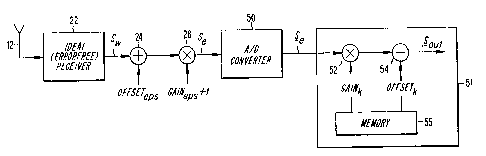
Figure 5 is a block diagram modelling calibration in
a receiver according to an exemplary embodiment of the
present invention;
Figure 6 is a block diagram modelling calibration in
a transmitter according to an exemplary embodiment of the
present invention;
Figure 7 is a block diagram illustrating a digital
signal processing function in which calibration techniques
according to the present invention can be implemented;
Figure 8(a) is a flowchart illustrating an exemplary
method for calibrating a transceiver according to the
present invention;
Figure 8(b) is another flowchart illustrating another
exemplary method for calibrating a transceiver according
to the present invention; and
Figure 9 is a graph illustrating in-band filter
ripple and techniques according to the present invention
for compensating same.
DETAILED DESCRIPTION
Those skilled in the art will appreciate that the
inventive concepts disclosed herein relating to
compensating for errors introduced by analog radio
components in a digital computing part are reciprocal in
the sense that they are applicable both to the receiver
CA 02240630 1998-06-15
WO 97/23032 PCT/SE96101661
9
portion and to the transmitter portion of a digital
transceiver. Accordingly, although various portions of
the text below provide different examples in the context
of the receiver portion and of the transmitter portion
individually, it should be understood that the teachings
of each example can also be applied to the other portion
not explicitly described therein.
According to an exemplary embodiment of the present
invention, in a receiver portion of the transceiver the
uncalibrated signal is fed through the A/D converter,
whereupon errors introduced by the analog receiver are
compensated for by the digital computing part. Figure 5
illustrates this concept by way of a block diagram.
In Figure 5, the notation So", denotes the digital
representation of the analog signal So"~. Like the
foregoing figures, Figure 5 includes several elements
which have been described above, the description of which
is not repeated here. A/D converter 50 provides an
uncalibrated digital signal S~ which is provided to digital
computing part 51. A/D converter 50 may differ in range
from A/D converter 16 for reasons described below. In
digital computing part 51, compensating factors are
applied to the uncalibrated signal S~. Specifically, a
compensating gain factor, Gaink, and a compensating offset
factor, Offsetk, are applied to the uncalibrated signal at
blocks 52 and 54, respectively. These values can be
retrieved from a memory device 55, e.g., a non-volatile,
flash memory. Thus, the digital output signal S-0ut can be
calculated from So"~ (SN.+Offsetepg) (1+Gaine,Ps) (Gaink)-Offsetk.
By setting the values of Offsetk and Gain, so that
Offsetk=Offset~ps and Gaink=(1+Gain~Ps) '. S~"t 5,~. will
be
achieved, whereby the receiver portion of the digital
transceiver will be calibrated. Exemplary calibration
techniques for determining, storing and retrieving
CA 02240630 1998-06-15
WO 97/23032 PCT/SE96/01661
appropriate values of Offsetk and Gaink which will maintain
these equalities are described below.
Notice that between introduction of the errors at ,
blocks 24, 26 and compensation of the errors at blocks 52,
5 54, there takes place the intermediate process of A/D
conversion at block 50. A/D conversion is performed by
assigning an analog signal sample to one of a plurality of
quantizing levels. For example, an 8-bit A/D converter
has 2g = 256 different quantizing levels. Since there are
10 an infinite number of actual analog amplitude values, this
conversion process introduces an error, known as a
quantizing error, which has a maximum value of ~ 1/2 the
size of a quantizing interval. This is significant in the
context of the present invention because the errors added
to the wanted signal SW will affect the quantizing error
inherent in signal S~ since compensation is performed
downstream of the A/D converter. Compare this situation
with that of the conventional solution of Figure 3. In
the conventional solution, the errors introduced by the
analog circuitry do not effect the quantizing error
introduced by conversion since the errors are compensated
for at a point upstream of the A/D converter.
Accordingly, systems designed according to the
present invention should determine an appropriate range
for A/D converter 50 taking this factor into account.
Thus, according to another aspect of the present
invention, the range of the A/D converter 50 is sized
using a model of the analog receiver with the imperfection
errors included. For example, if the errors introduced by
the analog receiver 14 are on the order of 5-25~, then the
A/D converter 50 can be selected which is 1 bit larger,
e.g., 9 bits instead of 8 bits, than the corresponding A/D '
converter 16 in a conventional system to provide a desired
level of performance. Those skilled in the art will
recognize, however, that if the errors are significantly
CA 02240630 1998-06-15
WO 97/23032 PCT/SE96/0166I
11
larger, then more,bits may be needed to characterize the
signal.
As mentioned above, this technique is reciprocal and
can also be applied to the transmitter side of digital
transceiver 10. This is illustrated by the block diagram
of Figure 6. Therein digital computing part 51 also
includes a processor 61 which generates signals for
transmission. As will be appreciated by those skilled in
the art, processor 61 can be connected to, for example, a
switching unit {not shown) which forwards information to
be transmitted over a radio channel to a base station in
which a digital transceiver according to the present
invention is located. The processor 61 performs various
digital signal processing routines on the data to be
transmitted, e.g., encoding and modulation. Then, a gain
compensation value is applied to the signal output from
processor 61 at block 62 and an offset compensation value
is applied to the signal at block 63. These compensation
values can be retrieved from memory 55. The output of
digital computing part 51 is then applied to D/A converter
64. As described previously, D/A converter 64 can be
sized according to an aspect of the present invention so
that the compensation values applied to the signal to be
transmitted in the digital computing part 51 da not create
larger quantization errors than the uncompensated signals
would have created in the conventional system of Figure 1.
Then, the analog signal is applied to the analog
transmitter portion 19 wherein the gain and offset errors
created by the analog components (e. g., the power
amplifier, filters, etc.) affect the signal to be
transmitted as modeled by block 66. Lastly, the signals
' are coupled onto transmitting antenna 20 for transmission
over an air interface.
Having described an overview of compensation
techniques according to the present invention, an
CA 02240630II2003-05-23
12
exemplary implementation will now be described with respect
to Figure 7. A block diagram of an exemplary system for
performing frequency modulation of a signal by first
separating the signal into its I and Q components is depicted
in Figure 7. In the figure, an incoming digital signal
sample stream is provided to a node 73 which sends the
samples to cosine and sine component generators 74 and 75.
Cosine and sine generators 74 and 75 can, for example, be
implemented as DSP routines which access look-up tables (not
l0 shown). For readers interested in more details of exemplary
techniques for generating sine and cosine values, U.S. Patent
5,778,027 which issued July 7, 1998 and entitled "Method and
Apparatus for Determining Signal Components using Digital
Signal Processing" to Thomas Ostman et al. can be consulted.
The cosine and sine component information is then provided to
digital-to-analog (D/A) converters 76 and 77, respectively,
for conversion of the component values into corresponding
analog signals. The analog signals are then modulated onto a
carrier in modulator 78, whose output is provided to a radio
part 79 for transmission.
The values stored in the look-up tables can be adjusted
based upon the values of Offset, and Gain, which have been
determined for the analog transmitter portion 19. This
compensation is indicated by the gain/offset input arrows to
cosine generator 74 and sine generator 75. In this way,
compensation can be provided in digital computing part 60 as
part of the DSP routine which performs signal modulation.
In a similar manner, compensation for errors introduced
by analog receiver portion 14 can be achieved by adjusting
sample magnitudes used to demodulate signals in a DSP routine
performed by a digital computing part 51.
CA 02240630 1998-06-15
WO 97/23032 PCT/SE96/01661
13
Those skilled in the art will, however, appreciate that
the compensation can also be performed by adjusting other
values used in calculations performed by the digital
computing part (e. g., DSP routines) of a digital
transceiver.
The digital computing part 51 can be set in a
calibration mode, whereupon the parameters Gaink and
offsetx can be determined using a calibration routine. A
first exemplary calibration routine is described in the
flowchart of Figure 8(a). For example, suppose that the
parameters are initially set such that Gaink=1 and
Offsetk=0 at step 80. Then by using the equation
Sa"t=(SW+Offset~Ps) (1+Gain~QB) and measuring So"t for two
different signals input to the transceiver, values can be
calculated for Offset~P$ and Gainep5 at steps 81 and 82,
respectively. For calibration, So"~ should be set equal to
SW, which means that Offsetk and Gaink can be set equal to
Offset~QS and Gain~Ps, respectively. The calibration values
thus computed are stored in memory 55 in the digital
computing part 51 of the digital transceiver at step 83.
Note that the initial values of Offsetk and Gaink used
in this description were chosen to simplify the
explanation of an exemplary calibration routine. In an
actual implementation other initial values may be chosen.
For example, initial values for Offsetk and Gaink can be
set to typical values associated with the type of receiver
used. When the receiver is operating in a non-calibration
mode, the calibrated values of Offsetk and Gaink can then
be retrieved from the memory 55 to achieve equality
between Soul and SW. This retrieval can, for example, be
s
performed at initialization of the transceiver.
The flowchart of Figure 8(b} depicts another
exemplary technique for calibrating an analog portion of
a digital transceiver. In particular, offset and gain
CA 022406310 2003-05-23
14
errors can be compensated by performing the steps illustrated
in Figure 8(b). First, at step 84, a signal transmitted at a
particular channel frequency can be input to the receiver at
each of a plurality n of different signal strengths indexed
i = 1 . . .n. Then, the output of the A/D converter for each
of the different signal strengths can be used to determine a
nominal gain value and a nominal offset value as denoted by
step 85. These values can be computed using, for example,
linear regression as set forth below, where a(i) denotes the
to converter output for each input i and d(i) denotes the signal
strength of each input i.
Ea (i) d (i) - (~a (i) ) (Ed (i) )
K = n
Ea (i) 2- ( (~,a (i) ) (Ea (i) ) )
n
O = Ed (i) - KEa (k)
n n
The nominal gain value K and nominal offset value 0 can then
be converted into a compensating value at step 86 according
to the equation Scorrected=K*S+0. The use of regression
techniques in this context is well known in the art and the
interested reader is referred to "Probability and Statistics
in Engineering and Management Science" authored by Hines and
Montgomery, e.g., pages 359-366 and "The Electrical
Engineering Handbook" edited by Richard C. Dorf at pages
2511-12. This value can be used, for examples to adjust
cosine and sine values in the look-up tables (described
above) so that the I and Q components determined by the
demodulation signal processing routine
CA 02240630 1998-06-15
WO 97/23032 PCT/SE96/01661
. in digital computing part 51 are adjusted to reflect
errors introduced in the analog receiver portion 14.
Other techniques for using the nominal values K and O to
compensate for analog imperfections will be apparent to
5 those skilled in the art.
As mentioned above, certain errors may change in
value as a function of frequency. For example, according
to this embodiment, the in-band filter ripple errors
described above can be separately compensated for by
10 providing an additional offset compensation associated
with a particular channel frequency at which the
transceiver is operating. However, RSSI error
attributable to in-band filter ripple is not measured for
all channels, but only for a set of channels which will
15 enable RSSI compensation for all in-band channels
associated with a transceiver. From the measured
channels, the rest of the channels can be compensated for
using interpolation. The number of channels which are
measured in the set should be chosen so that a sufficient
accuracy is attained. In this exemplary embodiment eight
channels are selected for measurement. This can be
visualized by the graph illustrated in Figure 9. Therein,
it is desired to compensate for variations in measured
signal strength attributable to in-band filter ripple.
Absent in-band filter ripple, in-band measurements would
closely follow the line RSSI1. However, as seen in the
figure, the actual measured signal strengths vary both
above and below this line within the in-band frequencies
f1 through f2. Accordingly, eight different frequencies
are measured and the difference between the measured RSSI
and the ideal RSSI are determined. For example, at step
87 of the flow chart of Fig. 8(b), the output of the A/D
converter can again be measured, but this time at a
plurality, e.g., eight, different channel frequencies for
a single signal strength. The offset is then computed for
CA 02240630 1998-06-15
WO 97/23032 PCT/SE96/01661
16
each output of the A/D converter. Specifically, this is
performed using the following equation:
Offset(channel)=(inputsignalstrength/K)-
converteroutput(channel)
Then, the offset value for each channel is stored in the
memory 55 at step 88. This additional offset compensating
value can be used to improve the compensation described
above by CalCUlati.ng Seart~ud-Knominal*S + Onominal + Dehannel ~ ~ohunnct Can
be a value which is determined by either using the
measured offset (channel) which is closest in frequency to
the channel at which the transceiver is operating or by
interpolating the two offset (channel) values between
which the current channel falls.
The above-described exemplary embodiments are
intended to be illustrative in all respects, rather than
restrictive, of the present invention. Thus the present
invention is capable of many variations in detailed
implementation that can be derived from the description
contained herein by a person skilled in the art. All such
variations and modifications are considered to be within
the scope and spirit of the present invention as defined
by the following claims.