Note: Descriptions are shown in the official language in which they were submitted.
CA 02240633 1998-06-15
W O 97/23Q71 PCTAUS96/19653
ERROR CORRECTING TIMING REFERENCE DISTRIBUTION
BACKGROUND
The present invention relates generally to global time lefer~lce signals
S for use in teleco..~ ionc ~y~llls and more specifically for ~;. rl,..,le
syncl~u.,i,~l i,)"
Synchlo~ ation is an i~ o~ part of many tclccu....l-..~-ic~tions
systems. In order to provide system ~yllchLûni~alion, a co~ ti~ nc system needs
to di~Llil~uL~ accl~r~te fre~uency and time l._r~ ce signals. For example, in a time~0 divisionmultiple access (TDMA) mobile cU....~ ic~tions nelwol~, abase station
bursts of data known as airframes ~or simply frames), to mobile units
traveling in an area serviced by the base station. In an American Digital Cellular
(ADC) system for example, a frame is def~ed as a digital packet cont~ining SiX time
slots trancmitterl at a 25 Hertz frarne rate. This exemplary frame format, illllstr~t~rl
15 as PIG. 1, is used in the D-AMPS system specified in EIA/TL~ IS-54B. However,those skilled in the art will appreciate that other systems, such as that specified by
Global System for Mobile Co..~ ."i~;on (C;SM), may provide dirre~ L frarne/time
slot forrnats and timing.
Con~sider the situation depicted in FIG. 2. An original base station BSl
is h~mllin~ a coll.~ec~ion between mobile station MS and the network as ~ sellLed
by the Ll,1-.x...;.~,ion link TLl between base station BSl and the mobile ~wiL~ g
center MSC. The mobile station then moves to a position MS' wherein it is
~let~ d that this cvl...Pc';on is best handled by base station BS2, e.g., to ill~rov~
the signal ~uality of the c~ on. The system ;--~ s a handoff procedure by
25 S~ l7i~ a~l~l;a~ comm~n(lc to base stations BSl and BS2 over tr~ncmiCcion links
TLl and TL2. The mobile station MS may or may not be informed of the impending
handoff.
At some time a~ter ~e handoff decision is made, trancmiccions will
begin from the base station BS2 and ~ from base station BSl. In some cases,30 e.g., where a mobile station has the capability of ~,.Ç~ i~ diversity combination or
selection of plural signals, it may be desirable to allow tr~ncmi~cion to continue from
CA 02240633 1998-06-15
W O 97/23071 PCTAUS96/19653
--2--
both base st~tiQn~c for some time period. In other cases, it may be desirable to have
little or no overlap in the Lla~x,llicsionc from base st~tio~C BSl and BS2. In either
scenario, it is important to ensure that no frames are lost during the handoff
procedure. Thus, it is desirable that the mobile station cleanly receive a last frame
5 from original base station BS1 followed by a first frame from base station BS2. This
involves at least two timing aspects: (1) estim~ting the dirr~ ce in propagation delay
bc;~w~ell the original base station BS1 and the mobile station MS and that between the
new base station BS2 and the mobile and (2) synchl~ g the ~ iCcions b~Lw~e~
the base stations so that the frames from each base station arrive at the mobile station
10 at the desired times.
Providing such ~yllcllrolJi;~ation however is ~iffirlllt as there is very little gap
time between the tl~ frames. In order to synchlu,li~e the L~ x..~ixxion of the
frames of the two different base stations, BS1 and BS2, a highly ~rCl~r~te and guicldy
disc~"lible reference signal must be provided such that the base stations are time
15 synchronized within, for example, 2 microseconds to ensure that the frame decoder in
the mobile will not be disturbed by lost, or duplicated data.
A second application for the syncluol~.~dlion of ~ mPs in a
telecc..---..~.~ir,~tions system occurs when a single base station collLaills multiple
tr~nXceivers that are each tr~ncmittin~ the same, or subst~nti~lly the same, information
20 to a mobile unit. The Ll~scei~ can be s~araLed within the same base station or
base station site, or lla~scei~ from neighboring sites can cooperate for a call
h~n~1lP~l by a common ~wilcllill~ center, wherein the neighboring sites are globally
~yllchLu~ ed. Each ll~ceivt;l can lld~lllil at slightly ~lirre~llL frequencies in order
to avoid illl~,lL~ ce. As the base station L1A~ '; the airframes to a mobile unit, the
25 mobile unit l~,ceivt;s each of the signals and combines them such that the signals
appear much ~Llunge~. This is often referred to as simlllr,~cting. One way to achieve
a working cimnlr~cting is to ~yl~cl~o~e the airframe timing of two L~ sceiv~l~ and
then have the L~lsceiv~l~Lldl~llliL airframes with a known offset relative to each
other. However, in order to be able to combine the signals when received at the
30 mobile station, the l1A~ ;C~;O11 of signals must be synchLo~t;d by the base st~tio~s.
Forthisapplir~tion, ~y~hl~u~ ionbetween~ r~ shouldbetl~""i"P-l
CA 02240633 1998-06-15
W O 97/23071 PCTrUS96/19653
--3--
within, for example, ten microseconds. In order to srllclllol~i~ the airfr~m~s,
~ifrr~me data clocks and syncl~ aLion signals are phase locked using a l~fe~ ce
distribution signal.
~ In any co,....... ~ ;ons system, accurate ~ LIilJuLion of frequency and time
5 l~f~ l~e~e signais is complicated and expensive. The dislli~uLion of timing lcfcl~ llce
signals is also a continuous source of errors that can be Tiffi- llt to d~ . To
provide ~yncl~o~ ;oI in a co"".,....i~ ~t~ons system, a phase-locked loop (PLL) can
be used to lock to a l~f~ ce fre~uency. For P~mrle, a ~pical analog PLL may
include a phase co...p--,.tor, a low-pass filter and a voltage controlled oscillator
10 (VCO). Accorlillg to this allallgellle~ the output of the VCO is fed back as one of
the inputs to the phase conl~a~Lor and, tvpically, a low frequency lcr~lcllce signal
co"~i~L;"g of individual ~yllchlul~i~LiOn pulses is fed into another input of the phase
c~ . .tor. As a result of this cor~lguration, the receiver will be very susceptible to
errors picked up in the timing ~ere.~nce signal distribution ,~ T;,...~ For example, in
con-v~ ;o.~ y~ s, when spurious frequency deviations of the ~ e.lce signal
cause errors, these errors are propagated through the fee~lh~ r loop. This in n~rn may
move the VCO out of its specified operating frequency range, reslllting in a
breakdown of c~ ti~nS. In addition, these errors can also add to the initial
time required to obtain locked c~n Tition This in turn pr~ Yc~ conventional systems
from obtair~ing the synchl~ul~-~dLion accuracy needed for the applications described
above. U~O1LU~l~1Y ~tectiQn and correction of spurious or deviating timing pulses
is very rliffllJllt in these collvel~l;on~l systems.
It is t~c.~ fole an object of this invention to di~LIil UL~ a timing reference
signal that is less se,~ilivl; to errors and which will minimi7:~ the propagation of
2~ errors.
Another object is to enable the LLdllsceive~ to obtain a phase-locked
state with respect to the reference signal .~i~"irir~"lly faster than is ~lcscnlly possible
with conven~io~l systems and that will ~ a lock even if spurious errors or
i- ltlr~,cllce are introduced in the l~r~ ce signal.
It is a further object to make fault iclentifi~tion of the distributed
le~lcnce sigDal easier, so that the ~crer~nce receiver will obtain ~c~ e alarms
-
CA 02240633 1998-06-15
W O 97/23071 PCTrUS9C/19653
co,.~ g cable shorts, cable open circuit, and spurious .~ignAiling. In addition, it is
an object of the invention to provide a reference signal di~Lli~uLion while minimi7.ing
m~mlf~ctllring costs of the cn."..,.~"ir~l;on~ system.
S SUMM~RY
The fol~,goi-lg and other obiects are accomplished acco~lulg to
exemplary embo~ "~ s by distributing a l~,Çe,~l~ce signal that includes an encoded
digital symbol pulse train having a rate much higher than the actual frequency or
oc~;u" llce rate of a ,efc~ ce event l.,~l~sellL~d (For example a frame time zero that
occurs once every 40ms frame for a 25Hz signal). A first group or seqllen~e of
symbols is used to identify a low frequency signal event or reference event. A second
group or sequence of symbols is used to in~ , t~o continuous phase information. The
symbols used to identify the referellce event are made ~ignifir, ntly dirr~l~llL from the
phase illro,..,ation, making i~llonti~ tirJn of the reference event easier. By encoding a
known seqllenre of symbols to le~ s~lll the phase hlrollllaLion in the lcrt l~nce signal,
an increased amount of frequency hlfol.llalion can be prop~g,~te(1 as colll~ared with a
collvt:llLional single pulse. This also facilitates the ~letection and correction of
.Sign ~lling errors as the errors will break the expected symbol sequence. The system
can then identify and correct, or choose to ignore, the errors based on the effect the
errors will have on system pclrollllallce.
BRIEF DESCR~TION OF THE DRAW~GS
The fealules and advantages of the invention will be understood by
reading the following description in c.,lljull~lion with the dldwi~s, in which:
FIG. 1 ill~ es a frame with time slots;
FIG. 2 shows an example of base station collllllul~lcdLion with a mobile,
E~IG. 3A illustrates phase relations of the timing l~Ç~ ce signal;
FIG. 3B shows the timing l~,rt;lellce signal in relation to an inr1ir,<~tt-rl
frame time zero;
FIG. 4 is a block diagram of a digital phase locked loop;
FIG. 5 is a block diagram of an exemplary symbol correlation detector;
CA 02240633 1998-06-15
W O 97/~3071 PCT~US96/19653
_5_
FIG. 6 depicts sampling and b;t error correction according to an
exemplary embo~lhllclll of the present invention;
FIG. 7 is a block t1i~2gr~m illu~al~g an exemplary embod~nent of a
symbol detecffon unit; and
S FIG. 8 is a blocl~ diagram of ~ c~;v~ cabinets to which r~r~ellce
signals according to the present invention can be distributed
DETAILED DESCRIPTION
The various fealul,,s of the invention will now be described with
10 respect to the figures, in which like parts are itl~rltifie~l with the same r~r;;rellce
ch~r~rt~r.~
~VnE REFERENCE SIGNA~LS
The distribuffon of accurate frequency and time lefel~llce signals in
1~ telecr,~ .;c~tion~ systems can be complicated and e~el~ive. Reference signal
disL~ ion is a source of continuous e~ors that are tlifflrl~lt to detect and locate.
Errors can also lead to severe degradation of system ~clro~ ance. The technique and
l~.t~-l;l"ll used to t1i~trih~lte a ler~ ce signal, e.g., as ll~icrow~ve~ radio, or cable,
introduce spurious pulses or errors in the signal which, if Tm-letect~l can slow or
20 inhibit system operation. For example, when a collvel~lional reÇclc"ce signal is
received in a phase locked loop (PLL), the error in the l~,Ç~cnce signal is added to
the fee~lb~k loop, causing the system to take much longer to acquire a locked
frequency. As a result, the PLL could be forced outside the m~2~imnm specified error
from the ideal l.,r~c.lce Ll~ ue~y for the system.
2~ The problem with collvelllional ler~l~llce signals is that it is extremely
~iffir,nh to ~te....i-~ if errors or ullw~ ed illLclÇ~le~ce have been added to the
rcr~,.c.2ce signal. It is equally difficult to remove any errors that have been introduced
in the l~r~le~lce signal.
According to one aspect of the present invention, a time ~-m~in
30 discrete l.,r~.ence signal is ~ ;b~rd and encoded with ihlro,..~ on to enable the
system to d~l-,....;.-~ if the l~,rcl~ ce signal has enough ~c~ y. The r~,r~rcllce signal
CA 02240633 1998-06-lS
WO 97~3071 PCTAJS96/19653
in~hldes prede~ d groups or seq~len~es of symbols. By mo~ ulhlg the lcfer~nce
signal the system can d~ if each received sequence of symbols is correct for
the actual frequency mea~ .llenL. If the seq~lenre is not correct, the system can then
~1r~ if the signal should be disle~-led. The system can thus exclude a very
small part of the rercl~ ce signal that collL~ills an error. Th~.~ruLe, a much higher
level of di~Lu~ballce or noise is needed to break a lock condition. The symbols are
chosen so that, for example, spikes, cable breakage, hum, click, and static will not
appear as a good signal. The system is then able to pick system errors out of the
Lcfe.ence system errors and make corrections on single samples to make the reference
0 Sigrlal ;IlllllllI-f to small spikes and jitter that equals out on a single symbol or in an
Alt~ AIi~/e embodiment simply ignore the error. For example, errors smaller thanplus or minus 1.5 master clock (l!~CK) intervals will be filtered by sampling and
symbol ~etection units (shown in detail below) under the condition that the error will
be e(r~Aled by aIl error of the same amount in the other direction at the next transition
on the l~ ~.cl~ce signal.
The rate of symbol LIA~ ics;~m is also illl~Ol~ to the ability to
disleg~d spurious errors. As the system has to regard the period of a symbol
error(s) in C(J~ fiSOll to the mea~u,Gmel~l interval, a symbol error with a period of
1/1000 of a measu,c"lent interval will render in the reference signal an error of one
per mille or 1/1000. Thc.er(,lc, the smaller the symbol period, the higher the symbol
trAn~mi~ion rate and c~ ondingly the greater the ability to dislcg~d errors. A
cul~ ional PLL system with one pulse per refel. ~ce event will respond to a single
spike as anything between zero error up to the whole pulse interval. When using such
a convention~l n Ç~.lcc signal only a single spike per (ll~eolc.ically) eleven hours is
toler~te~l; however, when irnplemPnt~d with a PLL including a lowpass filter present
in the ~ee~b~el~ chain, about a single spike per hour can be tolerated. By using the
A~ lCÇ~l'ellCe signal for ~yllcl~u~Lion accol-li~ to the present invention, the
initial time needed to produce a locked condition will be much smaller than with a
conventional Lc~e~ ce signal. Another advantage of using a known seqllenre of
symbols is ~he ability to count errors and ~ the reliability of the lcrelcllce
signal. For the same reasons the system can also recognize errors much more quickly
CA 02240633 1998-06-15
W O 97/23071 PCTAJS96/19653
and disregard or hold the signal locked wi~in the required specification by keeping
errors from being fed back into the PLL. As a result, fewer ~ rn~n~ls are placed on
the Cil~ui~.
~ According to another embodiment of the invention, more phase
i~rù~ aLion is sent with the l~fer~ signal than is actually needed to in~ t~ a
~Çtl~nce event. In order to div~.~iry ~e i,~llnation, the phase hlrullllaLion must
behave in a way that is sufficiently different from the lcr~,Lellce event such that the
cre~cnce event is easily ~ ntifi~od The illru~ Lion is col~lised of symbols each~aving a unique bit pattern. There are basically two kinds of symbols, "phase"
symbols and "sync" symbols. The sync symbols carry both the l~rerellce event andphase illrullllation. The phase symbols only carry phase information. Symbols are
in~lic~ted by a cùntinuous flow of a unique high frequency pattern. According to one
embo-liment of the invention, the symbol pattern is one million times more unique
than the ~in~ r pulse used in a cullve,.~;on~l system. This will satisfy one parts per
million (PPM) of i"folmation c~ lr~t y simplifying the ~i~tection of any error
condition and if an error condition can be collc.;lcd.
Turning to FIG. 3A, an ~irfr~m~ timing l~Ç~lcllce (AFS) signal is
shown. The AFS signal is a composite signal culllplisillg two binary signals, AFS1
10 and AFS2 11. Accol~ to a ~leÇclled embodiment of the invention, the AFS
signal can be generated out of a 4860 kHz clock signal, CLK 12. Th~ Çole, for a 25
Hz lcre~cllce pulse, with every 48,600th tick of CLK, a violation sequence 14 isj"~lir~tl The violation seqll~nre is a sequence of sync symbols lc~,ullmg in thestream of symbols at the time of the lcr~ lce event. According to one plcf~lled
embo~lim~n~ of the invention the violation seque~e occurs at a 25 Heru rate. Theviolation sequence lasts for two cycles of the CLK 12, starting at the negative CLK
il;ol~. ~fter completion of the violation sequence, the normal sequence composedof phase symbols 1~ is resumed and will c- ntiml~ until the next violation sequence,
completing a 25 Hertz cycle.
FIG. 3A illnstr~t~s that the order of the toggle between AFSl 10 and
AFS2 11 is reYersed during the violation seq~lenre. For example, in FIG. 3A AFSl10 would normally remain low and AFS2 11 would toggle low. However, with the
CA 02240633 1998-06-15
W O 97/23071 PCTrUS96/19653
beginning of the violation mask AFS2 11 is held high and AFSl 10 toggles high. In
other words, with the begil~ing of a violation seqUPnre~ AFS2 11 will toggle when
AFSl 10 normally would have toggled, and vice versa. Through use of the chosen
encoding scheme, the AFS signal will propagate an airframe time l~çclcllce (airframe
5 timing) with high tolerance to .li~Lulbd-lces and connection errors for several reasons.
First, the frequency of symbols is very high. This makes singular errors very
in~;~nific~nt Second, there are more symbols that can be represented than actually
are used. Therefore an error will likely ge,~l~tc a symbol that is not accepted.However, even in the unlikely event the error signal mimics one of the allowable10 symbols, it will not appear in the correct or expected sequence and thus also be
i~Pnti~l~hle. In addition, if AFS1 and AFS2 toggle at the same time, an illegal
symbol will be ~e.~ rd
Frame time zero, FTZ 16, is in~ tPd by the violation sequence as
shown in FIG. 3A. The Detected AFS and FTZ can be ~1elr~ ..li.-Pd in many ways.
15 According to a ~ cd embodiment, FTZ and the Detected AFS are clele.
when all of the sync symbols have been received with no errors and in the right
sequence. If any of the sync symbols are faulty, the whole 40 ms interval is
disregarded. Using this embodiment it has been discovered that phase information is
not nPcPSs~;y for the clete~ lion. It is enough to just count the phase information
20 errors in order to de~ -P the signal 3itter, and other errors. It will be appreciated
by one skilled in the art that the signals in FIG. 3A, except for AFSl and AFS2 are
included only for illU~LlaLivc purposes of ~1r~ a l~r~ ce event and are not
part of the AFS di~Llibution concept per se. Other ~ign~lin~ scllPmes for creation of a
lc~ellce signal would suggest thPm~Plves to one skilled in the art without departing
25 from the scope and spirit of the invention.
According to a ~lcfell~d embodiment of the invention, the air~rame
timing l~,Ee.el~ce signal, AFS, can be a 1215 l~Iz, 50/50% duty-cycle 90~ two phase
s~uare-wave signal carried by the signals ~FSl and AFS2. The 25 Hz interval
airframe timing is encoded into the AFS signal by means of a phase violation as
30 ~lPfînP~ above. The coding scheme used is similar to a two-phase Miller variant or
delay morl~ tion encoding. Of course other coding schPm~s may be used in
CA 02240633 1998-06-15
PCTfUS96/19653
W O 97/23~71
_9_
accold~ce with the present invention. According to this embo-lim~nt j;tter on the
AFS signal must not exceed + 25 nanoseconds at the receiver end. Also according to
this exemplary embotlimPnt, the m~xim7lm allowed frequency error on the AFS signal
is 1 PPM measured over an integr~tion time of 25 milli~econds, or longer. These
5 va~ues have been chosen because they do not limit design of a system and are loose
when compared with actual system ~lÇ~. ,..A~ e. A path delay introduced by
distril~uting the AFS signal from the timing master and to any airframe time lcrele~ce
Lc~ ie~ is allowed to be between 0 - 450 nanoseconds. Also according to the
~l~r~ ,1 embo~lim~nt of the invention a Master Clock of 19.44 MHz is used. As
in~ te~ in FIG 3B, one AFS .~ .. transition interval TM 17 4.86 MHz, which
is approxim~ly 206 nanoseconds; TC equals 4.86 M~z divided by 4 = 1215 kH~,
or a~L~ru~ ly 823 nanoseconds.
SYMBOL DETECTION AND CORRELATION
The airframe timing is ~lesellL~d on the incoming time re~erence signal,
AFS, as a train of symbols, see, e.g., FIGS. 3A and 3B. Each symbol lc~les~llL~ a
specific time in the ~irfr~m~. As previously mentioned, the time l~re~e.lce signal is
diversi~led into AFS1 and AFS2. Each of the two signals carries a part of the
composite AFS signal. In order to simplify the following description, the two signals,
AFS1 and AFS~, will be commonly referred to as APS, and where they differ, this
will be noted.
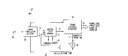
In order to geneldLe the ~irfr~mP timing signals 52, see, e.g.,
FRAMESYNC, SAMPLERATE, FRAME_TX, and FRAME_RX in PIG. 4, they
may ~e ~y~ ni~ed to a timing r~L.e.~ce signal. Once an AFS signal is ~el~ dL;;d
the signal can be ~1PCO~PC1 by the l~ceivillg unit (see, e.g., FIG. 8), for ;~ re a
sce;~ in the base station. The l~ceivi~g unit identifies and correlates the phase
~ull~aLion and the l~re~ ce event i~o~ "~tion or SYNC inform~ion According to
ano~e~ aspect of the present i~v~nLioll this can be accomplished through the use of a
symbol correlation detector ~SCD).
The SCD detects ailîld~e timing on the AFS signal by mt~ the
time belw~en the current tr~ncition on ~e incoming reference and ~e last transition
CA 02240633 1998-06-15
W O 97/23071 PCTMS96/19653
-10-
on AFSl and AFS2, respectively. It also mcasules the current signal level and
detects tr~n~itinn~ on the AFSl and AFS2. FIG. S is an example of an SCD 30
according to an exemplary embodiment of the invention. The AFS signal 20 and
master cloclc (MCK) 25 are fed into a sampling and bit error ccll~,cLioll unit 34.
5 After the AFS signal is sampled and co~le~ d~ it is output as a ~letçcte~l AFS(DET AFS) signal 37. The DET_AFS 37 is then input into a symbol ~1etloction unit36 to identify the symbols in the AFS signal to ~ie~ ...;.~P the encoded lcÇ.,,,_..ce event
i-lrol~lation and phase il~lll~dlion which is ou~uLl~d as signals AFS_TRANS 39 and
SYMBOL ID 33. These signals are then input into the Fr~mPtimP Detection Unit 38
10 along with the rietPC~(l AFS signal 37 in order to identify any symbol error, OVe11Uj~,
and the detected frame time 31, 32 and 35, respectively.
SAMPLING AND BIT ERROR CORRECTION
One advantage of using a discrete r~ç.,lcllce signal is the ability to
1~ identify errors and deviations that can occur with distribution of the reference signal.
Turning to FIG. 6, an exemplary ilnplem~ont~ti-~n of sampling and bit error correction
ur~it 34 is depicted. The AFS signal is input into a low pass filter 41 and thenPcl to a Schmitt trigger 42. The signal is then sampled in a series of D-type
latches 43. Single bit errors are then corrected using a two out of three majority gate
20 44. The sampled and corrected signal, DET_AFS 37 is then distributed to the symbol
detector. It should be noted that this function is doubled, one for AFS1 and one for
AFS2.
SYMBOL DETECTION AND ERROR IDENTIFICATION
2~ FIG. 7 shows an ex~mrle of a symbol detecti--n unit 36 according to anembodiment of the invention. The symbol deL~c~ioll unit 36 detects tr~nCition~ on the
~etect~q~l AFS signal 37. Time between the tr~n~itinns is measured with a 5-bit
counter 55 that counts from three after it is reset by ~e AFS_TRANS asserted
cr)n-liti~ n 39. The ~letçctçd AFS signal 37 is "mid bit sa}npled" as the AFS signal is
30 ~ xI;~l;on~ry to ~e sampling MCK signal. Since the count by ~he counter 55 is, and counts the duration of a level sampled at mid bit, the cou~ should
CA 02240633 l998-06-l5
W O 97/23071 PCTAUS96/196S3
start at ~ree to co~ Pn.~ for the l~u~lcaLed bit. The counter counts up to 16 and
~ then holds until reset again. The det~ct~(l SYMBOL ID 33 equals the biIIary output
of the cuullL~l 55 divided by 4. AccordiIIg to a ~er~ d embodiment of the
invention, Symbol IDs from t~e symbol ~l~Lol are as follows: 0 = burst error; 1
S = symbol 1; 2 = symbol 2; 3 = symbol 3; and 4 = o~ ull error. Note this
function is doubled, one for AFSl and one for AFS2.
Frame time is ~l~t~ct~d by c~ ;"~ ~e states of
DET_AFS~/DET AFS2, AFS_TRANSl/AFS_TRANS2, and
SYMBOL_IDlISYMBOL_ID2. Table I depicts an example of valid symbols which
10 can be used according to the teachings of this invention:
TABLE I
DET AFS AFS_TRANS SYMBOL_ID Condition
1 2 1 2 1 2
1 1 1 0 1 2 SYNC (-1)
1 0 0 1 1 3 SYNC (0)
O O 1 0 2 1 SYNC (+l)
0 1 0 1 1 2 SYNC (+2)
O O O 1 2 1 SYNC (+3)
1 0 1 0 3 1 SYNC (+4)
1 0 1 0 2 1 Phase (0)
1 1 0 1 1 2 Phase (1)
0 1 1 0 2 1 Phase (2)
0 0 0 1 1 2 Phase (3)
X X X X 4 X OverRun
X X X X X 4 OverRun
Symbols are ~1et~cte~1 at any tr~ncition on AFS_TRANSl and
AFS_TRANS2. An exception to this, occurs with an OverRun error, which is
~etect~l every master clock interval that the sihl~tion rem~in~ OverRun error ist fl~,ge~ when there are no tran~ition on one of the two or both of the signals AFSl
and AFS2 for a Liule(,uL period. According to one p~ rell~d embodiment the timeout
period is a~ ciul~L~ly 211 llliclosecollds (4096x51.44=210698, where 4096 is an
up/down counter value, and time ~ ...,. 51.44ns=1000 divided by the master clock
or 19.M). Ihe liulc~uL is sampled with an up/down counter (not shown) that counts
CA 02240633 1998-06-15
W O 97/23071 PCT~US96/19653
OV~llu115 per MCK interval. The counter will count down to zero and stay there if
there are no OV~11.111S. The counter will count for each ovellul~ up to 8191. AnOV.,~l~lll error can occur when colll~eclion is broken, e.g., cable breakage, when no
signal is ~Ptectec~ An overrun error is flagged when this counter is greater than or
5 equal to 4096. The Over~un error thus is filtered for glitches and reported as a
SymOverRun when it averages more than 50% over an integration time of 211
microseconds. When the condition from the above Table I is SYNC(0), frame time
zero (FTZ) is ~etPct~oA Continuous inll;r~tion of molllell~y phase is given by the
phase (n) symbols. The detector keeps track of the sequence by v~ ting the
10 ~i~t~ctetl condition according to the previous condition.
Table II in~lif.~t~s an example of a series of valid condition sequences.
Note this table is exemplary and other encoding sch~m~s could be used without
departing from the scope and spirit of the invention.
TABLE II
Previous: Current:
Phase(O) =~ Phase(l)
2Q Phase(l) =~ Phase(2)
Phase(2) => Phase(3)
Phase(3) =, Phase(O)
Phase(2) =~ Sync(-l)
Sync(~ Sync(O)
2~ Sync(O) =~ Sync(l)
Sync(l) =~ Sync(2)
Sync(2) =~ Sync(3)
Sync(3) =~ Sync(4)
Sync(4) =~ Phase(l)
3~ overrun =~ Any condition
symerror =~ Any condition
A ~l~t~ct~ri condition that is out of sequence is considered as a symbol
error. For in~t~n~e, if the previous symbol was Phase(l) the eA~ccled current symbol
should be Phase(2). If not then an error is ~let~oct~l When any error condition
occurs, the ~letecte~1 frame timing is not col~sid~,d valid and a symbol error is
reported at every tr~n~iti~m on either DET AFSl or DET_AFS2. Con-liti-n~ of
CA 02240633 1998-06-15
W O 97~3071 PCT~US96/19653
symbol error, and implicitly overrun errors, too, will not affect the gen~-rated frame
timing. T~e~cfolc, the det~cte~l frame timing can be updated frequently. The system
can also count the number of errors to del~ F if the signal has become unlocked.The system can ~hen decide if it should adjust the loop back time in the phase locked
S loop or if the system can go Lcl~Olalily unsynced if the error is spurious.
PREQUENCY GENERATOR AND CORRELATOR
One app~ ti~)n of the timing reference signal is to provide ai,fidn~e
s,yl~cl~o~ alion bclwcell base stations and between local Llal~scei~ at the same base
10 station as illu~Llaled in FIG. 8. According to this embodiment a time reference signal
EXT_AFS 72 is gel~ldted by a timing master TIM (not shown). The EXT_AFS is
then di~LlilJIllcd between the (lanscei~l cabinets 70. The EXT_AFS is then
distributed intern~lly to each LLd-~cei~er 80 as signal AFS 82. Each Ll~sceivtl 80
then locks its ~irfr~me tirning to this time ~f~ ce signal.
The ~y~lc~ on can be accomplished through use of a Frequency
~en~ldlc,r and Correlator (FGC) or discrete phase locked loop as shown by FIG. 4.
Each Lla~Lsceivcl 80 is provided with an FGC. In order to syncllLoll.~e the
icsi~nS of the ailrldn~es from each of the base stations and from multiple
sc~iv.,Ls within a base station, a timing reference signal (AFS) 20 is provided.20 The FGC ge,~,dtt ~irfr~m~ timing signals using the MCK 25. In order to m~int~in
synchro,Pi~dlion to AFS signal 20, the FGC adds or removes a small time ~ at
regular intervals to the airframe timing signals 52.
In an ideal ~iluaLiOIl of no time skew between the gen.,lalcd timing and
the AFS reference signal, the FGC g~ rs its ouh2ut signals di~ecLly out of the
25 MCK. When a time skew beLwee" the g~ ;cl timing and the rerclcl,ce AFS signalis present, the FGC will adiust timing by adding or removing a ~ " of time to orfrom the g~ a--rl~,e timing signals. This time qu~nh]m is ~ c....;~ by the
Timing Synthesis Se4uencer and is proportional to the MCK.
By regularly ~kcwillg the ge~ d timing signals in the FGC, the
30 signals become phase locked to the AFS signal. A complete description of the FGC
and its operation is given in co-pending U.S. Application No. 08/
CA 02240633 1998-06-15
W O 97/23071 . PCTAUS96/19653
Attorney Docket No. 027555~2, titled "Discrete Phased Locked Loop" by Johan
Jansson, filed on the same date and incol~oldL~d herein by ,~,fel_,lce.
The present invention has been ~lesrrihe~ by way of example, and
mo-lifir~ti~n~ and variations of the exemplary embo~ will suggest th~m~elves to
5 sldlled artisans in this field willluuL de~ from the spirit of the invention. The
prt;r~,led embo~ Y are merely ill~ ;ve and should not be considered l~i,LIicLivein any way. The scope of the illv~lllioll is to be measured by the appended claims,
rather than the prece~ing description, and all variations and equivalents which fall
within the range of the claims are inte~ to be embraced therein.