Note: Descriptions are shown in the official language in which they were submitted.
CA 02240653 2001-07-26
68432-329
DUAL OPERATIONAL AND BRAKE LIGHT
CONTROL FOR TRAILERS
Background of the Invention
The present invention relates to electronic adaptor
~~ circuits which convert combined stop and turn signal lights of
a trailer to operate in response to the independent stop and
turn signal lights on a towing vehicle. Such devices are well
known. Examples of trailer light adaptors are disclosed in
U.S. Patent Nos. 4,005,:313; 4,057,310; 4,270,115; 4,405,190;
4,718,853; 4,842,524 anc3 4,939,503. Some of these patents
disclose a circuit for <~dapting a three lamp system of a towing
vehicle to a two lamp system of the trailer. Other patents
such as U.S. Patent Nos. 3,849,664; 3,883,845; 3,970,860;
4,006,453; 4,064,413; 4,.325,052; 4,751,431; 5,030,938;
5,212,469 and 5,701,116 disclose trailer light converter
systems having certain advantages. For example, U.S. Patent
4,006,453 discloses a converter circuit which adapts a two lamp
trailer signal light sy~~tem to a three lamp towing vehicle
system. In this device and others the power to drive the
trailer signal lights i~> provided by the towing vehicle stop
and turn signal lights which also serve as ground for the logic
circuit. Such a design requires a complex diode isolation
network. However, if the towing vehicle lights are missing or
defective the logic of the converter will be defeated.
Furthermore, the requisite diode isolation network in
combination with output transistors, significantly reduce the
power output to the trailer signal lights. In addition, many
current vehicle lighting circuits employ sensors to detect
defective signal lights. Connecting such signal lights to
provide power to trailer signal lights causes a significant
drain on the towing vehicle lights which can cause disruption
of the defective lamp sensors and faulty indications.
1
CA 02240653 2001-07-26
68432-329
Summary of the Invention
The primary object of the present invention is to
provide a battery powered adaptor which enables a trailer
having combined stop and turn signal light systems to be towed
~~ behind a vehicle having independent stop and turn light
systems.
Another object of the invention is to provide a
device having means for de-activating the stop signal lamp on
one side of the trailer when the turn signal on that side is
being operated:
A further objE=_ct of the invention is to provide power
to the trailer lights d_i-rectly from a 12.5 volt battery, thus
isolating the signal lamps of the towing vehicle from the
signal lamps of the tra_uLer.
A yet further object of the invention is to eliminate
the need for a complex cLiode network and to properly operate
the trailer signal lights independent of the condition of the
towing vehicle signal li_c~hts in a simplified circuit for
enhanced reliability.
Therefore this; invention seeks to provide a device
for adapting combined brake and turn signal lights of a trailer
to independent brake and turn signal lights on an associated
towing vehicle, the towing vehicle having right and left turn
signal circuits and a stc>p signal circuit, the trailer having
right-hand and left-hand. signal lights, each of which has a
common filament for stop and turn signals, the device
comprising: first switching means connected to both the right
turn signal circuit and to the stop signal circuit of the
towing vehicle, a voltage source being connected directly to
2
CA 02240653 2001-07-26
68432-329
the first switching means independent of the turn signal
circuits; second switch.i.ng means connected to both the left
turn signal circuit and the stop signal circuit of the towing
vehicle, the voltage source being connected directly to the
second switching means independent of the turn signal circuits;
each of the first and second switching means operating as and
exclusive "or" gate to connect: the voltage source to the
associated one of the common filaments of the trailer lights
when only one, but not both, of the stop signal and the turn
signal circuits is energized; and each of said switching means
comprising a PNP transistor and an NPN .transistor connected in
series, each of said transistors also connected to both said
stop signal circuit and one of said turn signal circuits, and a
PNP output transistor connected with said transistors, said
1~ output transistor also ~~onnected to said independent voltage
source.
This invention also seeks to provide a device for
adapting combined stop <~nd turn signal lights of a trailer to
independent brake signa:L and turn signal lights on an
associated towing vehic:Le=_, the towing vehicle having right and
left turn signal circuits and a stop signal circuit, the
trailer having right-hand and left-hand signal lights, each of
which has a common filarnent for stop and turn signals, said
device comprising: a f~_rst switch configured to be connected
to both the right turn ~~ignal circuit and to the stop signal
circuit on the vehicle, and also configured to be connected to
the right-hand turn-and--stop signal light on the trailer; a
second switch configured to be connected to both the left turn
signal light and to the stop signal circuit on the vehicle, and
also configured to be connected to the left-hand turn-and-stop
signal light on the trailer; said first and second switches
configured to connect directly to a voltage source rather than
2a
CA 02240653 2001-07-26
68432-329
connecting to the voltage source through the stop signal or
turn signal lights of the towing vehicle; said first and second
switches each being operable to transmit current directly from
the voltage source to t:he respective right and left turn-and-
c stop signal lights on t:he trailer when only one of the
corresponding signal circuits on the towing vehicle is
operating; and each of aaid switches being operable, responsive
to signals from both th~~ stop signal circuit and the
corresponding turn signal circuit on the towing vehicle to
switch current from the independent voltage source alternately
on and off to the assoc:i;~ted turn-and-stop signal light of the
trailer, when both the brakes and turn signal circuits are
operating; and each of t:he switches comprising a PNP transistor
and an NPN transistor connected in series, each of the
transistors also connected to both the stop signal circuit and
one of the turn signal circuits, and a PNP output transistor
connected with the tran:~istors, the output transistor also
connected to the independent voltage source.
This invention also seeks to provide a device for
adapting combined stop rind turn signal lights of a trailer to
independent brake signal. and turn signal lights on an
associated towing vehicle, the towing vehicle having right and
left turn signal circuit:; and a stop signal circuit, the
trailer having right-hared and left-hand signal lights, each of
which has a common filament for stop and turn signals, said
device comprising: a first switch configured to be connected
to the right turn and stop signal circuits of the towing
vehicle and to a voltage source and further configured to
transmit current directly from the voltage source to the right
turn and stop signal circuits of the trailer without drawing
that current through the right turn and stop signal circuits of
the towing vehicle; a second switch configured to be connected
to both the left turn ar.:d stop signal circuits of the towing
2b
CA 02240653 2001-07-26
68432-329
vehicle and to a voltage source and further configured to
transmit current directly from the voltage source to the left
turn and stop signal circuits of the trailer without drawing
that current through the left turn and stop signal circuits of
the towing vehicle; each of the first and second switches
operating as an exclusive "or" gate to connect the voltage
source to the associated one of the common filaments of the
trailer lights when only one, but not both of the stop signal
and the turn signal cir~Juits is energized; and each of the
switches comprising a PNP transistor and an NPN transistor
connected in.series, each of the transistors also connected to
both the stop signal circuit and one of the turn signal
circuits, and a PNP output transistor also connected with the
transistors, the output transistor also connected to the
independent voltage source.
This invention also seeks to provide an electrical
circuit adaptor for use between a towing vehicle lighting
system having independent brake and turn signal lamps and a
trailer lighting system having combined brake and turn signal
lamps, the circuit adapt:or comprising: first and second
vehicle signal inputs configured to receive respective
electrical signals from the towing vehicle lighting system
each signal representing the state of a particular towing
vehicle lamp; a power supply input connected to a power source
for receiving a power input signal; a first transistor having a
first terminal coupled to the first and second signal inputs, a
second terminal coupled t:o the power supply input, and a third
terminal; a second tran~.i.stor having a first terminal coupled
to the first and second signal inputs, a second terminal, and a
third terminal coupled to ground; a third transistor having a
first terminal, a second. terminal coupled to the power supply
input, and a third terminal; and a trailer signal output
coupled to the third terminal of the third transistor and
2c
CA 02240653 2001-07-26
68432-329
configured to transmit a power signal from the circuit adaptor
to the trailer lighting system; wherein the third terminal of
the first transistor is coupled to the second terminal of the
second transistor forming a series connection, the series
connection being coupled to the first terminal of the third
transistor such that the signal output is coupled to the power
supply input only when one of the first and second signal
inputs are high, but not both.
These and other objects and advantages of the
1C~ invention will become apparent to those skilled in the art from
the following detailed description of the invention with
reference to the attached drawing.
Brief Description of the Drawings
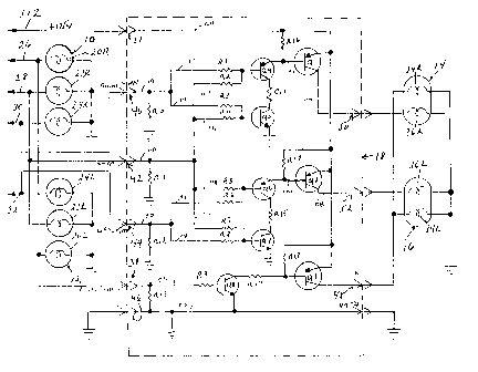
Fig. 1 is an electric schematic diagram of the
1~ preferred embodiment of the adaptor of the present invention.
Description. of the Preferred Embodiment
In the embodiment of the invention shown in Fig. l,
reference numeral 10 designates the group of right-hand signal
lights for the towing vE=_hicle, while reference numeral 12
20 designates the left-hand signal lights. Reference numeral 112
designates the voltage ;source such as a 12.5 volt towing
vehicle battery. The right-hand signal
2d
CA 02240653 1998-09-16
light of the trailer is shown at 14, and the left-hand signal light
of the trailer is designated by the numeral 16. Reference numeral
I8 designates, in its entirety, the adaptor device of the present
invention, which enables the lights of the trailer to be actuated
in a legal manner by the brake signal and turn signal circuits of
the towing vehicle, as will be described hereinafter.
The signal lights of the towing vehicle consist of two groups
10, 12 of three each with each group being arranged on the opposite
sides of the towing vehicle at the rear end thereof. Lights 20R
and 20L are the taillights (or clearance lights) on the right-hand
and left-hand sides of the towing vehicle, respectively. Lights
22R and 22L are the brake or stop signal lights on. the right and
left sides of the towing vehicle, respectively. Lights 24R and 24L
are the right turn and left turn signal lights, respectively, of
the towing vehicle. The clearance lights 20R and 20L are connected
to the light circuit 26 of the towing vehicle which causes the
lights to go on when the headlights are activated. Stop signal
lights 22R and 22L are connected to a brake or stop signal light
circuit 28, and both of these lights go on simultaneously when the
brakes are actuated. Right turn signal light 24R is connected to
right turn signal circuit 30, and left turn signal light 24L is
connected to left turn signal circuit 32, so that the appropriate
signal light is caused to flash when the turn signal lever is
actuated.
The system shown in. the drawing wherein the right-hand and
left-hand signal lights 10 and 12 each have three separate lamps or
three separate filaments, each of which has a separate function.
Most trailers have the stop and turn signals applied to a common
filament of a combination signal light. Thus, most trailers have
only two separate lamps, as generally indicated at 14 and 16 in the
drawing. These two systems are electrically incompatible, and some
modification of the systems) must occur if the lighting systems
3
CA 02240653 1998-09-16
are to be operated in a legal manner. This is accomplished in the
present invention by the adaptor device I8 which creates a stop
signal inhibiting action in the signaling circuit which is normally
provided in the electrical system of a towing vehicle having
independent stop and turn functions.
In the trailer lights 14 and 16 there are two lamps arranged
on opposite sides of the trailer, each of which has two filaments.
Filaments 34R and 34L are the clearance light filaments, which
light up simultaneously when the towing vehicle headlights are
switched on. Filament 36R is a common stop and right turn signal
for the right-hand light 14, while filament 36L is the common stop
and left turn signal for the left-hand light 16.
The adaptor device 18 preferably is housed in a weatherproof
enclosure and has six input connections 37, 38, 40, 42, 44 and 46,
each of which is a direct electrical connection to corresponding
circuits on the towing vehicle. Output connections 48, 50 and 52
are provided which permit connection to the signal lights 14, 16 of
the trailer.
Input connection 37 is connected directly to the voltage
source 112, which is 12.5 volt battery of the towing vehicle.
Input connector 46 is connected to the towing vehicle ground.
Input connection 40 is connected to the right turn signal circuit
30. Input connection 42 is connected to the stop signal light
circuit 28. Input connector 44 is connected to the left turn
signal circuit. 32, and input connection 38 is connected to the
clearance light circuit 26.
Output connection 48 provides for connection to the clearance
light filaments 34R, 34L of the trailer signal lamp 14, 16,
respectively. Output connection 50 is connected to the common
brake/turn signal filament 36R of the trailer signal light 14.
Output connection 52 is connected to the common brake/turn signal
4
CA 02240653 2001-07-26
68432-329
filament 36L of the trailer signal light. Output connection 49
provides a connection to the trailer ground.
Electrical line 54 within the adaptor device circuit 18
connects the input connection 38 to both ground via resistor R13
between line 54 and line 55 and to the base of an NPN transistor Q8
through resistor R9. The emitter of transistor Q8 is connected to
ground via line 55. The' collector of transistor Q8 is connected
through resistor R19 to the base of a PNP output transistor Q3
whose emitter is connected to the 12.5 volt input connection 37 via
i0 line 64. Resistor R18 is connected between the base and emitter of
outgut transistor Q3.~ The collector_of output transistor Q3- is
connected via line 68 to output connection 48, and~in turn to~the
light filaments 34R and 34L of trailer signal lamps 14 and 16,
respectively.
Line 70 connects to input connection 40, which goes to the
right turn signal circuit 30 of the towing vehicle. Line 70
connects to chassis ground via resistor R10. Line 70 also connects
to branch lines 72, 74. Line 72 is connected via resistor RI to
the base of a PNP transistor Q4. Line 74 is connected via resistor
2f R3 to the base of an NPN transistor Q5 whose emitter is connected
to ground. Resistor R14 is connected between the collectors of
transistors Q4 and Q5. The emitter of transistor Q4 is connected
via line 82 to the base of a PNP output transistor Q1. The emitter
of output transistor Q1 is connected via line 64 to the input
connection 37.....Resistor R16 is connected between line 64 and line
82. The collector of output transistor Q1 is connected via line 88
to the output connection 50 which goes to the common brake/turn
signal filament 36R of the trailer signal light 14.
Line 90 connects to input connection 44, which goes to the
30~ left turn signal circuit 32 of the towing vehicle. Line 90
connects to chassis ground via resistor R12. Line 90 also connects
to branch lines 92, 94. Line 92 is connected via resistor R6 to
5
CA 02240653 1998-09-16
the base of a PNP transistor Q6. Line 94 is connected via resistor
R8 to the base of a NPN transistor Q7 whose emitter is connected to
chassis ground. Resistor R15 is connected between the collectors
of transistors Q6 and Q7. The emitter of transistor Q6 is
connected via line I02 to the base of a PNP output transistor Q2.
The emitter of output transistor Q2 is connected via line 64 to the
.y
input connection 37. Resistor R17 is connected between line 64 and
line 102. The collector of output transistor Q2 is connected via
line 108 to the output connection 52 which goes to the common
brake/turn signal filament 36L of the trailer signal light 16.
v' Line 110 connects to input connection 42, which goes to the
stop signal light circuit 28 of the towing vehicle. Line lI0
connects to chassis ground via resistor RI1. Line 110 also
connects to branch lines 114, 116, 118 and 120. Line 114 connects
via resistor R2 to the base of transistor Q4. Line 116 connects
via resistor R4 to the base of transistor Q5. Line 118 connects
via resistor R5 to the base of transistor Q6. Line 120 connects
via resistor R7 to the base of transistor Q7.
In the quiescent mode with no lights activated on the towing
vehicle the output transistors Q1 (right stop and turn), Q2 (left
stop and turn), and Q3 (clearance lights) are all emitter-connected
directly to the 12.5 volt battery 112 via line 64, but are biased
off in this mode, respectively, by resistors R16, R17 and R18.
.. When the towing vehicle clearance lights are activated, a
clearance light signal appears on line 26 and a voltage is applied
via connector 38 and line 54 and through resistor R9 to the base of
transistor Q8. This in turn switches transistor Q8 "on" providing
a path to chassis ground for resistor R19 allowing base current to
flow in transistor Q3. Transistor Q3 thus applies power directly
from the 12.5 volt battery to the clearance lights 34R and 34L on
the trailer via line 68 output connection 48.
6
, CA 02240653 1998-09-16
A right turn signal appearing at line 30 will be presented to
device 18 at input connection 40. This causes base current to flow
in transistor Q5 through resistor R3, switching Q5 "on". Base
current also flows in transistor Q4 through resistor R2 to lines
114, 110 and input connection 42, the stop input Line, through
lamps 22R and 22L to ground. This in turn allows base current to
flow in output transistor Q1 via transistor Q4, resistor R14 and
transistor Q5 to chassis ground, applying power to the output
connection 50 which will flash the right trailer lamp 36R in sync
with the right turn input signal at line 30.
A stop signal appearing at line 28 will be presented to device
18 at input connection 42. This causes base current to flow in
transistors Q5 and Q7 through resistors R4 and R7, respectively,
switching transistors Q5 and Q7 to "on". Base current also flows
in transistors Q4 and Q6 through resistors Rl back through input
connection 40, line 30 and lamp 24R to ground, and through
transistor Q6, resistor R6, back ground input connection 44, line
32 and lamp 24L to ground, respectively. Thus, base current flows
in output transistor Q1 through transistor Q4, resistor R14, and
transistor Q5 to chassis ground, and in output transistor Q2
through transistor Q6, resistor R15, and transistor Q7 to chassis
ground, thus applying power to both output connections 50 and 52
and illuminating stop lamps 36R and 36L.
A left turn signal appearing at line 32 will be presented to
device 18 at input connection 44. This causes base current to flow
in transistor Q7 through resistor R8, thereby switching Q7 "on".
Base current also flows in transistor Q6 through resistor R5, lines
118 and 110 to input connection 42, the stop input line 28, through
lamps 22R and 22L to ground. Thus, base current will flow in
output transistor Q2 through transistor Q6, resistor R15, and
transistor Q7 to chassis ground, thereby applying power to the
7
CA 02240653 1998-09-16
output connection 52 which will flash the left trailer lamp 36L in
sync with the left turn signal on line 32.
A stop signal and right turn signal appearing simultaneously
at lines 28 and 30 will be presented to device 18 at input
connections 40 and 42. Transistor Q4 will have no base current
because all paths to ground are blocked through resistors R1 and
R2, thus denying base current to output transistor Q1, shutting it
"off" when a right turn signal coincides with a stop signal. The
trailer lamp 36R will cancel 180 degrees opposite the towing
vehicle right turn signal at line 30. Output transistor Q2 is
unaffected and continues to illuminate trailer lamp 36L as a stop
signal.
A stop signal and left turn signal appearing simultaneously at
lines 28 and 32 will be presented to device 18 at input connections
42 and 44. Transistor Q6 will have no base current because all
paths to ground are blocked through resistors R5 and R6, thus
denying base current to output transistor Q2, shutting it "off"
when the left turn signal on line 32 coincides with a stop signal
on line 28. The trailer lamp 36L will cancel 180 degrees opposite
the towing vehicle left turn signal on line 32. Output transistor
Q1 is unaffected and continues to illuminate trailer lamp 36R as a
stop signal.
Thus the dual operational and brake light control device 18 of
the present invention operates via transistor pairs Q4, Q5 and Q6,
Q7 each of which is a unique combination of a PNP transistor and an
NPN transistor connected in series with the base resistor of an
associated output transistor to function as an EXCLUSIVE "OR" gate
as summarized in the following tables:
Stop Input Right Turn Input Q-4 Q5 O1 Output
LOW LOW ON OFF LOW
HI LOW ON ON HI
LOW HI ON ON HI
HI HI OFF ON LOW
8
CA 02240653 1998-09-16
Stop Input Left Turn Input Q6_ C~7 02 Output
LOW LOW ON OFF LOW
HI LOW ON ON HI
LOW HI ON ON HI
HI HI OFF ON LOW
The adaptor device of the present invention enables the
trailer lamps to be provided with greater power by virtue of its
operation directly from the towing vehicle battery. Furthermore,
because the adaptor device draws less than 50 milliamperes from the
towing vehicle lamps, there is no disruption to any defective lamp
sensors that may be present in the towing vehicle circuitry.
The foregoing detailed description of the preferred embodiment
of the present invention clearly illustrates that~~it fulfills the
objects of the invention. It will be understood that those skilled
in the art may make various modifications or additions to the
preferred embodiment described in detail to illustrate the present
invention without departing from the spirit and scope of the
following claims including all equivalents.
9